The History of Printed Circuit Boards: From Early Wiring to Modern PCBs
Every piece of modern technology—from smartphones and computers to industrial machines—depends on the printed circuit board (PCB). It is the invisible foundation that connects and powers the electronic world. But the PCB we know today did not appear overnight. Its story begins more than a century ago, when engineers struggled with tangled wires and bulky circuits, seeking a better way to organize and connect components.
What started as simple experiments with conductive patterns on paper and metal gradually evolved into the sophisticated, multilayered boards that drive today’s digital devices. Understanding how PCBs developed over time reveals not only the progress of electronics but also the creativity and persistence that shaped modern innovation.
Introduction to Printed Circuit Boards (PCBs)
What Is a Printed Circuit Board?
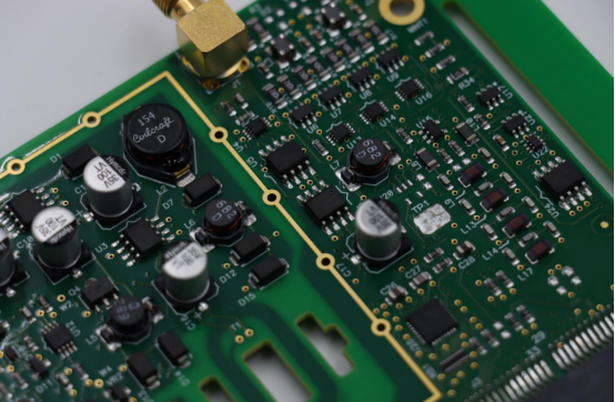
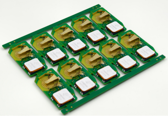
A printed circuit board (PCB) is the fundamental platform that allows electronic components to communicate with each other. It acts as both a mechanical support and an electrical connection system for components such as resistors, capacitors, and microchips. Instead of relying on loose wires, PCBs use copper traces—thin conductive pathways—etched or printed onto an insulating substrate to create precise electrical circuits.
In simple terms, a PCB is the skeleton and nervous system of an electronic device. It provides the structure that holds components in place while ensuring controlled and reliable electrical flow between them. This combination of structure and connectivity is what makes modern electronic design compact, efficient, and scalable.
There are three main types of PCBs, classified by the number of conductive layers:
Single-layer PCBs: Have one layer of copper; commonly used in simple devices like calculators or LED lights.
Double-layer PCBs: Contain two conductive layers, allowing more complex routing for consumer electronics such as audio systems.
Multilayer PCBs: Consist of three or more layers laminated together; essential for advanced applications like smartphones, servers, and medical equipment.
Each type serves a different balance between cost, complexity, and performance, reflecting the diversity of needs in electronic manufacturing.
Why Understanding PCB History Matters
The history of printed circuit boards tells the story of how electronics evolved from bulky, hand-wired assemblies to today’s miniaturized, high-speed systems. Every major step in PCB development—whether it was the introduction of copper-clad laminates, the invention of through-hole plating, or the shift to surface-mount technology—has directly influenced how we design and build electronic products.
For engineers and designers, understanding PCB history helps reveal why certain design standards exist and how manufacturing processes have adapted over time. For manufacturers, it offers insights into the origins of production methods that shape today’s efficiency, reliability, and sustainability. And for students or technology enthusiasts, the evolution of PCBs provides a clear window into how human ingenuity has driven progress in electronics.
From early point-to-point wiring to complex multilayer HDI boards, the journey of PCB innovation mirrors the rapid growth of modern technology. Appreciating this history not only connects us to the past—it also helps us imagine the next breakthroughs that will define the future of electronic design.
The Early Era of Electrical Wiring (Before PCBs)
Point-to-Point Wiring Systems
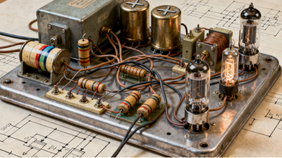
Before printed circuit boards were invented, electronic circuits were built using point-to-point wiring. In this method, engineers and technicians manually connected each component—such as resistors, capacitors, and vacuum tubes—by soldering wires directly between their terminals. Every connection had to be made by hand, often guided by simple schematic diagrams or visual layout boards.
This approach dominated the 1920s and 1930s, especially in devices like radio receivers, amplifiers, and early vacuum tube equipment. The components were usually mounted on metal chassis or insulating boards, and the wires ran freely between connection points. Some manufacturers tried to organize wiring using terminal strips or lug boards, but the result still looked like a tangled web of connections.
Point-to-point wiring worked well for simple circuits, but as designs grew more complex, it became increasingly difficult to manage. Every additional wire introduced a new chance for error—short circuits, loose connections, or signal interference—making consistency and mass production almost impossible.
In short, point-to-point wiring was functional but fragile, a labor-intensive technique that limited how small, reliable, and affordable electronics could become.
Limitations of Early Wiring
While point-to-point wiring marked an important step in early electronics, it had several major limitations that modern PCBs eventually solved.
1. Complexity and Human Error
As circuits became more sophisticated, the number of wires increased dramatically. Each manual connection raised the risk of mistakes during assembly or repair, making the process both tedious and error-prone. Troubleshooting faults in these dense wiring systems demanded extensive time and skill, as technicians had to trace individual connections through a maze of tangled wires to identify and correct issues.
2. Reliability Issues
Solder joints could weaken from heat or vibration, leading to intermittent failures that were difficult to detect. Crossed or uninsulated wires sometimes caused short circuits, posing both functional and safety risks. Moreover, inconsistent wiring layouts made it challenging to ensure uniform performance across devices, as variations in assembly could easily affect reliability and electrical characteristics.
3. Limited Scalability and Efficiency
Because every circuit had to be wired by hand, large-scale production was slow and expensive. Manufacturers struggled to maintain consistent quality across batches, as slight variations in assembly could impact performance. Additionally, devices built in this manner were bulky and heavy, leaving little room for miniaturization and limiting the design possibilities for more compact electronics.
Compared to these early methods, printed circuit boards (PCBs) introduced revolutionary advantages: compact size, consistent performance, automated production, and simplified repair. The transition from manual wiring to PCBs marked the beginning of true electronic manufacturing efficiency—a turning point that paved the way for modern technology.
The Birth of the Printed Circuit Concept (1900s–1940s)
Albert Hanson’s Early Patent (1903)
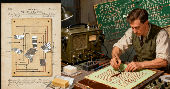
The idea of printing electrical circuits dates back to Albert Hanson’s 1903 patent, one of the earliest formal concepts of a printed circuit. Hanson envisioned conductive patterns applied to an insulating board as a way to replace messy, manual wiring. His design aimed to create organized electrical pathways that could carry current without the need for numerous loose wires.
Hanson experimented with materials such as foil, wax, and layers of dielectric substances to form these conductive paths. Although his methods were rudimentary and not yet widely adopted, they laid the conceptual groundwork for future developments. Essentially, Hanson introduced the principle of predefined conductive layouts on a stable base, which is the core idea behind modern printed circuit boards.
Charles Ducas and the “Printed Wiring” Innovation
In the 1920s, Charles Ducas advanced Hanson’s ideas by developing a method to stencil conductive ink directly onto boards. This technique allowed electrical connections to be “printed” rather than manually wired, significantly reducing the complexity of assembling circuits.
This innovation led to the creation of “printed wiring boards”, a term that reflects the method of depositing conductive patterns onto a substrate. Ducas’s approach was an early form of mass-producible circuit design, enabling more consistent layouts and the possibility of scaling up production. It represented a clear shift from hand-wired circuits toward standardized, repeatable electronic assemblies.
Technological Advancements and Mass Production
The early 20th century saw rapid advancement in printed circuit concepts, driven by the growing demand for miniaturized, reliable, and easily manufactured electronic circuits. These developments were especially important for communication and radio equipment, where consistent performance and compact design were essential.
Engineers began adopting early PCB-like assemblies to standardize components and layouts, enabling faster production, reduced assembly errors, and improved reliability in challenging environments. This period also encouraged experimentation with new materials, better insulation, and more efficient manufacturing techniques.
In essence, this era transformed printed circuit concepts from experimental ideas into practical, production-ready technologies, paving the way for the commercialization and widespread adoption of PCBs that would later revolutionize the electronics industry.
The Industrialization of PCBs (1950s–1970s)
The Rise of Copper-Clad Boards and Etching Techniques
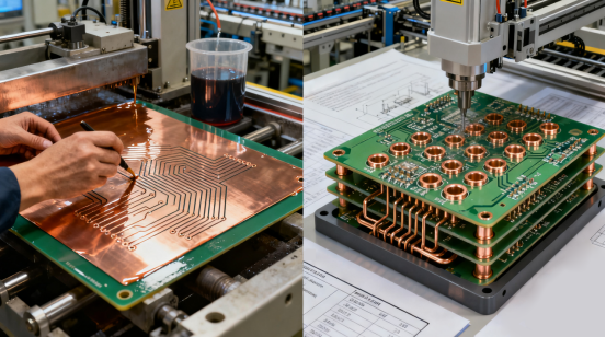
In the mid-20th century, the electronics industry transitioned from using printed conductive inks to copper-clad boards, which provided superior conductivity, durability, and precision. In this method, a thin layer of copper is bonded to an insulating substrate, creating the foundation for forming circuit patterns through chemical etching.
The production of copper-clad PCBs typically followed a step-by-step process:
1. Lamination – A copper foil is laminated onto a rigid insulating board, such as fiber-reinforced epoxy.
2. Photoresist Application – A light-sensitive coating is applied to the copper surface to define the circuit pattern.
3. Etching – The board is exposed to chemicals that remove unwanted copper, leaving only the desired conductive traces.
4. Drilling – Holes are drilled for component leads and interlayer connections.
This method produced more precise and reliable circuits than earlier printing methods and laid the groundwork for high-volume manufacturing of electronic assemblies.
Invention of Through-Hole Technology
During the 1950s and 1960s, through-hole technology emerged as a key innovation. This method involves plated through-holes, which are holes drilled through the PCB and coated with conductive material to electrically connect multiple layers.
Through-hole technology enabled multi-layer PCBs, allowing circuits to be stacked and connected in ways that were previously impossible. Early computers, industrial control systems, and consumer electronics all benefited from this advancement. For example, multi-layer PCBs made compact memory boards and complex control modules feasible, accelerating the development of more sophisticated electronic devices.
Standardization and Commercial Adoption
The mid-20th century marked the rise of standards and automation in PCB manufacturing. Organizations such as IPC introduced guidelines for board design, materials, and testing, helping the industry achieve greater consistency, quality, and interoperability.
Automated assembly lines further reduced production costs and improved reliability compared to hand-wired or early manual PCBs. Manufacturers could now produce large quantities of boards with fewer defects, making electronics more affordable and accessible.
In comparison, early PCBs and hand-wired systems were expensive, time-consuming, and prone to failure. By the 1970s, industrialized PCBs had become the backbone of consumer electronics, computers, and communication devices, marking a major milestone in the evolution of modern electronics.
The Digital Revolution and the Rise of Multilayer PCBs (1980s–2000s)
Surface Mount Technology (SMT) Emergence
In the 1980s, surface mount technology (SMT) emerged as a revolutionary method for assembling electronic circuits. Unlike through-hole assembly, where component leads pass through drilled holes in the PCB, SMT involves mounting components directly onto the board’s surface.
SMT brought several significant advantages:
Miniaturization: Components became smaller, allowing more circuits to fit on a single board.
Faster manufacturing: Automated pick-and-place machines could quickly position and solder components.
Higher circuit density: Boards could support complex designs with multiple connections without increasing size.
This technology became the standard for high-volume consumer electronics, transforming how devices were designed, manufactured, and repaired.
Evolution of Materials and Design Tools
During this period, PCB materials also advanced. Early laminates such as FR-1 and FR-2 were suitable for simple circuits but had limitations in heat resistance and mechanical strength. The introduction of FR-4, a fiberglass-reinforced epoxy laminate, provided greater durability, thermal stability, and reliability for high-speed digital circuits.
At the same time, computer-aided design (CAD) software revolutionized PCB layout. Engineers could now design complex multilayer boards with precise trace routing, component placement, and automated error checking. CAD tools enabled faster prototyping, reduced design errors, and streamlined communication between designers and manufacturers.
The Role of PCBs in the Personal Computer Boom
The rise of personal computers in the 1980s and 1990s accelerated PCB innovation. Companies like IBM, Apple, and Compaq demanded boards that could support increasingly powerful processors, memory modules, and peripheral interfaces.
A typical motherboard of the era illustrates the step-by-step role of PCBs in a computer:
1. Processor and chipset mounting – Central processing units were soldered onto the PCB using SMT.
2. Memory modules – RAM chips were connected through surface-mount or edge connectors.
3. Peripheral interfaces – Expansion slots, input/output ports, and controllers were integrated to allow communication with printers, monitors, and storage devices.
Without multilayer PCBs, these compact, high-performance systems would have been impossible. By enabling dense, reliable, and cost-effective electronic interconnections, multilayer boards helped drive the personal computer revolution, shaping the way people work, communicate, and consume technology.
Modern PCB Technology and Advanced Manufacturing (2010s–Present)
High-Density Interconnect (HDI) and Microvia PCBs
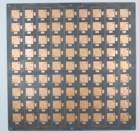
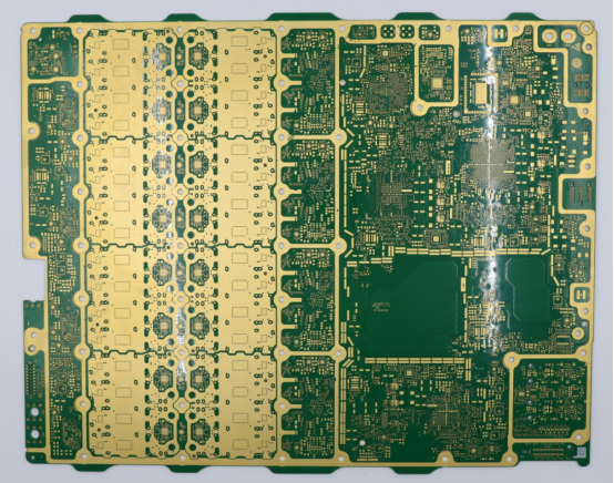
High-Density Interconnect (HDI) PCBs are advanced circuit boards designed to accommodate highly complex, compact electronic devices. They use microvias, which are extremely small holes that connect different layers of the PCB. This allows designers to fit more circuits into a smaller area without increasing the board size.
HDI PCBs are essential for modern devices that demand miniaturization and high performance, such as smartphones, wearables, and Internet of Things (IoT) boards. By enabling tighter component placement and shorter signal paths, HDI boards improve electrical performance, reliability, and device efficiency compared to traditional multilayer PCBs.
Rigid-Flex and Flexible PCBs
Flexible PCBs are circuits built on flexible substrates, allowing the board to bend or fold without breaking electrical connections. When combined with rigid sections, they are called rigid-flex PCBs, which provide both stability and flexibility in a single design.
The advantages of flexible circuits include:
Space-saving designs for devices where compactness is critical.
Durability under mechanical stress, reducing the risk of broken traces.
Simplified assembly by reducing the number of connectors between separate boards.
Common applications include medical devices, where boards must conform to small or curved spaces, and foldable electronics, like foldable smartphones or wearable tech, where traditional rigid boards cannot meet design constraints.
Environmental and Sustainability Trends
Modern PCB manufacturing increasingly focuses on environmental responsibility. Key practices include:
Lead-free soldering, which eliminates toxic lead in circuit assembly.
RoHS (Restriction of Hazardous Substances) compliance, ensuring PCBs meet strict chemical standards.
Recycling methods, which recover valuable metals like copper and gold from old boards.
In addition, researchers are developing bio-based PCB materials, such as substrates made from renewable fibers or biodegradable polymers. These innovations aim to reduce electronic waste and carbon footprint while maintaining performance standards for modern electronics.
By integrating advanced materials, miniaturization techniques, and sustainability practices, today’s PCB technology enables the creation of smaller, faster, and environmentally responsible devices, keeping pace with the demands of the digital era.
Future Directions and Emerging Innovations
3D Printed Electronics
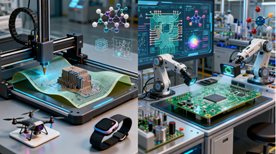
3D printed electronics use additive manufacturing techniques to build circuits layer by layer with conductive inks and polymers. Unlike traditional PCB fabrication, this method allows for the creation of custom geometries and complex 3D structures that were previously impossible with flat, multilayer boards.
The technology is particularly valuable for rapid prototyping, enabling engineers to test and iterate designs quickly without waiting for traditional PCB production cycles. For example, prototypes for sensors, wearable devices, or drone components can be printed and tested in a matter of hours, greatly accelerating the innovation process.
3D printed electronics also open new possibilities for integrated devices, such as embedding circuits directly into structural components or creating flexible and curved circuit paths for advanced applications.
Integration with AI and Smart Manufacturing
Artificial intelligence is increasingly shaping PCB design and manufacturing. AI-driven design optimization can analyze circuit layouts to reduce signal interference, minimize material use, and enhance thermal performance. Additionally, AI-powered defect detection identifies potential errors during production, improving yield and reducing costly rework.
The influence of Industry 4.0 is evident in smart factories where connected machines, real-time monitoring, and automated quality checks streamline PCB fabrication. AI integration not only enhances efficiency but also supports predictive maintenance and adaptive production, allowing manufacturers to respond quickly to changing product demands.
Predictions for the Next Decade
Looking ahead, PCB technology is expected to evolve in several transformative ways:
Nano-materials will enable smaller, faster, and more efficient circuits with improved electrical and thermal properties.
Optical interconnects may supplement or replace traditional copper traces, increasing data transfer speeds and reducing signal loss.
Sustainable production practices will expand, including bio-based substrates, greener etching chemicals, and fully recyclable PCBs.
These trends suggest that future electronics will be smaller, faster, more reliable, and environmentally responsible, driven by innovations that combine advanced materials, AI optimization, and additive manufacturing techniques.
Conclusion
Printed circuit boards have come a long way—from the manual point-to-point wiring of the early 20th century to today’s highly automated, multilayer, and flexible PCB systems. Each technological leap, from Hanson’s early conductive patterns to modern HDI and 3D printed electronics, has enabled smaller, faster, and more reliable electronic devices, powering the digital world we rely on every day.
PCB Development Timeline
Period | Key Milestone | Example / Innovation |
|---|---|---|
1903 | Albert Hanson’s early patent | Conductive patterns on insulating boards |
1920s | Charles Ducas “printed wiring” | Stenciled conductive ink, early mass-producible boards |
1940s | Technological advancements | Standardized circuits |
1950s–1970s | Industrialization of PCBs | Copper-clad boards, through-hole technology, IPC standards |
1980s–2000s | Digital revolution | SMT, multilayer boards, CAD design, personal computers |
2010s–Present | Advanced manufacturing | HDI, rigid-flex/flexible PCBs, sustainable materials |
Future | Emerging innovations | 3D printed electronics, AI-driven optimization, nano-materials, optical interconnects |
PCBs remain at the heart of modern electronics, shaping everything from smartphones and computers to medical devices and IoT systems. Understanding their history not only highlights past innovations but also provides insight into the future of electronics, including AI-optimized designs, nano-materials, and sustainable manufacturing practices.
If you have questions or want to learn more about PCBs, feel free to contact PCBMASTER. As a seasoned PCB supplier, we offer expert guidance and professional solutions for all your PCB needs.
FAQs
1. What was the first printed circuit board ever made?
The first printed circuit board concept was patented by Albert Hanson in 1903. He designed conductive patterns on an insulating board to replace manual wiring, laying the foundation for modern PCBs.
2. What is the difference between through-hole and surface-mount technology?
Through-Hole Technology: Component leads pass through drilled holes in the PCB and are soldered on the opposite side; provides mechanical strength.
Surface-Mount Technology (SMT): Components are mounted directly on the board’s surface without drilled holes; allows smaller, denser circuits, faster automated assembly, and higher reliability.
3. Who invented the printed circuit board?
The first formal PCB concept is credited to Albert Hanson (1903). Later, Charles Ducas (1920s) improved the method by stenciling conductive ink, creating early mass-producible “printed wiring boards.”
4. How are modern PCBs different from those made in the 1970s?
Modern PCBs feature:
Multilayer HDI and microvia designs versus mostly single- or double-layer boards in the 1970s.
Surface-mount technology (SMT) replacing through-hole assembly.
Advanced materials like FR-4 for improved thermal and electrical performance.
CAD and AI-assisted design, enabling faster, more reliable, and compact production.
Environmental compliance (RoHS, lead-free solder) and increased recyclability.


