


Star Grounding in PCB Design: Effective Noise Reduction for Better Signal Integrity
In the world of circuit design, one of the most crucial—and often overlooked—elements is how to manage ground connections. With the increasing complexity of mixed-signal systems, where analog and digital components coexist, achieving a clean, noise-free ground plane becomes essential. That's where star grounding comes into play. This approach helps isolate sensitive analog signals from the digital noise that could easily corrupt them, ensuring that your circuit runs smoothly and reliably. But while its benefits are clear, implementing star grounding comes with its own set of challenges. In this article, we’ll explore how star grounding works, its strengths and weaknesses, and when and why it’s the best choice for your designs.
Introduction to Star Grounding
Definition of Star Grounding
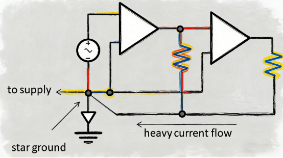
Star grounding is a method of connecting all the ground paths of a circuit to a single, central point. This central point is typically a low-impedance area, often a copper pad or copper pour, designed to reduce the electrical resistance between the ground connections. The goal is to provide a common reference point for all the components in a circuit, ensuring that the ground voltage remains stable and free from noise.
In simpler terms, imagine a star with its center at the middle and its points extending outward. Similarly, in star grounding, all ground wires (or traces) connect to a single center point, ensuring that each component's ground is at the same potential. This method is especially important in electronic circuits where noise can easily spread through ground connections, causing performance issues in sensitive components.
Why Star Grounding Matters
The significance of star grounding lies in its ability to isolate sensitive circuits and prevent interference from other parts of the system. In modern electronics, circuits often mix both analog and digital components. Analog circuits, like sensors or audio equipment, are sensitive to small fluctuations in voltage, while digital circuits, such as microcontrollers or processors, tend to generate electrical noise during switching. Without proper grounding, this digital noise can bleed into the analog circuits, causing errors or degraded performance.
By using star grounding, each type of ground—analog, digital, and power—is isolated and routed directly to the central "star" point. This separation minimizes the risk of noise affecting sensitive analog signals, creating a cleaner environment for signal transmission. In this way, star grounding ensures that digital and analog parts of the circuit do not interfere with each other, allowing for better overall performance.
For example, consider a medical device that measures body temperature using a sensor. The sensor's analog signal can be easily corrupted by noise from nearby digital circuits, such as the processor that controls the device. Star grounding ensures that the sensor's ground is isolated from the processor’s ground, reducing the chance of noise affecting the sensor’s accuracy.
In short, star grounding is critical for achieving clean signal transmission in systems with mixed analog and digital components, helping ensure that noise from one part of the circuit doesn’t degrade the performance of another.
How Star Grounding Works
Isolation Between Different Circuit Grounds
Star grounding works by isolating the ground paths for different parts of the circuit—typically the analog ground, digital ground, and power ground—and connecting them all to a single central point. Think of it like having separate highways for cars, trucks, and buses, all of which eventually meet at a common intersection. By isolating these grounds from each other, the interference that one part of the circuit might cause doesn’t affect the other parts.
For example, analog circuits, like those found in sensors, are very sensitive to small changes in voltage. Any noise from the digital circuits, which can be noisy due to switching signals from microcontrollers or processors, could cause problems. By separating the grounds, we ensure that the noise from the digital circuits doesn’t leak into the sensitive analog circuits.
Each group of circuits (analog, digital, and power) is connected to the central star point via its own dedicated trace. This prevents the different types of signals from interfering with each other, leading to more stable and accurate performance. The central point where all the grounds meet should have low impedance, ensuring a stable reference point for all circuits.
Prevention of Signal Interference in Mixed-Signal Circuits
In mixed-signal circuits, where both analog and digital components coexist, star grounding plays a key role in preventing signal interference. Digital circuits, like microcontrollers, create noise every time they switch between states (on/off). If this noise is allowed to travel through the ground, it can disturb analog signals.
For instance, imagine a sensor measuring heart rate. The sensor generates an analog signal that is very precise, but if the digital processor controlling the display of the heart rate is too close, it can emit noise that interferes with the sensor's signal. Star grounding solves this by isolating the ground paths of the digital processor from those of the sensor, so that the noise generated by the processor doesn't affect the sensor's output.
By creating dedicated, separate ground paths that meet only at a single point, star grounding ensures that the digital noise doesn’t contaminate the analog signal. This makes the system more reliable and accurate, especially in applications like medical devices, audio equipment, or sensor networks where precise data is crucial.
Key Considerations in Implementation
Selecting the Star Center
The star center is the key to making star grounding work effectively. It is where all ground traces converge. Choosing the right location and size for the star center is critical. A large copper pad or copper pour is typically used to create the star center. The reason for this is simple: a larger copper area offers lower impedance, meaning the signal can flow more easily and there will be less resistance at the connection point. This ensures the ground remains stable and doesn’t interfere with the other components in the circuit.
In practical terms, using a small star center could create unwanted resistance, making the ground less effective at isolating the different circuit grounds. The larger the copper pad, the better it can handle the electrical current, ensuring that the ground stays clean and noise-free.
Route Traces Appropriately
When implementing star grounding, one of the most important factors is the width of the traces used to connect the different grounds to the central star point. The analog ground traces, in particular, should be wide—typically at least 1mm—to lower impedance and reduce the chance of noise. Narrow traces can create high resistance, leading to higher impedance, which could allow noise to seep into the ground.
Wider traces also reduce the inductance (the resistance to changes in current) of the ground path, which is especially important for maintaining clean signals in low-frequency designs. For high-frequency circuits, minimizing impedance and ensuring short, wide traces is critical to maintaining signal integrity. In short, properly routing wide traces for analog grounds ensures a stable and low-noise environment for your sensitive circuits.
Practical Example of Implementation:
Let’s consider a small medical device that measures skin temperature using a thermistor. This device combines analog sensors with a microcontroller for digital processing. If star grounding is used, the ground path for the sensor (analog ground) is connected to the star center using a wide trace, ensuring minimal impedance. The microcontroller (digital ground) is isolated through separate traces. By doing this, the switching noise from the microcontroller does not leak into the sensor’s ground, allowing for accurate temperature measurements.
This demonstrates how the thoughtful implementation of star grounding with a large star center and wide traces ensures better signal integrity, which is crucial for precision in mixed-signal applications.

Pros and Cons of Star Grounding
Advantages
Optimized for Mixed-Signal Designs
Star grounding is particularly well-suited for mixed-signal designs, where both analog and digital components coexist. In these types of circuits, analog components (like sensors or audio equipment) need clean and stable signals to function properly. Digital components (like microcontrollers) often produce noise when they switch on and off, which can interfere with the analog signals.
By using star grounding, the digital and analog grounds are separated, ensuring that the noise from digital circuits does not leak into the analog signals. This is especially useful in IoT (Internet of Things) devices and portable medical devices, where you often have both analog sensors and a digital processor working together. Star grounding ensures each type of signal remains clean, improving the overall performance and reliability of the device.
For example, in a portable heart rate monitor, the sensor generating the analog signal must be isolated from the processor generating digital signals. Star grounding helps keep the heart rate measurement accurate by preventing digital noise from corrupting the analog sensor's signal.
Enhanced Debugging Capability
One of the main benefits of star grounding is its clear separation of ground paths. Since all the grounds are routed separately to the central star point, it becomes much easier to troubleshoot and debug the circuit. If there is an issue with one section of the circuit, such as a noisy signal or incorrect behavior, it's easy to identify which part of the grounding system is causing the problem.
In contrast, when all the grounds are combined into a single ground plane, noise can spread throughout the system, making it harder to isolate the problem. With star grounding, you can quickly pinpoint whether the issue is with the analog, digital, or power ground and take appropriate action. This simplifies the design process, especially for beginners or engineers working on small-scale projects.
For instance, if a temperature sensor in a medical device is giving erratic readings, the designer can check whether the digital circuit is leaking noise into the analog ground, thanks to the clear separation provided by star grounding.
Cost-Effective for Small Designs
For small printed circuit boards (PCBs), star grounding is a cost-effective option because it doesn't require the creation of a ground plane. A ground plane is a large area of copper that acts as a common ground for all components. While ground planes are essential in larger designs, they add to the cost and complexity of the PCB.
In contrast, star grounding uses a single copper pad or pour at the center, making it a more affordable option for small, simple designs. This can be particularly advantageous for prototypes, low-budget devices, or small consumer electronics that don’t require the complexity of a full ground plane.
For example, a simple IoT device like a temperature logger can benefit from star grounding, as it reduces the need for a costly ground plane while still providing clean signal paths.
Disadvantages
Scalability Issues
While star grounding is great for small circuits, it can become problematic when scaling up to larger PCBs. As the size of the board increases, the length of the ground traces also increases. This leads to higher inductance, which means the resistance to current flow increases, reducing the efficiency of the grounding system.
In large designs, the long traces required to connect all components to the star center can cause problems, including signal delays and potential interference. This makes star grounding less ideal for large, complex circuits where performance and efficiency are critical.
For example, in a large industrial control system, where hundreds of components are interconnected, the use of star grounding could lead to poor performance due to high inductance in the long ground traces.
Performance Limitations at High Frequencies
Star grounding has performance limitations at high frequencies, especially frequencies above 10 MHz. As the length of the ground traces increases, they can cause signal reflections. These reflections occur when signals bounce back from a long trace instead of flowing smoothly, causing distortion and potential data loss.
At high frequencies, it becomes difficult to maintain the clean and stable ground needed for accurate signal transmission. For high-speed applications, such as high-frequency communications or data processing, star grounding may not provide the necessary performance.
For example, in a high-speed communication system like Wi-Fi or 5G, where signals need to maintain integrity at very high frequencies, star grounding could cause problems, making a full ground plane more suitable.
Risk of Ground Loops
A ground loop is a situation where there are multiple ground paths, and the differences in voltage between these paths can cause unwanted currents to flow. This can result in hum, noise, or signal distortion in the system. In star grounding, ground loops can occur if the traces are not routed properly or if the connections to the star center are not directly made.
For example, if multiple components share a common ground but are connected to the star center at slightly different points, they may create a loop, causing noise or malfunctioning in sensitive analog circuits like audio systems or medical sensors.
To avoid ground loops, it’s essential to ensure that all ground traces are directly routed to the central star point without any detours or additional connections. This requires careful planning during the PCB layout process.
Best Use Cases for Star Grounding
Small Mixed-Signal Circuits (≤1 MHz Frequency)
Star grounding is particularly effective in small mixed-signal circuits, where both analog and digital components coexist, and the frequency range is relatively low (less than 1 MHz). In these types of circuits, precise grounding is critical because any noise or interference between the analog and digital components can cause errors in signal processing. Star grounding helps by isolating the digital circuits from the sensitive analog components, ensuring that the noise generated by digital devices does not interfere with the analog signals.
A typical example is a portable medical monitor that measures a patient's heart rate or blood oxygen levels. The analog sensors in the device generate precise signals that need to be accurately processed by the digital microcontroller. If the ground for both the analog and digital circuits were shared without separation, noise from the microcontroller could distort the sensor readings. By using star grounding, each ground path is separated, ensuring that the sensor readings remain accurate, even when the device is in use.
Another example of a small mixed-signal circuit is a sensor module that combines an analog sensor (like a temperature sensor) with a digital processor. Star grounding ensures that the analog signal from the sensor is not corrupted by noise from the digital processor, providing clear and reliable data.
Ideal Applications
IoT Devices with Analog Inputs
The Internet of Things (IoT) is a rapidly growing field, with devices such as smart sensors, wearable health monitors, and environmental monitoring systems that combine both analog and digital circuits. Star grounding is an ideal solution for these types of devices because it allows for the clean separation of grounds, preventing digital noise from interfering with analog sensors.
For example, a smart thermostat uses analog sensors to measure temperature and a digital processor to control the heating or cooling system. The sensor’s analog signal can be easily corrupted by noise from the digital circuits, causing inaccurate readings. By using star grounding, the ground for the sensor and the microcontroller are kept separate, ensuring that the sensor’s readings remain accurate.
This approach is also beneficial in smart agriculture, where IoT devices measure soil moisture, temperature, and other environmental factors using analog sensors, but need a digital controller to process the data. Star grounding ensures that the analog data is not disturbed by digital noise, making the system more reliable.
Low-Power Circuits
Star grounding is also highly effective in low-power circuits, where minimizing power consumption and cost is crucial. In these applications, the simplicity of star grounding—without requiring a full ground plane—helps keep the circuit design compact and affordable.
An example of a low-power circuit is a battery-operated sensor node used in remote environmental monitoring. These devices often rely on a mix of digital and analog components, like temperature sensors (analog) and a microcontroller (digital). Since the device is powered by a battery, power consumption must be minimized. Star grounding helps by ensuring that the ground paths are clean and noise-free, without the added complexity and cost of a ground plane.
Another example is a wireless sensor used in a smart home system. These sensors typically measure things like motion or humidity and need to transmit data to a central hub. Star grounding helps ensure the data from the sensor is accurate by preventing noise from the digital communication circuits from affecting the analog sensor signals. The simplicity and low cost of star grounding make it perfect for these small, low-power devices.
Practical Implementation of Star Grounding
Step-by-Step Guide to Star Grounding Setup
Setting up star grounding correctly is essential for minimizing noise and ensuring your circuit works reliably. Here’s a simple step-by-step guide to implement star grounding effectively:
1. Design Ground Planes and Layers
When designing the PCB, it's important to first decide how the grounds will be laid out. In star grounding, you’ll design separate ground planes for analog, digital, and power circuits. These planes or layers will each connect to the central star point, ensuring that each circuit is isolated from others.
You don’t need a ground plane for the entire board like in some designs, but dedicated layers for each ground type will help keep the paths clear and minimize interference. Keep in mind that for small designs, star grounding often doesn’t require a full ground plane, which makes it a cost-effective solution.
2. Choose Ground Traces Wisely
The next step is to choose the right width for the ground traces. The width of the traces plays a crucial role in ensuring low impedance, which helps prevent noise from leaking into the system. For analog circuits, the traces should be wider (at least 1mm) to reduce resistance and ensure the ground connection is stable.
For digital circuits, the traces don’t need to be as wide, but they should still be able to handle the current that flows through them. Make sure you consider the current flow and the circuit’s requirements when deciding how wide the traces should be.
In practical terms, wider traces create a better connection to the star point, and they reduce the risk of interference or voltage fluctuations, which can disrupt the signal.
3. Route Power, Analog, and Digital Grounds Separately
One of the key advantages of star grounding is that it isolates different types of grounds from each other. Route power, analog, and digital grounds separately to their respective areas. Each type of ground should have its own trace leading to the central star point.
For example, the digital ground will be connected from the microcontroller to the star point, while the analog ground will be routed from the sensor to the star center. This ensures that noise from the digital circuit doesn’t affect the sensitive analog signals.
Important Tip: Make sure that these grounds don’t share paths, as this could result in ground loops or noise interference.
4. Ensure Low-Impedance Connections to the Star Point
The star center is where all the ground paths converge, and it’s important to ensure that the connection to this point is low-impedance. A large copper pad or copper pour is often used as the star center to keep the impedance low and provide a stable reference point for all the ground connections.
In simpler terms, think of the star center as the “hub” where all the paths meet. To prevent noise and ensure stable operation, this point must have low resistance so that current can flow easily without disruption. If the star center is too small or the connection too weak, it could cause performance issues, especially if there are high currents flowing through the ground.
Troubleshooting Star Grounding in Circuits
Even with the best planning, issues can still arise. Here’s how to handle common problems in star grounding setups:
Common Issues: Improper Trace Routing, Ground Loops, and Impedance Mismatches
1. Improper Trace Routing: If ground traces aren’t routed correctly, they may interfere with each other or create high-inductance paths that degrade performance. Traces that are too long or poorly routed can lead to unwanted noise.
2. Ground Loops: Ground loops occur when there are multiple paths for the current to return to the star center. This can cause voltage differences between different parts of the ground, leading to unwanted noise or signal distortion.
3. Impedance Mismatches: If the ground traces are too narrow or not designed properly, they can create impedance mismatches that affect signal integrity, especially in analog circuits.
Solutions: Shorter Trace Lengths, Better Trace Widths, and Proper Isolation Techniques
1. Shorter Trace Lengths: Keep the ground traces as short as possible. Longer traces introduce higher inductance, which can cause signal delays and reduce performance. Routing traces in a compact way minimizes this issue.
2. Better Trace Widths: Ensure the analog ground traces are wide enough (≥1mm) to handle the required current without introducing too much resistance. This helps prevent impedance mismatches and ensures a clean ground path.
3. Proper Isolation: If you suspect ground loops or noise interference, check that each ground trace is isolated and goes directly to the star center. Use separate traces for analog and digital grounds, ensuring that they do not share paths at any point. This isolation keeps the analog signals clean and free from digital noise.
For example, if you have a temperature sensor that is giving unstable readings, the issue might be that the digital ground is interfering with the analog ground. In this case, make sure both are routed separately and check that all traces are short and wide enough to minimize impedance.
Star Grounding vs. Ground Plane: Key Differences
Star Grounding
Star grounding is a technique commonly used in small designs, especially when dealing with low-frequency applications (typically below 1 MHz). It involves connecting all ground paths to a single central point, creating a "star" shape. Each type of ground (analog, digital, power) is routed separately to this central point, minimizing the chance of digital noise affecting sensitive analog signals.
Best for Small Designs and Simpler Setups
Star grounding works best in small PCBs where the design is simple and doesn't require complex grounding solutions. This makes it ideal for applications such as IoT devices, sensor modules, or portable medical monitors, where the circuit size is compact, and the frequency range is low.
For example, in a small medical thermometer, star grounding helps isolate the sensor's analog signals from the microcontroller's digital signals, ensuring accurate readings. Because the circuit is simple and operates at low frequencies, star grounding is enough to maintain signal integrity without the need for more complex solutions like ground planes.
Best for Low-Frequency Applications
Star grounding is also particularly effective in low-frequency applications (below 1 MHz) where signal integrity is crucial, but the frequency isn’t high enough to require the complex features of a ground plane. Since low-frequency signals are less sensitive to the issues caused by long ground traces, star grounding can provide a clean and stable ground without the need for extensive layouts.
For instance, a simple analog temperature sensor circuit could benefit from star grounding, where the analog signal doesn’t need to be protected from high-frequency noise, and the ground path is straightforward.
Ground Plane
In contrast, a ground plane is a large, continuous sheet of copper used as the ground for all components on a PCB. This technique is highly effective in reducing electromagnetic interference (EMI) and providing stable current return paths for high-frequency signals. It is best suited for large circuits and high-frequency applications (typically above 10 MHz), where signal quality and power integrity are critical.
Best for Large, High-Frequency Circuits
Ground planes are essential in large PCBs or designs that need to manage high-frequency signals, such as high-speed digital circuits or radio-frequency (RF) systems. In these cases, a continuous ground plane provides a direct and low-resistance path for the return currents, ensuring that the signal integrity is maintained even at high frequencies.
For example, in a high-speed communication system, a ground plane helps to minimize signal reflections and noise. The large area of copper helps to return currents from the signal traces quickly and without creating unnecessary loops, making it an excellent choice for circuits that need to handle high-speed data transmission or operate in RF environments.
Better Noise Reduction and Current Return Paths
Ground planes offer superior noise reduction compared to star grounding because of their continuous nature. The solid copper layer covers the entire board, offering a uniform path for the return currents. This is particularly important in high-frequency designs, where electromagnetic interference can significantly impact signal quality. The ground plane helps shield sensitive circuits from external noise and ensures that the currents flowing through different parts of the circuit return to the ground without causing interference.
For instance, in radio transmitters, the ground plane reduces the risk of unwanted interference by providing a stable, continuous return path for currents, preventing them from traveling through unintended routes and causing noise or signal degradation.
Star Grounding vs. Ground Plane: Comparison Table
Feature Star Grounding Ground Plane Best for Small designs, simple setups, low-frequency applications Large designs, high-frequency circuits Ground Layout Central star point with separate traces for each ground Continuous copper layer covering the entire PCB Noise Reduction Minimizes digital noise in small, low-frequency circuits Superior noise reduction for high-speed and RF circuits Current Return Path Separate traces for each ground type, meeting at the star point Continuous, uniform return path across the entire board Scalability Not ideal for large PCBs due to long ground traces Ideal for large PCBs with complex and high-speed circuits Complexity Simple, easy to implement for small projects More complex, requires careful layout for high-frequency designs Common Applications IoT devices, portable medical monitors, small sensor modules High-speed digital circuits, RF systems, large communication systems
Common Mistakes in Star Grounding
Star grounding is a powerful technique for minimizing noise and ensuring clear signal paths in your circuit. However, there are common mistakes that can undermine its effectiveness. Let’s explore the key issues you should avoid to ensure proper implementation of star grounding.
1. Improper Trace Length and Width
One of the most common mistakes in star grounding is using long, narrow traces for the ground connections. These traces can introduce inductance—a form of resistance that slows down the current flow and makes it harder for the circuit to function properly. Inductance can cause signal delays and reduce the overall performance of the system.
Why it matters: In star grounding, you want the ground paths to be as short and wide as possible. Long traces create more resistance and higher inductance, which can lead to noisy signals and performance issues. Narrow traces increase resistance, which affects the current flow and can cause voltage drops.
Real-life example: Imagine a temperature sensor circuit where the analog signal is sensitive to small voltage changes. If the ground trace leading to the star center is too long or narrow, it could introduce noise that distorts the sensor reading, leading to inaccurate data.
Solution: Keep the ground traces as short as possible. For analog grounds, make the traces wider (at least 1mm) to reduce resistance and ensure smooth current flow. For digital grounds, use appropriately sized traces, but remember that long, narrow traces should be avoided.
2. Overloading the Star Center
Another common mistake is overloading the star center by connecting too many ground paths to the single point where all the grounds converge. This can cause noise and signal degradation, which defeats the purpose of star grounding.
Why it matters: The star center acts as the common reference point for all ground connections. If you route too many traces to this point, the central connection can become a bottleneck. This can cause higher impedance at the central point, which could allow unwanted currents or noise to flow through the ground, affecting the performance of the entire circuit.
Real-life example: Suppose you’re designing a small medical monitoring device with several sensors and a microcontroller. If too many grounds (analog, digital, power) are connected to the star center at once, you could introduce noise into the ground system. This could lead to inaccurate readings or even system instability, especially in sensitive components like the sensor.
Solution: Limit the number of connections at the star center. If necessary, use multiple star centers for different groups of circuits (such as one for analog grounds and one for digital grounds) to avoid overloading the main star point. This ensures that the ground paths remain clean and noise-free.
3. Ignoring Ground Loops
A critical mistake in star grounding is ignoring ground loops. Ground loops occur when there are multiple paths for the ground current to return to the star center, but they are not routed properly. This can create voltage differences between different parts of the ground system, resulting in unwanted interference and signal distortion.
Why it matters: When ground loops occur, the circuit becomes prone to noise, which can affect sensitive components, particularly in mixed-signal circuits where both analog and digital components are present. If the ground paths are not properly routed or if they share connections, noise can travel through the circuit, causing instability.
Real-life example: Consider a sensor module that combines an analog sensor with a microcontroller. If there is a ground loop between the analog sensor’s ground and the digital processor’s ground, the noise from the digital processor can affect the sensor’s output, leading to inaccurate readings.
Solution: Ensure that all ground paths lead directly to the star center without any detours or shared paths. Each component should have its own dedicated trace leading to the star center, keeping the analog and digital grounds isolated. This isolation helps prevent ground loops and ensures that the system operates smoothly.
Conclusion
Star grounding is a simple, cost-effective solution for noise isolation, making it ideal for small, mixed-signal circuits like IoT devices, medical monitors, and sensor applications. By isolating ground paths to a single central point, it prevents interference between analog and digital components, ensuring clean signal transmission. This method is perfect for low-frequency, small-scale projects where performance and cost efficiency are crucial.
However, for larger or high-speed designs, star grounding can face limitations due to long traces and inductance. In such cases, ground planes or hybrid approaches offer better performance, providing a continuous path for current return and improved signal integrity.
If you're working on small, low-frequency projects, star grounding is a reliable choice. For larger, more complex systems, consider using ground planes to achieve the best results. For any further questions or professional guidance on PCB design, don’t hesitate to reach out to PCBMASTER, your trusted PCB supplier, for expert advice.
FAQs
What is the primary benefit of using star grounding in PCB design?
The primary benefit of star grounding in PCB design is its ability to isolate different circuit grounds, which minimizes the risk of noise interference between components. By connecting all grounds to a single central point (the "star center"), star grounding ensures that analog, digital, and power grounds do not interact or affect each other. This isolation helps maintain clean signal paths, especially in mixed-signal designs, where noise from digital circuits can disrupt analog signals. In simple terms, it creates clear, dedicated paths for each type of ground, reducing the chances of signal corruption and improving overall circuit performance.
Can star grounding be used in high-frequency designs?
Star grounding is not ideal for high-frequency designs (those above 10 MHz). While it works well for low-frequency applications (≤1 MHz), it starts to lose effectiveness at higher frequencies due to long trace lengths. In high-frequency circuits, long traces introduce inductance, which can cause signal reflections and disrupt the performance of the circuit. These reflections can lead to signal integrity problems, especially in high-speed data transmission or RF applications. Therefore, while star grounding is great for low-frequency or small circuits, for high-frequency designs, it is generally better to use ground planes, which provide continuous, low-inductance paths for current return, ensuring stable signal performance.
How do I ensure proper isolation in mixed-signal designs using star grounding?
To ensure proper isolation in mixed-signal designs (designs with both analog and digital components) using star grounding, follow these key steps:
1. Separate the ground traces: Use distinct ground paths for analog, digital, and power components. Each type of circuit should have its own dedicated trace leading to the star center.
2. Wide traces for analog grounds: Since analog signals are sensitive to noise, make the ground traces for analog circuits wider (at least 1mm). This reduces impedance and minimizes any potential noise interference.
3. Short and direct routing: Keep the traces as short as possible and ensure that each ground path leads directly to the star center. Avoid detours or shared paths, which could cause unwanted ground loops.
4. Use multiple star centers if necessary: If the design is complex, consider using multiple star centers—one for analog circuits and another for digital circuits—to ensure complete isolation.
By following these practices, you can achieve the necessary signal isolation in mixed-signal designs, minimizing the impact of digital noise on analog signals.
What are the common pitfalls of star grounding?
Several common pitfalls can undermine the effectiveness of star grounding and degrade the overall performance of your circuit:
1. Long trace lengths: If the ground traces are too long, they can introduce inductance, which affects the current return path and increases the likelihood of signal reflections. This is especially problematic in high-frequency circuits.
2. Improper trace routing: If the traces are not routed correctly or efficiently, they may cause interference between ground paths or contribute to ground loops. Avoid making unnecessary loops or detours in the ground traces.
3. Ground loops: These occur when multiple paths exist for the return current to the star center, and the traces are not properly isolated. This can lead to unwanted voltage differences across the ground, causing interference or signal distortion.
4. Overloading the star center: Too many ground paths connected to the central star point can create a high-impedance connection, which compromises the noise isolation benefits of star grounding. Keep the star center as simple as possible, ideally with separate points for analog and digital grounds if necessary.
Being mindful of these common mistakes and addressing them during the design phase can help you maintain the integrity of your circuit and achieve better performance.
Is star grounding suitable for large-scale PCB designs?
Star grounding is generally not suitable for large-scale PCB designs due to its inherent limitations in scalability. The main issues include:
1. Long trace lengths: In larger circuits, the traces connecting to the star center become longer, which increases inductance and can lead to signal degradation and improper current return paths. This is particularly problematic in high-speed or high-frequency designs.
2. Impedance mismatch: As the design size increases, the impedance of the traces may vary, causing signal reflections and other issues that affect the circuit’s overall performance.
3. Overloading the star center: In large designs, there may be multiple grounds that need to be connected to the star center. Overloading this central point can lead to noise issues and grounding problems.
For large or complex designs, it is often better to use a ground plane, which provides a continuous, low-impedance path for current return and ensures stable signal integrity. A ground plane can be easily scaled to accommodate larger circuits, whereas star grounding tends to struggle with larger designs due to the increased length of traces and the complexity of isolating grounds effectively.
If your project involves high-speed or large-scale PCBs, a ground plane or hybrid grounding method (combining both star grounding and ground planes) may be the best option for optimal performance.
Author Bio
Hi, I'm Carol, the Overseas Marketing Manager at PCBMASTER, where I focus on expanding international markets and researching PCB and PCBA solutions. Since 2020, I've been deeply involved in helping our company collaborate with global clients, addressing their technical and production needs in the PCB and PCBA sectors. Over these years, I've gained extensive experience and developed a deeper understanding of industry trends, challenges, and technological innovations.
Outside of work, I'm passionate about writing and enjoy sharing industry insights, market developments, and practical tips through my blog. I hope my posts can help you better understand the PCB and PCBA industries and maybe even offer some valuable takeaways. Of course, if you have any thoughts or questions, feel free to leave a comment below—I'd love to hear from you and discuss further!

