


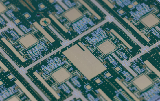
Ground Planes: The Gold Standard in PCB Design
Grounding is a critical factor in PCB design, influencing everything from signal integrity to electromagnetic compatibility. Among the various techniques, ground planes have earned their reputation as the gold standard. These continuous copper layers not only provide a reliable return path for currents but also serve as shields against interference, ensuring that the signals remain clean and stable. With their ability to enhance performance across a range of applications, from consumer electronics to high-speed communications, ground planes are essential in achieving optimal results in modern PCB designs.
Introduction to Ground Planes
Brief Introduction to the Importance of Grounding in PCB Design
In PCB (Printed Circuit Board) design, grounding is essential for ensuring that electrical signals flow smoothly without interference. A proper grounding system prevents electrical noise, reduces the risk of signal distortion, and ensures that the circuit performs reliably. Without grounding, circuits may malfunction due to unstable voltages, leading to poor performance or even damage. Proper grounding is particularly crucial in high-frequency applications, where even small disturbances can have significant effects on the overall system.
Definition of Ground Planes and Why They Are Considered the "Gold Standard"
A ground plane is a continuous layer of copper on a PCB used to provide a stable ground reference for the circuit. It serves as a return path for electrical currents and acts as a shield against electromagnetic interference (EMI). Ground planes are often referred to as the "gold standard" in PCB design because they offer superior performance compared to other grounding methods. Unlike traditional ground traces, which can introduce noise or resistance, a ground plane minimizes impedance and ensures more efficient current flow. This results in improved signal integrity, reduced noise, and better overall performance in the finished product.
Ground planes are especially valued in high-speed, high-frequency designs where even minor grounding issues can result in significant performance degradation. Their ability to effectively manage return currents and shield sensitive components makes them the go-to solution for most modern PCBs.
Overview of How Ground Planes Impact the Performance of Modern PCBs
Ground planes have a significant impact on the performance of modern PCBs in several ways:
1. Improved Signal Integrity: By providing a low-impedance path for return currents, ground planes help maintain clean signals with minimal distortion. This is particularly important in circuits handling high-speed signals, where signal integrity is critical for accurate data transmission.
2. Reduction in Electromagnetic Interference (EMI): Ground planes act as a shield, blocking unwanted external electromagnetic signals that could interfere with the PCB's functionality. This shielding reduces noise and ensures that sensitive components are protected from external sources of interference.
3. Minimizing Ground Loops: A ground plane helps prevent ground loops, which occur when there are multiple ground paths with different potentials. Ground loops can cause unwanted currents that disrupt the operation of the circuit, leading to noise or erratic behavior. Ground planes provide a uniform grounding environment, minimizing the risk of ground loops.
4. Simplified Layout: Ground planes simplify the PCB layout by reducing the need for complex ground trace routing. This not only saves time during design but also improves the overall reliability and manufacturability of the board.
In practice, these benefits make ground planes indispensable in devices such as smartphones, laptops, industrial control systems, medical equipment, and other high-frequency devices. Their ability to manage currents, shield against noise, and ensure a stable ground connection makes them essential for achieving optimal performance in a wide range of applications.
Project Example: How a Ground Plane Affects Signal Integrity in a High-Speed PCB Design
Imagine you're designing a PCB for a high-speed data transfer system, such as a 5G antenna. Without a ground plane, the return currents of the signal traces might not flow directly beneath the signal traces. This can create a larger loop area, which introduces noise and distorts the signal. Additionally, external EMI could interfere with the data transmission, leading to errors or slow performance.
By incorporating a ground plane beneath the signal traces, you ensure that the return currents flow directly beneath the signal, minimizing the loop area and reducing noise. Furthermore, the ground plane shields the circuit from external EMI, ensuring clean, stable data transmission. This makes the PCB more reliable and effective, highlighting the importance of ground planes in high-performance designs.
How Ground Planes Improve PCB Performance
Ground planes improve PCB performance by providing a low-impedance path for return currents, reducing signal distortion and noise. They also shield the circuit from electromagnetic interference (EMI), protecting sensitive signals. Additionally, ground planes eliminate ground loops, ensuring more stable and reliable signal integrity, which is crucial for high-speed and precision applications.
Low-Impedance Path for Return Currents
A ground plane is a solid, continuous layer of copper in a PCB that acts as a path for return currents. When a signal travels along a trace, it needs a return path to complete the circuit. Without a ground plane, this return path can become longer or less direct, increasing impedance (resistance to the flow of current) and causing signal distortion.
With a ground plane, the return currents flow directly beneath the signal traces, creating a low-impedance path. This reduces resistance and ensures that the signal travels more efficiently, maintaining its integrity. In high-speed circuits, where precise signals are critical, this low-impedance path helps reduce signal loss and minimize noise.
Real-life example: In high-speed data transmission circuits, such as those in smartphones or 5G systems, using a ground plane ensures that the signals can travel at their intended speed without interference. This results in clearer communication and faster data speeds.
EMI Shielding and Protection
One of the most important functions of a ground plane is EMI shielding. Electromagnetic interference is unwanted noise that can distort or completely disrupt the normal operation of a circuit. This interference can come from various sources, like nearby electrical devices or radio frequencies.
A ground plane works as a protective barrier by absorbing and blocking external electromagnetic fields. It essentially acts like a Faraday cage, which is a conductive enclosure that prevents electromagnetic signals from entering or leaving a designated area. By covering the PCB with a continuous copper ground plane, it shields the sensitive components from external noise, ensuring that the signal remains clean and reliable.
Real-life example: Medical devices like MRI machines are highly sensitive to EMI because they need to operate in environments with minimal interference. By using ground planes, these devices maintain high accuracy in their readings and prevent the data from being corrupted by external electrical noise.
Minimizing Ground Loops and Signal Interference
A ground loop occurs when multiple ground connections in a circuit have different voltages, creating unwanted currents that can interfere with the system. These loops can introduce noise and cause instability, especially in audio or sensor systems.
A ground plane eliminates this problem by providing a single, unified ground reference across the entire PCB. Since the ground plane is continuous, all components share the same ground potential, preventing the creation of ground loops. As a result, the entire system is less likely to experience signal interference or voltage fluctuations.
Additionally, ground planes reduce electromagnetic interference (EMI) by acting as a shield that absorbs or redirects unwanted signals. This shielding can reduce EMI by as much as 20 dB—a significant improvement for reducing noise in high-precision systems.
Real-life example: In industrial control systems, where precise measurements are critical, using ground planes prevents the distortion of signals from sensors or actuators. This ensures that the system operates accurately, reducing the risk of malfunction or error.
Design Considerations for Implementing Ground Planes
Layer Stack-up for Multi-Layer PCBs
When designing multi-layer PCBs, the layer stack-up plays a critical role in ensuring the ground plane performs optimally. Typically, the ground plane is placed on Layer 2, with the power plane on Layer 3. This configuration helps isolate the signal layers (such as the top and bottom layers) from noise and interference.
Placing the ground plane adjacent to the signal layers ensures that the return currents flow directly beneath the signal traces, minimizing the loop area and reducing impedance. This arrangement provides excellent shielding, keeping the signals clean and reducing electromagnetic interference (EMI). Proper layer stack-up also helps with signal isolation, ensuring that high-speed signals don’t interfere with sensitive components or other signal traces.
Real-life example: In a 4-layer PCB for a smartphone, Layer 1 is used for high-speed signal traces (e.g., USB or HDMI), Layer 2 is the ground plane, Layer 3 is the power plane, and Layer 4 handles other signal traces. This design reduces noise between components and ensures stable performance across the device.
Via Stitching and Inter-layer Grounding
Via stitching involves placing vias (small conductive holes) to connect ground planes across multiple PCB layers. This ensures that the ground plane is continuous and provides a stable return path for currents. Without proper via stitching, the ground plane may have gaps or interruptions, leading to increased impedance and potential noise.
The spacing of vias is important. Ideally, vias should be placed 5–10mm apart to ensure efficient current flow and maintain a low-impedance connection between layers. Insufficient spacing can cause high-frequency signals to become unstable, leading to signal integrity issues.
Real-life example: In high-speed PCBs, such as those used in 5G antennas, via stitching is essential to keep the ground planes connected across layers. If vias are too far apart or incorrectly placed, the device might experience signal loss or degradation, impacting overall performance.
Placement and Routing Challenges
One common placement issue in PCB design is the creation of dead spots—areas where the ground plane is disconnected or interrupted. This can happen if traces or other components block the ground plane, causing noise and instability in the circuit. Dead spots can result in signal distortion and increased EMI.
To avoid dead spots, it’s important to route ground traces carefully to ensure that the ground plane remains intact and continuous. This includes placing components and vias strategically so that the ground plane is not disrupted. Additionally, use wide ground traces or areas of copper to maintain low impedance and reduce resistance.
Best practices for routing include:
Avoiding narrow or long traces that can increase resistance.
Maintaining copper pours for larger ground connections.
Ensuring sufficient via stitching for better inter-layer grounding.
Real-life example: In a high-performance graphics card, ensuring continuous ground paths and proper via stitching is critical. Any dead spots or interruptions in the ground plane could lead to visual artifacts or instability during high-frame-rate processing, which is undesirable for gaming or professional applications.
Advantages and Disadvantages of Using Ground Planes
Advantages
Effective Across All Frequencies, from DC to 100 GHz
A ground plane is highly effective across a broad range of frequencies, from direct current (DC) signals to high-frequency signals reaching up to 100 GHz. This versatility makes ground planes ideal for various applications, whether they are low-speed circuits (like power supplies) or high-speed systems (like radio frequency (RF) or wireless communication circuits).
At high frequencies, maintaining proper grounding becomes critical to minimize noise, signal degradation, and interference. Ground planes help by providing a low-impedance return path for current, reducing the chances of signal distortion and ensuring the integrity of high-speed signals.
Real-life example: In 5G antennas and high-speed digital circuits, using ground planes ensures that the signals can be transmitted with minimal interference and signal loss, allowing for faster and more reliable data transfers.
Simplified Routing and Design Processes
One of the biggest advantages of using a ground plane is the simplified routing of PCB traces. Instead of manually routing individual ground connections, the ground plane offers a ready-made, low-resistance path for current to flow back to the power supply. This significantly reduces the complexity of the PCB layout, saving both time and effort during the design process.
The continuous copper ground plane eliminates the need for multiple separate ground traces, making the design process cleaner and more straightforward. This is especially useful in high-density PCBs, where space is limited, and routing can otherwise become complicated.
Real-life example: In the design of smartphones, the use of ground planes allows engineers to route complex circuits efficiently without worrying about additional ground traces. This results in a compact, functional, and reliable design.
Improved System Reliability Due to Reduced Noise and EMI
Ground planes also enhance system reliability by reducing electromagnetic interference (EMI) and noise. The continuous copper layer helps shield the circuit from external electromagnetic fields, preventing them from disrupting the sensitive signals on the PCB. By maintaining a solid ground connection, ground planes minimize the chances of ground loops, which can cause unwanted noise and errors in signal processing.
In systems where precise signal processing is crucial, such as medical equipment or industrial control systems, using a ground plane can significantly improve performance by reducing potential sources of interference.
Real-life example: In medical imaging systems like MRIs, ground planes are used to prevent external EMI from affecting the quality of the images. This ensures that the data collected is clear and reliable, which is vital for accurate diagnoses.
Disadvantages
Increased Cost Due to Additional PCB Layers
One of the main drawbacks of using ground planes is the increased cost. Since ground planes require additional layers in the PCB, this results in a higher manufacturing cost. For multi-layer PCBs, the process of adding extra layers, such as the ground and power planes, increases material usage and production time.
Although the cost increase is generally minor for most designs, it can be significant for very large or high-volume products. This can be a factor to consider, especially when designing low-cost consumer electronics.
Real-life example: In consumer electronics like budget smartphones, designers may opt for fewer layers to reduce costs. While ground planes are important, some simpler devices may prioritize cost-efficiency over the added benefits of ground planes.
Potential Layout Complexity, Requiring Careful Planning
Another disadvantage of ground planes is the layout complexity they introduce. While the ground plane simplifies routing in some ways, it also requires careful planning to avoid problems such as dead spots or gaps in the plane. If traces, vias, or components are placed incorrectly, it could disrupt the continuity of the ground plane, leading to issues like increased noise or signal interference.
The placement of components must be carefully considered to ensure that the ground plane remains intact and uninterrupted. Designing an efficient multi-layer PCB with a ground plane requires a clear understanding of the electrical properties and how they affect signal integrity.
Real-life example: In high-speed digital circuits for servers, engineers need to plan the layout carefully to ensure that the ground plane doesn’t have gaps, which could result in signal degradation. This makes the layout process more time-consuming and technically demanding.
Heavier Than Trace-Based Grounding (Though Negligible for Most Designs)
Ground planes are generally heavier than trace-based grounding, since they cover larger areas of the PCB. While this weight is often negligible for most designs, it can be a factor in specialized applications such as aerospace or wearable electronics, where weight is a critical concern.
In such cases, trace-based grounding (using narrow copper traces for grounding) might be preferred to minimize the overall weight of the PCB. However, for most consumer electronics and industrial applications, the added weight of ground planes does not significantly impact the design or performance.
Real-life example: In aerospace electronics, weight is a critical consideration, and engineers might choose a more lightweight grounding approach. However, for smartphones, the added weight of a ground plane is not a concern compared to the benefits it provides in terms of performance and noise reduction.
Common Ground Plane Design Mistakes to Avoid
Incorrect Layer Stack-up
The layer stack-up in a multi-layer PCB determines how the ground and power planes are positioned relative to signal layers. If ground planes or power planes are placed in the wrong layers, it can lead to various problems. For example, placing the ground plane too far away from the signal layers can increase impedance, resulting in signal degradation or increased noise.
A common mistake is to place the power plane directly next to the signal layer without a ground plane nearby. This can cause ground bounce and voltage fluctuations, affecting the stability of high-speed signals.
Best Practice: Ground planes should be placed close to signal layers, ideally on adjacent layers (e.g., Layer 2 as ground and Layer 3 as power) to improve signal integrity and minimize EMI.
Real-life Example: In a 4-layer PCB used for a high-speed communication system, Layer 1 might be used for signal traces, Layer 2 as the ground plane, Layer 3 as the power plane, and Layer 4 for additional signal traces. If the ground plane is too far away from the signal traces, the system might experience signal degradation or interference, especially in high-frequency applications like Wi-Fi or 5G devices.
Inadequate Via Stitching
Via stitching refers to the use of vias (small conductive holes) to connect different ground planes across multiple layers of a PCB. Proper via stitching ensures that the ground planes remain electrically continuous, maintaining a low-impedance path for current to flow back to the power source.
If via density is too low or the vias are spaced too far apart (more than 10mm), the ground plane connection becomes weak, leading to voltage fluctuations, high impedance, and increased noise. This can impact high-speed signal transmission, causing signal integrity problems and electromagnetic interference (EMI).
Best Practice: To maintain efficient grounding, ensure that stitching vias are placed 5-10mm apart to ensure strong, stable connections across layers.
Real-life Example: In a PCB for a 5G antenna system, if the vias connecting the ground planes are too far apart, the system might experience signal instability or EMI, which could result in dropped signals or slower data transmission speeds. Proper via stitching helps maintain the high-speed performance of the system.
Inconsistent Ground Plane Connection
An inconsistent ground plane connection occurs when there are gaps or disruptions in the ground plane, often caused by improper routing of traces or placement of components. These disruptions create areas with high impedance, which leads to ground loops, noise, and signal distortion.
For a reliable and stable PCB design, the ground plane should remain continuous throughout the board. Any interruption in the ground plane can cause voltage fluctuations, disrupt return currents, and increase the chances of EMI.
Best Practice: Ensure that the ground plane is continuous and uninterrupted by routing traces, vias, or components in a way that maintains the integrity of the plane.
Real-life Example: In an industrial control PCB, where precision is crucial, any gaps in the ground plane could lead to sensor signal errors or malfunctioning actuators due to incorrect or unstable signals. Keeping the ground plane intact is vital for ensuring the correct functioning of the system.
Optimizing Ground Plane Design for Maximum Efficiency
Using Solid Ground Planes vs. Split Ground Planes
When designing PCBs, engineers often need to decide between using a solid ground plane or split ground planes. A solid ground plane is a single, continuous layer that spans the entire PCB. This design offers several benefits, including low impedance, better signal integrity, and reduced electromagnetic interference (EMI) because all return currents flow through the same continuous path. It's especially beneficial for high-speed circuits and systems that require strong EMI shielding.
However, in some cases, a split ground plane is used. This design divides the ground plane into separate regions, usually to reduce noise coupling between different areas of the PCB. For example, a split ground plane may be used to isolate sensitive analog circuits from noisy digital circuits. While this can improve performance in specific regions, it may also create grounding issues if not designed carefully. Gaps between these regions can lead to increased impedance and signal instability.
Real-life example: In an audio processing PCB, a split ground plane might be used to separate the analog audio section from the digital control section to avoid digital noise interference. However, if the separation isn’t managed well, it could lead to poor performance or even grounding issues.
Ground Plane Sizing and Coverage
Proper ground plane sizing is essential for achieving maximum performance and efficiency in a PCB design. The ground plane should be large enough to cover the entire area where signal traces are placed, providing a continuous path for return currents. Insufficient coverage can lead to increased impedance, causing signal degradation and making the PCB more susceptible to noise.
A general rule of thumb is to cover the entire PCB with a solid ground plane, ensuring it extends under all the signal traces. This reduces the risk of introducing high-impedance paths and ensures the signal’s return path is as direct as possible. Additionally, a larger ground plane helps to shield the entire PCB from external electromagnetic interference (EMI).
Real-life example: In high-speed PCB designs like those used for 5G technology, the ground plane must be sized appropriately to handle the fast return currents. If the ground plane is too small, the signal integrity can suffer, leading to performance issues or data transmission errors.
Minimizing Ground Plane Interruptions
Interruptions in the ground plane, such as cuts, gaps, or isolated sections, can severely affect the performance of a PCB. These interruptions increase impedance and can create noise or interference that disrupts the stability of the entire circuit. Proper design practices should be followed to minimize these issues and ensure the continuity of the ground plane.
Some common ground plane interruptions include:
Traces running through the ground plane: Signal traces or power traces running through the ground plane can disrupt its continuity and cause noise or signal loss.
Via holes or components in the ground plane: While vias are necessary for connecting different layers, placing too many vias or components in the ground plane can cause isolation and reduce the effectiveness of the grounding.
Cuts for thermal management or component placement: While these cuts may be needed for practical reasons, they should be minimized and strategically placed to avoid negatively impacting performance.
Best Practice: Use ground pours (large copper areas) instead of individual traces for grounding to ensure better continuity and fewer interruptions. If cuts are necessary, make sure they are minimized in size and placed in non-critical areas.
Real-life example: In a power supply PCB, interruptions in the ground plane could lead to increased noise levels, affecting the stability of the voltage regulation. Keeping the ground plane continuous helps maintain stable power delivery and reduces ripple or voltage spikes.
Ground Planes in Advanced PCB Technologies
High-Frequency Designs and Signal Integrity
In high-frequency PCB designs, such as those used in 5G technology, Wi-Fi systems, and high-speed digital circuits, the ground plane plays a critical role in ensuring signal integrity. At high frequencies, even small imperfections in the PCB layout can lead to signal degradation, noise, and crosstalk between different signals.
The ground plane provides a return path for the current, and if it is not carefully designed, it can increase the impedance of the return path, which leads to poor signal quality. For high-speed circuits, it is crucial that the ground plane be continuous, with no gaps or interruptions, to minimize electromagnetic interference (EMI) and signal reflection. Additionally, the distance between the ground plane and the signal traces should be kept as small as possible to reduce parasitic inductance and ensure the signals are transmitted accurately.
Best Practices for High-Frequency Designs:
Keep the ground plane as close as possible to the signal traces to ensure a low-impedance path for return currents.
Use solid ground planes instead of split planes to maintain a continuous return path.
Minimize via use and ensure that the vias used for connecting the ground planes are placed optimally to avoid additional inductance or resistance.
Real-life Example: In 5G PCB designs, the ground plane must be designed to minimize noise and interference. If the ground plane is not placed correctly, the high-frequency signals used for 5G communication can experience signal loss or distortion, resulting in poor data transfer speeds or dropped connections.
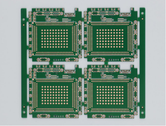
Multi-Layer and High-Density PCBs
As PCBs become multi-layered and high-density, designing the ground plane efficiently becomes a bigger challenge. Multi-layer PCBs typically include multiple signal layers, power layers, and ground planes. In such designs, ground planes must be carefully distributed across the layers to ensure that every signal has a direct and low-impedance return path. This is particularly important in high-density designs, where space is limited, and the signals are transmitted at high speeds.
One common challenge in multi-layer PCBs is ensuring proper grounding across all layers. A ground plane on one layer should be connected to the ground plane on other layers using via stitching. Insufficient via stitching or poorly placed vias can cause high-impedance paths, resulting in signal degradation or voltage fluctuations. Additionally, in high-density PCBs, it becomes crucial to manage the placement of components and vias to avoid disrupting the ground plane’s continuity.
Key Design Considerations:
Efficient use of via stitching: To ensure low-impedance connections between ground planes across layers, vias should be placed every 5–10mm.
Minimize trace length: Shorter traces for signals reduce resistance and prevent signal delay or reflection.
Ensure proper layer stack-up: In multi-layer PCBs, placing the ground plane next to signal layers (e.g., Layer 2 as ground, Layer 3 as power) minimizes noise and signal interference.
Real-life Example: In consumer electronics like smartphones, the PCB design involves multiple layers to accommodate the complex circuitry. A solid ground plane helps maintain high-speed data transfer, reduces EMI, and ensures the device operates efficiently. However, in high-density designs, managing the ground plane across multiple layers is essential to avoid performance issues such as signal loss or interference between power and signal traces.
Conclusion
Optimizing ground plane design is crucial for achieving high-performance, reliable PCBs, especially in high-frequency and multi-layer applications. A well-designed ground plane reduces noise, enhances signal integrity, and ensures the stability of your system. Whether you're designing a high-speed circuit or tackling a high-density multi-layer PCB, careful attention to ground plane layout is essential for success.
If you have any further questions or want to learn more about PCBs, feel free to reach out to PCBMASTER. As a seasoned PCB supplier, we provide expert guidance and solutions tailored to your specific needs. We're here to help you optimize your designs and achieve the best possible performance.
FAQs
Why is a ground plane important in PCB design?
A ground plane is crucial in PCB design because it provides a low-impedance return path for current, which reduces electromagnetic interference (EMI) and helps maintain signal integrity. By offering a continuous, stable path for return currents, a ground plane ensures reliable performance, especially in high-speed or sensitive circuits.
What is the difference between a ground plane and a ground trace?
A ground plane is a large, continuous copper layer used to reduce impedance and improve EMI shielding. It provides a much more effective grounding solution than a ground trace, which is a smaller, typically less efficient, path routed for grounding. Ground traces may suffer from higher impedance, leading to signal degradation or increased noise.
How does a ground plane help with electromagnetic interference (EMI)?
Ground planes act as a Faraday cage, blocking external electromagnetic interference (EMI) and preventing it from affecting the sensitive circuits on the PCB. The continuous copper layer absorbs stray electromagnetic fields, ensuring that signals remain clean and interference-free.
What is the optimal layer stack-up for a 4-layer PCB with a ground plane?
A typical 4-layer PCB stack-up with a ground plane is:
Top Layer (Signal)
Layer 2 (Ground Plane)
Layer 3 (Power Plane)
Bottom Layer (Signal)
This stack-up allows for efficient signal routing, improved EMI shielding, and optimal power distribution.
Can ground planes be used in flexible PCBs?
Yes, ground planes can be used in flexible PCBs, but the design requires special attention. Flexible PCBs are bendable or stretchable, so the layout must ensure that the ground plane maintains electrical continuity while accommodating the flexibility of the design. Proper placement of vias and routing is essential to maintain signal integrity in flexible applications.
Author Bio
Hi, I'm Carol, the Overseas Marketing Manager at PCBMASTER, where I focus on expanding international markets and researching PCB and PCBA solutions. Since 2020, I've been deeply involved in helping our company collaborate with global clients, addressing their technical and production needs in the PCB and PCBA sectors. Over these years, I've gained extensive experience and developed a deeper understanding of industry trends, challenges, and technological innovations.
Outside of work, I'm passionate about writing and enjoy sharing industry insights, market developments, and practical tips through my blog. I hope my posts can help you better understand the PCB and PCBA industries and maybe even offer some valuable takeaways. Of course, if you have any thoughts or questions, feel free to leave a comment below—I'd love to hear from you and discuss further!

