Hybrid Grounding Solutions for High-Frequency and Mixed-Signal PCBs
When it comes to high-speed, mixed-signal systems, traditional grounding methods simply can't keep up. From aerospace to 5G tech, the demand for crystal-clear signal integrity and minimal noise is pushing engineers to rethink how circuits are grounded. Enter hybrid grounding: a smart blend of techniques designed to tackle the unique challenges of today’s complex electronics. By seamlessly combining single-point and multi-point strategies, it ensures that both analog and digital signals stay pristine. Ready to see why this approach is revolutionizing modern circuit design? Let's take a closer look.
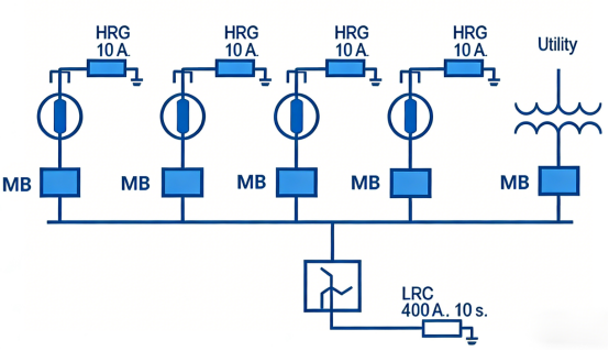
Overview of Hybrid Grounding in PCB Design
Definition of Hybrid Grounding in PCB Design
Hybrid grounding in PCB (Printed Circuit Board) design refers to the technique of combining different grounding methods—such as single-point and multi-point grounding—within a single circuit design. This approach is used to address the specific needs of complex systems, particularly those that involve both analog and digital signals. Unlike traditional designs that rely on one grounding method, hybrid grounding optimizes performance by using multiple strategies tailored to different parts of the system.
For example, in a mixed-signal PCB, low-frequency analog components might use single-point grounding, while high-frequency digital or RF (radio frequency) components rely on multi-point grounding through dedicated ground planes. This combination ensures that each part of the circuit performs efficiently without introducing unwanted interference or noise.
Importance of Hybrid Grounding in High-Frequency Mixed-Signal Systems
In high-frequency mixed-signal systems, such as those found in communication equipment or medical devices, the signals used can be very sensitive to noise and interference. Analog and digital components often have different grounding requirements. Analog signals, which are slower and more sensitive, need a stable, noise-free ground to maintain signal integrity. On the other hand, digital signals are faster and can generate high-frequency noise that can affect the performance of analog components if not properly isolated.
Hybrid grounding ensures that both types of signals can coexist on the same PCB without degrading each other’s performance. For example, a medical ultrasound system might have analog transducers that require clean grounding, while the digital processors need a different grounding setup to handle their high-speed operations. By using hybrid grounding, engineers can achieve a design where both analog and digital circuits operate without interference.
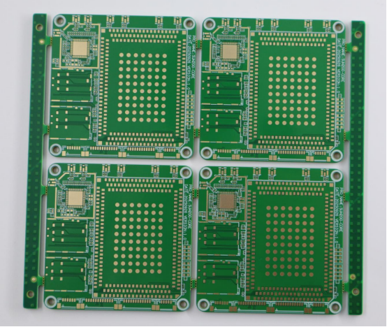
Understanding Grounding Methods in Electronics
Grounding is a fundamental aspect of electronic design that helps ensure circuits function properly and maintain signal integrity. In this section, we will explore two main grounding methods—single-point grounding and multi-point grounding—and the crucial role of ground planes in supporting these techniques. These methods are essential for managing noise, interference, and signal clarity in different types of circuits
Single-Point Grounding
Description of Single-Point/Star Grounding
Single-point grounding, also known as "star grounding," connects all components of a circuit to a single central ground point. This central point acts as the common reference for the entire system. In a star grounding configuration, all ground wires from various circuit parts converge at one location, forming a "star-like" pattern.
Applications in Low-Frequency (Analog) Circuits
Single-point grounding is commonly used in low-frequency analog circuits where noise and interference are more easily introduced. By ensuring that all components share the same ground reference, star grounding helps prevent voltage differences between ground points that can lead to unwanted noise or signal distortion. For example, in an analog audio system, where the quality of the sound is sensitive to noise, using single-point grounding ensures that the audio signal remains clean.
Benefits: Noise Prevention, Simplicity
The primary benefit of single-point grounding is its ability to prevent ground loops, which occur when there are multiple ground paths with slight differences in voltage. Ground loops can create unwanted hum or noise in audio, video, and other analog signals. Single-point grounding avoids this by using one central ground point. Additionally, it is simple to design and easy to implement, making it ideal for less complex circuits. It ensures that there is only one path for the ground current, reducing the chance of interference.
Multi-Point Grounding
Concept of Multi-Point Grounding (via Ground Planes)
Multi-point grounding involves connecting multiple ground points to a shared ground plane, distributing the ground connection across the system. Rather than relying on a single connection point, the ground is spread over a large area. This method is often used in high-frequency or digital circuits, where signal integrity is critical. In these systems, multiple points along the PCB are connected to a ground plane, which serves as a continuous, low-resistance path to ground.
Applications in High-Frequency (Digital/RF) Circuits
Multi-point grounding is commonly used in high-frequency digital circuits, such as radio-frequency (RF) systems or modern microprocessor designs. These circuits operate at high speeds, which can generate noise or cause "ground bounce" if not properly grounded. By using a ground plane, the ground reference is distributed evenly across the PCB, preventing noise from affecting sensitive digital signals. For instance, in a 5G base station, multi-point grounding ensures that high-speed digital signals can transmit without interference from noise or other signals.
Benefits: Reduced Ground Bounce, Signal Integrity
One of the key benefits of multi-point grounding is its ability to reduce ground bounce. Ground bounce occurs when different parts of a circuit experience slight variations in ground potential due to the high-speed switching of digital signals. Multi-point grounding ensures that the ground reference is stable, reducing the risk of ground bounce and improving signal integrity. By providing a low-resistance path to ground over the entire system, it ensures that digital signals remain clear and accurate, even at high speeds.
Ground Planes and Their Role
Definition and Function of Ground Planes in PCBs
A ground plane is a large area of copper on a PCB that serves as the main path for the system's ground connections. Ground planes are used in multi-point grounding to provide a continuous, low-resistance connection for all components. They act as a stable reference for the circuit's ground, helping to minimize noise and ensure that signals travel without interference. Ground planes are often placed on dedicated layers of the PCB, separate from signal traces, to keep the ground connection free from noise or unwanted currents.
How Ground Planes Support Multi-Point Grounding
In multi-point grounding, ground planes are crucial for connecting multiple components to a common ground without introducing additional resistance or noise. The ground plane provides a large, stable surface that all ground connections can tap into, ensuring uniformity across the circuit. For example, in high-frequency RF circuits, using a solid ground plane helps ensure that the ground reference is consistent, reducing noise that could interfere with sensitive signals. Ground planes also help with power distribution, as they allow the power supply to deliver voltage to components with minimal fluctuations.
Comparison Table: Single-Point vs. Multi-Point Grounding
Feature Single-Point Grounding Multi-Point Grounding Ground Reference One central ground point Distributed ground via ground plane Best for Low-frequency analog circuits High-frequency digital/RF circuits Noise Prevention Prevents ground loops, reduces noise in analog signals Reduces ground bounce and improves signal integrity Complexity Simple, easy to design More complex, requires careful PCB layout and design Signal Integrity Can be affected by noise in high-frequency designs Ensures stable signal integrity, especially at high speeds Use Case Example Audio systems, simple analog circuits RF communication systems, high-speed digital circuits
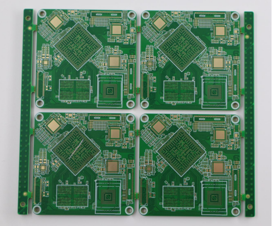
Hybrid Grounding Approach
Hybrid grounding combines different grounding techniques to address the specific needs of both analog and digital circuits. This approach optimizes signal integrity, reduces noise, and ensures high performance in complex systems. In this section, we’ll explore how combining single-point and multi-point grounding, along with tools like ferrite beads and optocouplers, helps create a stable and interference-free environment for both low- and high-frequency signals.
Combining Single-Point and Multi-Point Techniques
Rationale for Using Both Methods in High-Performance Designs
In high-performance systems, such as those in aerospace, telecommunications, and medical electronics, both analog and digital circuits must coexist without interfering with each other. Single-point grounding works well for analog circuits, where the risk of noise from multiple ground paths is high. However, multi-point grounding is essential for digital circuits to ensure that high-frequency signals are stable and clean. Combining both methods allows for optimal performance by addressing the specific needs of each circuit type. By selectively applying each grounding method based on the signal type, engineers can reduce noise and ensure high signal integrity.
Tailoring Grounding Strategies Based on Frequency Range
The key to hybrid grounding is customizing the grounding approach based on the frequency of the signals being used. Low-frequency signals (typically below 1 MHz) are more sensitive to noise and benefit from the simplicity of single-point grounding. On the other hand, high-frequency signals (above 10 MHz), which are more prone to interference and require stable ground references, benefit from multi-point grounding via ground planes. By tailoring the grounding technique for each frequency range, hybrid grounding helps optimize both analog and digital circuits in complex systems.
Practical Example: Combining Analog Sensors with Digital Processors in Aerospace Systems
In aerospace applications, such as satellite systems, hybrid grounding is particularly valuable. Analog sensors (e.g., temperature or pressure sensors) require single-point grounding to avoid interference from digital noise. At the same time, the digital processors that manage communication and data processing require multi-point grounding via dedicated ground planes to maintain the accuracy of high-speed signals. By using a hybrid grounding approach, the analog and digital components are isolated from each other, ensuring that both can function without interference, leading to reliable performance in critical systems like satellites.
The Dual-Frequency Grounding Strategy
Low-Frequency (<1 MHz) Circuits: Using Single-Point Grounding
Low-frequency circuits, typically operating below 1 MHz, are often used for analog signals that require stable, noise-free grounding. For these circuits, single-point grounding is the ideal choice. This technique ensures that the entire system shares a single, common ground reference, minimizing the risk of ground loops or voltage differences. This is especially important in applications like audio equipment, where even small amounts of noise can significantly degrade performance. By using a single ground point, these analog systems remain clean and free from interference.
High-Frequency (>10 MHz) Circuits: Using Multi-Point Grounding via Ground Planes
High-frequency circuits, particularly those operating above 10 MHz, require a different grounding approach to maintain signal integrity. These circuits, such as digital processors, RF systems, and communication systems, benefit from multi-point grounding. In this approach, a ground plane is used to provide a low-resistance path to ground across the entire PCB. This ensures that the high-speed signals are stable and reduces the chances of signal degradation or noise interference. Ground planes provide a continuous, stable ground reference, allowing high-frequency circuits to function optimally in environments where noise and interference are common.
Ferrite Beads and Optocouplers for Isolation
Role of Ferrite Beads in Blocking High-Frequency Noise
Ferrite beads are small components made of ferrite material that act as filters to block high-frequency noise. They are commonly used in hybrid grounding systems to prevent digital noise from interfering with sensitive analog signals. When placed in series with a signal line or ground path, ferrite beads effectively absorb and dissipate high-frequency noise, preventing it from traveling through the circuit. For example, in a medical device that uses both analog sensors and a digital processor, ferrite beads can be placed between the two domains to isolate noise from the digital circuits, ensuring the analog signals remain clear and accurate.
How Optocouplers Electrically Isolate Analog and Digital Domains
Optocouplers, also known as optical isolators, are electronic components that use light to transmit signals between two electrically isolated circuits. In a hybrid grounding design, optocouplers are often used to electrically isolate analog and digital domains, preventing noise from the digital side from affecting the analog signals. The optocoupler works by converting an electrical signal into light, which is transmitted through an optical medium and then converted back to an electrical signal on the other side. This isolation ensures that the analog and digital circuits can function independently, even when they share the same ground plane. For example, in a communication system, optocouplers are used to separate high-speed digital signals from analog signal paths to prevent noise and ensure data accuracy.
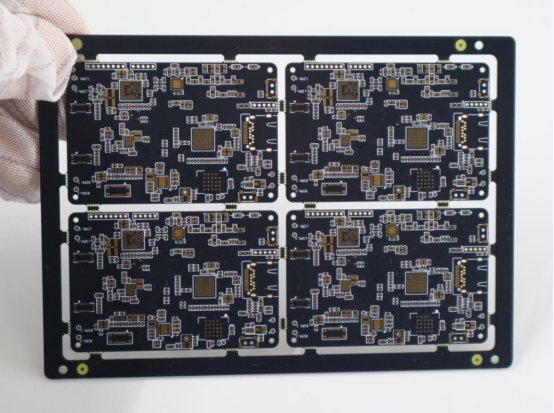
Implementing Hybrid Grounding in Complex Designs
In complex electronic systems, implementing hybrid grounding ensures both analog and digital circuits perform optimally while reducing interference. This section will focus on the essential design considerations for hybrid grounding, such as selecting grounding methods based on frequency and circuit complexity. It will also explore practical applications of hybrid grounding in systems like aerospace, 5G base stations, and medical devices.
Design Considerations for Hybrid Grounding
Key Parameters for Deciding Grounding Method (Frequency, Circuit Complexity)
When choosing a grounding method for a complex design, the primary factors to consider are frequency and circuit complexity. Low-frequency signals (below 1 MHz) are often best handled with single-point grounding, which reduces the risk of noise and ensures signal stability. High-frequency signals (above 10 MHz), however, require multi-point grounding with ground planes to maintain signal integrity and prevent interference. Additionally, the complexity of the circuit plays a significant role in the choice of grounding. For systems with many components and mixed signal types, hybrid grounding combines both methods to cater to each part of the circuit’s needs, ensuring reliability and performance.
Component Selection (e.g., Ferrite Beads, Capacitors)
Choosing the right components is crucial for effective hybrid grounding. Ferrite beads are commonly used to block high-frequency noise between analog and digital circuits. By placing these components in the ground path or signal lines, they absorb high-frequency interference, preventing it from crossing over into sensitive analog parts. Capacitors are also vital for filtering and stabilizing signals, especially in mixed-signal circuits where both analog and digital components are present. When designing a hybrid grounding system, careful selection of ferrite beads, capacitors, and other isolation components ensures the system remains noise-free and performs reliably under high-speed conditions.
Practical Applications in Complex Systems
Aerospace: Satellite PCBs with Analog and Digital Ground Separation
In aerospace, especially satellite systems, hybrid grounding ensures that analog and digital components remain isolated. Analog sensors like temperature and pressure sensors require single-point grounding to prevent interference from digital noise. Meanwhile, digital processors benefit from multi-point grounding via ground planes, ensuring stable operation at high frequencies. This approach ensures both analog and digital circuits function reliably in challenging environments like space.
5G Base Stations: Handling Mixed Analog and Digital Signals
5G base stations handle both analog and digital signals, each requiring different grounding methods. Analog components, like those for signal conditioning, use single-point grounding to preserve signal quality. In contrast, high-speed digital circuits use multi-point grounding with ground planes to prevent signal degradation from interference. Hybrid grounding ensures reliable data transmission and signal integrity across the system.
Medical Devices: Isolating Sensitive Analog Signals (e.g., Ultrasound Transducers) from Digital Processors
In medical devices such as ultrasound machines, hybrid grounding is crucial to maintain the accuracy of sensitive analog signals from ultrasound transducers. These analog signals, vital for diagnosis, require single-point grounding to avoid noise. Meanwhile, high-speed digital processors rely on multi-point grounding to prevent interference. This isolation ensures that the device operates precisely and reliably, delivering accurate medical results.
Challenges and Solutions in Hybrid Grounding
While hybrid grounding offers many advantages, it comes with its own set of challenges. These challenges often stem from the design complexity, component sourcing, and the need for simulation and verification to ensure that the grounding strategy works as intended. In this section, we’ll explore these challenges and discuss solutions to address them.
Design Complexity
Increased Design Time and Validation Process
Hybrid grounding requires careful planning and attention to detail, which can increase design time. Since both single-point and multi-point grounding need to be applied in different areas of the system, the design process becomes more intricate. Each circuit type, whether analog or digital, must be treated with its specific grounding requirements, which can lead to longer development cycles. Additionally, ensuring that the grounding methods don’t interfere with each other requires thorough testing and validation, further extending the design timeline.
Need for Advanced Simulation Tools (e.g., Ansys SIwave) to Verify Grounding Effectiveness
To effectively manage this complexity, designers often rely on simulation tools like Ansys SIwave to model and verify grounding effectiveness. These tools allow engineers to simulate the electrical behavior of the entire system, testing how well the grounding methods isolate noise and ensure stable signal integrity. By using these advanced simulation tools, designers can catch potential issues early in the design phase, reducing the likelihood of costly changes during physical testing.
Component Sourcing and Cost
Selecting and Sourcing Appropriate Isolation Components (e.g., Ferrite Beads, Optocouplers)
Hybrid grounding often requires additional components, such as ferrite beads and optocouplers, to ensure effective noise isolation. Ferrite beads block high-frequency noise, while optocouplers provide electrical isolation between sensitive analog and digital circuits. Sourcing these components can be challenging due to their specific requirements in hybrid grounding designs. Designers must select components that match the operational frequencies and isolation needs of their systems. This adds a layer of complexity to sourcing and procurement.
Balancing Cost Versus Design Benefits
Adding isolation components increases the cost of the overall design. While these components improve performance by reducing noise and ensuring signal integrity, they can also drive up the price of the final product. Therefore, designers must carefully balance the benefits of using these components against the added costs. In some cases, using higher-quality components like specialized ferrite beads or more expensive optocouplers may be necessary, but in other cases, cost-effective alternatives can still achieve the desired results.
Simulation and Verification
Importance of Simulation in Ensuring Noise Isolation
Since noise isolation is critical in hybrid grounding, simulation plays a key role in ensuring its effectiveness. Proper simulation helps identify potential interference issues before physical testing begins. By modeling the grounding system, engineers can predict how well the system will isolate noise between analog and digital components, preventing issues such as ground loops or signal degradation. Accurate simulations are crucial for confirming that the system meets both performance and electromagnetic compatibility (EMC) standards.
Key Tools and Techniques for Verifying Hybrid Grounding Performance
Several simulation tools and techniques are commonly used to verify hybrid grounding performance. In addition to Ansys SIwave, HyperLynx and Cadence are also popular tools for simulating signal integrity and grounding effectiveness. These tools allow engineers to test how the grounding system will behave under different conditions and verify that noise isolation is maintained. Techniques like time-domain reflectometry (TDR) and network analyzers can also be used in physical testing to verify that the actual system performs as expected.
Advantages of Hybrid Grounding
Hybrid grounding is a powerful technique used in modern electronics to address complex challenges, especially in systems that combine both analog and digital signals. This approach offers several key benefits, including noise reduction, signal integrity, compliance with EMC standards, and scalability for large systems. Let’s explore these advantages in more detail.
Noise Reduction and Signal Integrity
How Hybrid Grounding Minimizes Noise in Mixed-Signal Circuits
In mixed-signal circuits, where both analog and digital signals coexist, noise from one domain can easily interfere with the other. Hybrid grounding minimizes this risk by using single-point grounding for analog circuits and multi-point grounding for digital circuits. This separation helps ensure that noise from high-speed digital signals does not affect sensitive analog signals, maintaining their accuracy and clarity. By isolating these circuits with different grounding methods, hybrid grounding effectively reduces electromagnetic interference (EMI) and ground loops, common sources of noise in mixed-signal systems.
Benefits in Signal Clarity and Data Accuracy for High-Speed Systems
Hybrid grounding is particularly beneficial in high-speed systems, where maintaining signal integrity is critical. High-frequency digital signals are prone to degradation due to noise, and even small disturbances can lead to data errors. By isolating the analog and digital grounds, hybrid grounding ensures that signals remain clean, improving data accuracy and signal clarity. For example, in a 5G communication system, hybrid grounding allows for smooth data transmission by ensuring that high-speed signals are not corrupted by noise from analog components like signal conditioning circuits.
Compliance with EMC Standards
Meeting Industry Standards Such as CISPR 22 for Consumer Electronics
In today’s electronics, devices must meet strict electromagnetic compatibility (EMC) standards to prevent interference with other equipment. CISPR 22, a standard for consumer electronics, is one of the most widely used benchmarks for EMC compliance. Hybrid grounding plays a crucial role in meeting these standards by minimizing EMI, which can disrupt nearby devices. By ensuring that noise generated by digital circuits doesn’t interfere with analog components, hybrid grounding helps devices pass EMC testing, making them safer for consumer use.
Role of Hybrid Grounding in Reducing Electromagnetic Interference
Electromagnetic interference is a significant concern in sensitive electronic systems, especially those that handle mixed analog and digital signals. Hybrid grounding addresses this challenge by using ground planes to provide a stable ground reference for high-frequency signals. This reduces the risk of EMI, ensuring that systems like satellite communication equipment or medical devices do not interfere with other nearby electronics. By keeping the analog and digital circuits electrically isolated, hybrid grounding reduces the chances of electromagnetic radiation affecting system performance or violating regulatory standards.
Scalability for Large Systems
How Hybrid Grounding Supports Large, Multi-Domain PCB Designs
As electronic systems grow more complex, multi-domain PCBs require grounding solutions that can handle large, diverse components. Hybrid grounding offers scalability by enabling different grounding methods for various parts of the system. This flexibility allows engineers to design large-scale systems, such as server farms or complex communication networks, without compromising signal integrity. By applying hybrid grounding, engineers can ensure that each component—whether analog or digital—receives the appropriate grounding treatment for optimal performance.
Scalability in Complex Electronics Systems like Medical Equipment and Communication Infrastructure
In medical equipment and communication infrastructure, the need for scalable and reliable grounding is even more critical. Medical devices, such as ultrasound machines, rely on hybrid grounding to ensure that sensitive analog signals are free from noise while supporting complex digital processors. Similarly, in large-scale communication systems like 5G base stations, hybrid grounding allows for efficient signal transmission across various circuits, from RF components to high-speed processors. This scalability ensures that both simple and highly complex systems benefit from hybrid grounding, maintaining performance and reliability in a wide range of applications.
Limitations and Trade-offs
While hybrid grounding offers numerous advantages, it also comes with certain limitations and trade-offs that designers must carefully consider. These include design complexity, the need for rigorous testing and validation, and cost considerations for additional components and tools. In this section, we’ll explore these challenges and provide insights into how to navigate them.
Design Complexity and Validation
The Need for Rigorous Testing and Validation to Confirm Grounding Performance
Hybrid grounding introduces complexity into the design process, especially when combining multiple grounding methods for analog and digital circuits. Ensuring that both grounding techniques work together effectively requires thorough testing and validation. Engineers must perform a series of tests to verify that the system remains stable, and noise is properly isolated. This validation process can take time and resources, as it involves both simulation (using tools like Ansys SIwave) and physical testing to confirm that grounding methods do not interfere with each other. Any failure to validate correctly may lead to problems, such as ground loops or signal degradation, which could compromise the system’s performance.
Cost Considerations
Additional Costs of Components and Simulation Tools
One of the key trade-offs when implementing hybrid grounding is the cost. Hybrid systems often require specialized components, such as ferrite beads, optocouplers, and capacitors, to ensure proper isolation between analog and digital circuits. These components can add up, especially if high-quality parts are necessary to meet specific performance standards. Additionally, advanced simulation tools (e.g., Ansys SIwave, HyperLynx) are essential for verifying the grounding design, but they often come with significant licensing and maintenance fees. These costs can be a burden for smaller projects or budgets.
Weighing the Benefits Against the Increased Expenses
When considering hybrid grounding, designers must balance the benefits of improved signal integrity, reduced noise, and better compliance with standards against the increased expenses. While the improved performance and reliability justify the cost in many high-performance applications (such as medical devices or 5G networks), for simpler designs, the cost of components and simulation tools may not be worthwhile. It’s important to evaluate whether the added expense results in a measurable performance improvement, especially for systems that don’t require the highest levels of noise isolation or EMC compliance.
Conclusion
Hybrid grounding is a powerful solution to the complex challenges of high-frequency and mixed-signal PCB designs. By combining single-point and multi-point grounding techniques, it effectively isolates noise between analog and digital circuits, ensuring clean signals and accurate data. This approach plays a crucial role in maintaining signal integrity in high-speed systems and meeting EMC compliance standards. Whether in aerospace, 5G networks, or medical devices, hybrid grounding enables the creation of more reliable, scalable, and noise-free systems. Despite the added design complexity and cost, the benefits of improved performance and reduced interference make it a valuable choice for advanced electronic designs.
If you have any questions or want to learn more about PCB design, feel free to reach out to PCBMASTER. As an experienced PCB supplier, we are here to offer expert advice and support for your projects.
FAQs
What is hybrid grounding in PCB design?
Definition and Benefits of Hybrid Grounding in Complex Electronics
Hybrid grounding is a grounding method used in PCB design that combines single-point grounding and multi-point grounding techniques to address the complex needs of mixed-signal circuits (circuits that include both analog and digital components). In hybrid grounding, low-frequency analog circuits are grounded using a single-point/star grounding system, while high-frequency digital or RF circuits are grounded using multi-point grounding with ground planes. This combination helps reduce noise and interference, ensuring signal integrity in systems where both analog and digital signals coexist.
The main benefits of hybrid grounding include:
Improved Signal Integrity: Ensures that analog and digital signals don’t interfere with each other.
Noise Isolation: Reduces the impact of noise from digital circuits on sensitive analog signals.
Enhanced EMC Compliance: Helps meet electromagnetic compatibility (EMC) standards by minimizing noise emissions and cross-talk.
Scalability: Supports large, complex PCB designs with multiple components and domains.
How does hybrid grounding handle high-frequency noise?
Explanation of Dual-Frequency Grounding Methods and the Use of Isolation Components
High-frequency noise is common in modern electronic systems, especially those with mixed analog and digital circuits. Hybrid grounding handles high-frequency noise by using a dual-frequency grounding strategy:
Low-Frequency Circuits (<1 MHz): These circuits, typically analog, use single-point grounding. This method connects all ground signals to a single point to avoid the creation of noise loops that could affect analog signal quality.
High-Frequency Circuits (>10 MHz): Digital or RF circuits that operate at high speeds use multi-point grounding via ground planes. Ground planes act as a low-resistance, low-inductance path to ground, reducing signal degradation and preventing high-frequency noise from affecting the system.
Additionally, isolation components like ferrite beads and optocouplers play a key role in noise management:
Ferrite Beads: These are used to filter high-frequency noise by absorbing electromagnetic interference (EMI) and preventing it from spreading through the circuit.
Optocouplers: These components provide electrical isolation between analog and digital circuits, preventing noise from traveling between them.
By using these methods, hybrid grounding minimizes noise in mixed-signal systems, ensuring that both analog and digital components perform optimally without interference.
What are the common applications of hybrid grounding?
Examples of Hybrid Grounding in Aerospace, Medical Devices, and 5G Systems
Hybrid grounding is widely used in complex systems where both analog and digital circuits are critical to the performance. Here are some common applications:
Aerospace: In aerospace systems like satellites and spacecraft, hybrid grounding ensures that analog sensors (e.g., temperature or pressure sensors) and digital processors (e.g., communication systems) work together without interference. For example, satellite PCB designs use single-point grounding for sensitive analog components and multi-point grounding for high-speed digital processors, maintaining accurate data collection and communication.
Medical Devices: Medical devices, such as ultrasound machines, require accurate analog readings for diagnostic purposes. Hybrid grounding ensures that analog signals (from ultrasound transducers) remain clean and free from digital noise generated by processors and data handling circuits. Using single-point grounding for analog circuits and multi-point grounding for digital components ensures reliable operation of the medical device.
5G Systems: 5G base stations handle both analog (e.g., signal conditioning) and digital (e.g., data processing) signals. Hybrid grounding is essential in 5G systems to ensure high-speed data transmission while keeping the analog and digital circuits isolated. This helps reduce signal degradation and ensures reliable operation, especially at high frequencies.
These examples highlight how hybrid grounding plays a key role in industries that require reliable, noise-free, and scalable electronic systems.
What are the challenges of implementing hybrid grounding?
Discusses Design Complexity, Component Sourcing, and the Need for Advanced Simulations
While hybrid grounding offers significant benefits, it comes with several challenges:
Design Complexity: Implementing hybrid grounding requires careful planning to ensure that single-point and multi-point grounding methods are applied correctly to different parts of the system. The design must account for different frequencies, circuit complexities, and the need to isolate analog and digital circuits. This increases the design time and complexity, particularly in large or multi-domain systems.
Component Sourcing: The selection and sourcing of isolation components, such as ferrite beads, optocouplers, and capacitors, can be challenging. These components must be carefully chosen based on the frequency and noise isolation requirements of the system. Sourcing high-quality components can also increase costs, especially in advanced designs.
Need for Advanced Simulations: Hybrid grounding systems require advanced simulation tools (e.g., Ansys SIwave or HyperLynx) to ensure that the design meets performance expectations. Simulations help engineers test the effectiveness of the grounding methods and verify noise isolation before physical testing. This adds time and costs to the design process but is essential to avoid potential issues that could arise in real-world applications.
These challenges emphasize the importance of proper planning, simulation, and component selection in the successful implementation of hybrid grounding systems.
Can hybrid grounding help meet EMC standards?
How Hybrid Grounding Contributes to Compliance with Electromagnetic Compatibility Regulations
Yes, hybrid grounding plays a significant role in ensuring that electronic systems meet electromagnetic compatibility (EMC) standards. These standards, such as CISPR 22 for consumer electronics, ensure that devices do not emit harmful electromagnetic interference (EMI) and do not suffer from external EMI that could degrade performance.
Hybrid grounding contributes to EMC compliance in the following ways:
Noise Isolation: By using single-point grounding for low-frequency analog circuits and multi-point grounding with ground planes for high-frequency digital circuits, hybrid grounding reduces the risk of noise transferring between circuits, minimizing EMI.
Reducing Ground Loops: Proper grounding reduces the chance of ground loops, which can create unwanted voltage differences between different parts of the circuit. This helps reduce unwanted noise emissions and ensures that the system remains compliant with EMC regulations.
Improved Shielding: The use of ground planes in multi-point grounding improves the overall shielding of the system, helping to contain electromagnetic interference and preventing it from radiating into the environment.
By ensuring that noise from high-frequency digital circuits does not affect sensitive analog components, hybrid grounding ensures compliance with EMC standards, making it crucial for industries like telecommunications, aerospace, and medical devices.
Author Bio
Hi, I'm Carol, the Overseas Marketing Manager at PCBMASTER, where I focus on expanding international markets and researching PCB and PCBA solutions. Since 2020, I've been deeply involved in helping our company collaborate with global clients, addressing their technical and production needs in the PCB and PCBA sectors. Over these years, I've gained extensive experience and developed a deeper understanding of industry trends, challenges, and technological innovations.
Outside of work, I'm passionate about writing and enjoy sharing industry insights, market developments, and practical tips through my blog. I hope my posts can help you better understand the PCB and PCBA industries and maybe even offer some valuable takeaways. Of course, if you have any thoughts or questions, feel free to leave a comment below—I'd love to hear from you and discuss further!