


What is SMT Meaning? A Complete Guide to Surface Mount Technology
Surface Mount Technology (SMT) has revolutionized the world of electronics by enabling smaller, faster, and more efficient circuit board designs. Unlike traditional through-hole technology, SMT allows components to be mounted directly on the surface of a printed circuit board (PCB), significantly enhancing the performance and reliability of electronic devices. As the demand for compact and high-performance gadgets continues to rise, understanding SMT becomes increasingly essential for anyone involved in electronics design or manufacturing. In this guide, we’ll explore the core principles of SMT, its advantages, the assembly process, and why it’s the go-to technology for modern PCB designs.
What is SMT (Surface Mount Technology)?
Surface Mount Technology (SMT) is a method used to mount electronic components directly onto the surface of a PCB, rather than inserting them through holes. This approach allows for a more compact design, making it a key technology in modern electronics.
Unlike traditional through-hole technology, where components are inserted into holes in the PCB and soldered from the opposite side, SMT components are simply placed on the surface and soldered. This technology is faster, more efficient, and allows for much smaller and more densely packed PCBs. As a result, SMT is used in almost all modern electronics, from smartphones to computers and consumer appliances.
Key Benefits of SMT:
l Smaller components: SMT components are smaller and lighter than through-hole parts.
l Faster assembly: Automation, such as Pick-and-Place machines, makes SMT assembly quicker and more reliable.
l Higher component density: More components can fit on a PCB, enabling compact device designs.
Comparison between Traditional Through-Hole Technology and SMT
Traditional Through-Hole Technology and Surface Mount Technology (SMT) are two different methods for mounting electronic components onto a PCB. The key difference between them is that through-hole technology involves inserting components through holes in the PCB, while SMT places components directly on the surface of the board, enabling more compact and efficient designs.
The following table highlights the key differences between Traditional Through-Hole Technology and Surface SMT across various aspects.
| Aspect | Through-Hole Technology | Surface Mount Technology (SMT) |
| Component Mounting | Components are inserted into holes on the PCB and soldered on the opposite side. | Components are placed directly on the surface of the PCB and soldered on the same side. |
| Size of Components | Larger, requiring more space on the board. | Smaller components allow for a more compact design. |
| Assembly Process | Slower, usually manual or semi-automated. | Faster, highly automated with machines like Pick-and-Place. |
| Cost | Typically higher due to more complex assembly. | Lower cost, especially for high-volume production. |
| Reliability | More prone to mechanical stress due to the through-hole structure. | More reliable with fewer mechanical failure points. |
| Design Flexibility | Less flexible in terms of component placement. | Highly flexible with the ability to place components in a denser layout. |
Historical Development of SMT
Evolution of SMT from Through-Hole Technology
SMT was developed in the 1960s as a response to the limitations of through-hole technology. Through-hole technology required large, bulky components with long leads that were inserted through holes in the PCB. This led to bigger, less efficient circuit boards that were expensive and difficult to manufacture.
In contrast, SMT introduced smaller components without leads, allowing them to be directly placed on the PCB’s surface. The key advantage was the reduction in space required for components, enabling more components to fit onto a single PCB.
Major Milestones in SMT History
l 1960s: The first instances of SMT were developed in the United States, with companies exploring ways to minimize the size of electronic components and their placement on circuit boards.
l 1980s: SMT technology began to be widely adopted in the industry due to the development of automated Pick-and-Place machines, which sped up the assembly process.
l 1990s: Advancements in surface-mount devices (SMDs) led to further miniaturization, making it easier to produce small devices.
l 2000s and Beyond: Continued advancements in automation, soldering techniques, and component materials further improved SMT efficiency and reliability, making it the standard in PCB assembly today.
Current Trends Driving the Popularity of SMT
SMT’s popularity continues to grow as consumer demand for smaller, more powerful electronic devices increases. Key trends driving this growth include:
l Miniaturization: As devices become more compact, SMT allows designers to fit more components onto smaller PCBs.
l Automation: Newer, more advanced assembly machines have reduced production costs and made SMT more efficient, especially in high-volume manufacturing.
l Consumer Electronics Demand: The rise of smartphones, wearables, and IoT devices all rely on SMT for their small, dense designs.
l Environmental Concerns: SMT’s efficiency and reduced waste compared to through-hole technology have made it an eco-friendlier choice in PCB manufacturing.
Why is SMT Important in Modern Electronics?
SMT is important in modern electronics because it enables smaller, more efficient, and cost-effective designs, allowing for the creation of compact, high-performance devices with improved reliability and faster production times.
Impact of SMT on PCB Design and Manufacturing
Benefits of Using SMT in Modern PCBs
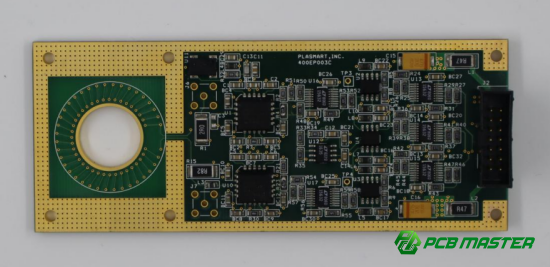
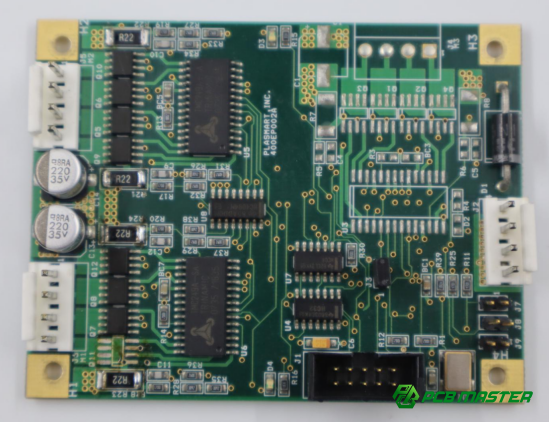
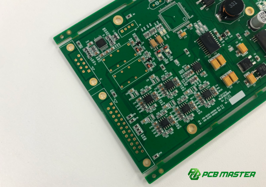
SMT (Surface Mount Technology) plays a crucial role in modern PCB (Printed Circuit Board) design. It allows components to be placed directly onto the surface of the PCB, rather than inserting them through holes. This improves the design by enabling a more compact layout, allowing for smaller devices with more functionality. SMT also supports faster manufacturing processes with automated machines like Pick-and-Place, reducing assembly time and labor costs. The result is higher efficiency, lower cost, and improved overall performance.
How SMT Contributes to Miniaturization and High-Density Circuits
One of the primary advantages of SMT is its contribution to miniaturization. Since SMT components are smaller and require no leads to pass through the board, more components can be placed in the same amount of space. This makes it possible to design smaller and more powerful devices, which is essential in the consumer electronics industry. SMT enables high-density circuits, allowing for complex electronic systems to be packed into tiny devices such as smartphones and wearable technology, without sacrificing performance.
Cost Efficiency of SMT in PCB Production
SMT significantly reduces the cost of PCB production, especially for high-volume manufacturing. Since the assembly process is highly automated, it minimizes human error and reduces the need for manual labor. Additionally, SMT components are generally less expensive to produce than through-hole components because they use less material and are easier to handle during assembly. This cost efficiency makes SMT the preferred choice for mass production, helping to lower the final price of consumer electronics.
Role of SMT in Consumer Electronics
Examples of Products Relying on SMT
SMT has become the backbone of many consumer electronics. Devices like smartphones, laptops, and tablets rely heavily on SMT for their small and compact PCBs. The tiny components used in these devices—such as resistors, capacitors, and integrated circuits (ICs)—are all surface-mounted to save space and enhance performance. Other products like smartwatches, gaming consoles, and even home appliances also depend on SMT to meet the demand for high performance in small packages.
Advantages of SMT in Consumer Electronics
The use of SMT in consumer electronics offers several key advantages. First, it allows for smaller and thinner devices without compromising on functionality. Smartphones, for example, would not be as slim and powerful without SMT. Second, it improves performance and reliability by reducing the risk of mechanical stress and providing better electrical connections. Finally, the cost-effectiveness of SMT helps make high-tech consumer devices affordable to the masses, making advanced electronics accessible to a broader audience. SMT also supports the rapid development and evolution of consumer electronics, as it enables faster production times and quicker product releases.
How Does SMT Work in PCB Assembly?
SMT works in PCB assembly by applying solder paste to the board, placing components with automated Pick and Place machines, and then using a reflow oven to melt the solder, securing the components to the board.
SMT Assembly Process: An Overview
Steps in the SMT Assembly Process
The SMT assembly process involves several critical steps to ensure that the electronic components are properly placed and connected to the PCB. These steps include:
l Solder Paste Application: The first step is applying solder paste onto the PCB using a stencil printer. This paste is a mixture of tiny solder particles and flux, which will later help to bond the components to the board. The stencil ensures the paste is applied precisely where the components will be placed.
l Component Placement: After the paste is applied, the components are placed on the board. Automated machines called Pick and Place machines do this step by picking up the components and placing them accurately on the solder paste. This is a fast and precise process that minimizes human error.
l Reflow Soldering: The final step in the SMT process is reflow soldering. The entire board is heated in a reflow oven, where the solder paste melts and forms solid connections between the components and the PCB. This step requires precise temperature control to ensure the solder forms strong, reliable joints without damaging sensitive components.
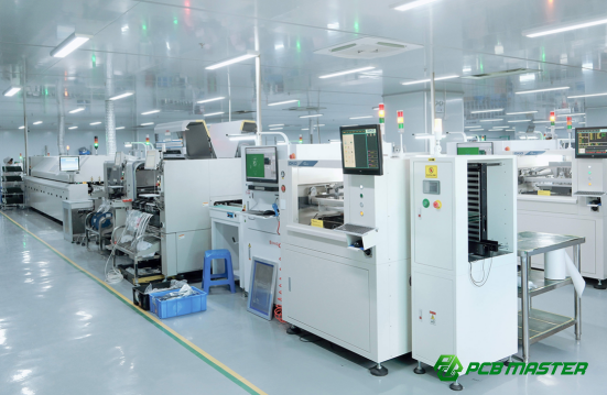
Explanation of Automated Assembly Machines Used
Pick and Place machines are automated systems that accurately pick up tiny components from a feeder tray and place them onto the PCB, all while following a predetermined layout design. These machines are highly efficient, reducing human error and speeding up production. As they operate at high speeds, they ensure that components are placed in the correct position, allowing for high-density and complex designs to be achieved quickly.
Importance of Soldering Techniques in SMT
Soldering is crucial in the SMT process as it creates the electrical connection between the components and the PCB. Proper soldering ensures that there are no cold solder joints, which can lead to electrical failure. The reflow soldering process must be carefully controlled to avoid issues like solder bridges (where solder connects unintended pins) or overheating components. High-quality soldering leads to more reliable and long-lasting electronics.
Key Equipment Used in SMT Assembly
Description of Key Machines: Pick and Place Machine, Reflow Oven, Stencil Printer
l Pick and Place Machine: This machine picks up the SMT components from a tray and places them exactly where they are needed on the PCB. It uses robotic arms and vision systems to ensure accuracy, making it essential for high-speed, high-precision assembly.
l Reflow Oven: The reflow oven is used to melt the solder paste and ensure the components are securely attached to the PCB. The oven heats the board in a controlled way, ensuring the solder melts evenly and forms strong connections without damaging sensitive components.
l Stencil Printer: A stencil printer applies a precise amount of solder paste to the PCB before the components are placed. The stencil, which is a thin metal sheet with holes corresponding to the component pads, ensures that the right amount of paste is applied in the correct locations. This step is critical for ensuring the quality of the solder joints.
How These Machines Contribute to SMT Efficiency and Accuracy
These machines work together to make the SMT assembly process efficient, accurate, and reliable. The Pick and Place machine ensures components are placed in the correct position, even for small or irregularly shaped components. The Reflow oven guarantees that the soldering process is uniform and that the components stay intact, ensuring a strong electrical connection. Finally, the Stencil printer ensures that the solder paste is applied evenly and precisely, preventing defects during the soldering process. Together, these machines minimize human error, increase production speed, and ensure high-quality, consistent results in mass production.
What Are the Components Used in SMT?
The components used in SMT include resistors, capacitors, and integrated circuits (ICs), all designed to be mounted directly onto the surface of a PCB for compact, efficient, and reliable electronic assemblies.
Common SMT Components and Their Characteristics
Description of Typical SMT Components
SMT components are small, flat, and designed to be mounted directly onto the surface of a PCB. The most common types include:
l Resistors: These are components that limit the flow of electric current in a circuit. In SMT, resistors are available in small, flat packages, often in sizes like 0603, 0805, and 1206.
l Capacitors: Capacitors store electrical energy temporarily and release it when needed. SMT capacitors are also small and flat, typically seen in ceramic types, which are often used in high-frequency circuits.
l Integrated Circuits (ICs): ICs are collections of electronic components (like transistors, resistors, and capacitors) within a single package. SMT ICs include microchips and processors found in almost every modern electronic device, ranging from tiny chips to large multi-pin packages.
How SMT Components Are Designed to Work with Surface Mounting
SMT components are designed to be mounted on the surface of the PCB, which differs from traditional through-hole components that require holes for insertion. These components typically have flat leads or pads on the bottom that make direct contact with the PCB's surface. SMT components are made smaller and more robust, allowing for higher component density on the board. This design makes it easier to achieve smaller, more compact electronic devices, like smartphones and wearable gadgets, while improving production speed and reliability.
Types of SMT Packages
Overview of Common SMT Packages
There are several types of packages for SMT components, each designed to suit different needs in terms of size, functionality, and ease of manufacturing. Here are the most common types:
l QFP (Quad Flat Package): A square or rectangular package with leads on all four sides. It is commonly used for chips with many pins and is suitable for higher-density applications like microcontrollers.
l BGA (Ball Grid Array): This package has pins in the form of small solder balls on the bottom. BGAs are used for high-performance chips, such as processors, because they allow for faster signal transmission and improved heat dissipation.
l SMD (Surface-Mount Device): A general term for any component designed to be placed on the surface of the PCB. SMDs are available in various shapes and sizes, and include resistors, capacitors, diodes, and more.
l SOIC (Small Outline Integrated Circuit): A small, flat package with leads on both sides. It is commonly used for medium-to-high-density applications, such as memory chips and operational amplifiers.
Differences Between These Packages and When Each Is Used
Here’s a comparison table that clearly highlights the differences between QFP vs BGA and SMD vs SOIC, showing when each package is typically used:
| Aspect | QFP (Quad Flat Package) | BGA (Ball Grid Array) | SMD (Surface-Mount Device) | SOIC (Small Outline Integrated Circuit) |
| Pin Configuration | Leads on all four sides of the package | Solder balls on the bottom of the package | General term for surface-mount components | Leads on both sides of the package |
| Used For | Devices with many pins needing easy manual soldering | High-performance chips requiring fast data processing and heat management | Various components like resistors, capacitors, etc. | Components needing more pins than typical SMDs, like memory chips or operational amplifiers |
| Soldering Difficulty | Easier to solder manually | More difficult to solder, requires advanced equipment | Easier to handle with automated placement | Moderate difficulty, can be hand-soldered or automated |
| Size and Density | Larger, less compact | Smaller footprint, high pin density | Varies by component, typically compact | Smaller than QFP, suitable for medium-density applications |
| Heat Management | Moderate heat dissipation | Excellent heat dissipation due to solder balls | Varies by component type | Better for medium-density designs |
| Performance | Suitable for general-purpose applications | Preferred for high-speed, high-performance chips | General-purpose, used for low-to-medium complexity | Suitable for devices requiring more pins but not high-performance |
| When to Use | When many pins are needed and manual soldering is required | When high-speed processing and heat management are critical | General use in a variety of applications | When medium-density, compact designs with more pins are needed |
What Are the Advantages of Using SMT?
The advantages of using SMT include improved performance and reliability, cost savings through smaller components and higher density, better heat dissipation, and faster, more efficient manufacturing through automation.
Enhanced Performance and Reliability of SMT Assemblies
How SMT Improves the Performance and Longevity of Electronic Devices
SMT (Surface Mount Technology) significantly enhances the performance and longevity of electronic devices. By using smaller components and placing them directly on the surface of the PCB (Printed Circuit Board), SMT enables tighter circuit designs with shorter signal paths. This reduction in path length helps improve the speed at which signals travel through the board, resulting in faster performance and more reliable data transmission. Additionally, since SMT components are smaller and more precisely mounted, they are less susceptible to mechanical stress, which helps improve the longevity of the device.
Advantages in Terms of Signal Integrity and Heat Dissipation
SMT provides better signal integrity compared to traditional through-hole technology. The components are placed closer together, reducing the possibility of signal degradation over longer paths. Additionally, SMT enables better heat dissipation. Since components are placed directly on the surface, heat can dissipate more evenly across the PCB, preventing hotspots and reducing the risk of component damage. This is particularly important in high-performance devices like smartphones, laptops, and gaming consoles, where heat management is critical for maintaining optimal performance.
Cost-Effectiveness and Space Savings
Economic Benefits of SMT: Reduced Material Costs and Smaller PCBs
SMT offers significant cost savings in both material and production. Since SMT components are smaller, they require less material to manufacture compared to through-hole components. This results in a reduction in the overall cost of components. Additionally, SMT allows for higher component density on the PCB, meaning fewer boards are needed to achieve the same functionality. This not only saves on material costs but also reduces the amount of space required for assembly, leading to overall cost reductions in the manufacturing process.
How SMT Allows for Compact and Efficient Design in Modern Electronics
SMT enables the creation of smaller and more compact designs. By eliminating the need for holes in the PCB, components can be placed directly on the surface, allowing for a denser arrangement. This compact design is crucial for modern electronics, where there is constant demand for smaller devices with more features. For example, smartphones, tablets, and wearables all benefit from the use of SMT because it allows them to be lightweight, slim, and packed with powerful components. Additionally, this efficient use of space contributes to better battery life and overall device performance.
Increased Manufacturing Speed and Automation
Role of Automation in SMT Manufacturing
One of the key advantages of SMT is its high level of automation. SMT assembly lines are equipped with automated machines like Pick and Place machines, which can place thousands of components per hour with high precision. Reflow ovens also automate the soldering process, ensuring that the solder joints are uniform and reliable. Automation not only speeds up production but also improves the quality and consistency of the final product. This is especially beneficial for high-volume manufacturing, where speed and accuracy are crucial.
Comparison of SMT Production Speed with Through-Hole Technology
SMT production is significantly faster than traditional through-hole technology. While through-hole components require manual insertion into PCB holes and soldering on the opposite side, SMT components are placed directly onto the surface and soldered in one go. Automated Pick and Place machines can place components on the PCB in a fraction of the time it would take for manual assembly. This reduced production time leads to faster turnaround, enabling manufacturers to produce large quantities of products more quickly. As a result, SMT is ideal for industries requiring mass production, such as consumer electronics and automotive industries.
What Are the Challenges and Limitations of SMT?
The challenges and limitations of SMT include difficulties in handling small components, the risk of soldering errors like tombstoning and solder bridges, and its reduced suitability for high-power or high-frequency applications where through-hole technology may be more effective.
Challenges in SMT Assembly
Potential Difficulties in Handling Small Components
One of the primary challenges in SMT is the handling of small components. As SMT components are much smaller and lighter than through-hole components, they can be difficult to manage during the assembly process. Automated Pick and Place machines handle the placement, but manual handling can still be problematic, especially when dealing with tiny or irregularly shaped components. Small components are also more likely to be damaged during the manufacturing process if not handled carefully. The tiny size of these components requires precise equipment and trained operators to prevent mistakes, adding complexity to the assembly process.
Risks of Errors in Placement or Soldering (e.g., Tombstoning, Solder Bridges)
While SMT is highly accurate, errors can still occur during the assembly process. Common issues include tombstoning (where a component lifts off one side during soldering) and solder bridges (where excess solder connects two pins of a component, causing a short circuit). These issues are typically caused by incorrect solder paste application, uneven heating in the reflow oven, or inaccurate placement by the Pick and Place machine. Tombstoning can be particularly challenging for components with asymmetric leads, such as resistors and capacitors. Detecting and fixing these errors adds time and cost to the manufacturing process, making it a significant challenge for high-volume production.
Limitations of SMT in Certain Applications
SMT Limitations in Certain High-Power or High-Frequency Circuits
SMT is not ideal for all applications, particularly in high-power or high-frequency circuits. In high-power applications, such as power supplies or motors, the small size of SMT components can limit their ability to handle large amounts of current. Through-hole components are better suited for these applications because they have stronger mechanical bonds and can handle higher power levels. Similarly, in high-frequency circuits, such as radio-frequency (RF) systems, the physical properties of SMT components can lead to signal loss or interference. The smaller and closely packed components can cause issues with inductance and capacitance, affecting the performance of high-speed circuits.
Comparison with Through-Hole Technology for Specific Use Cases
Through-hole technology is still preferred in certain applications, particularly those requiring durability and high current handling. For instance, through-hole components are often used in military, aerospace, and industrial equipment where reliability and mechanical strength are critical. Additionally, through-hole technology offers better heat dissipation in high-power scenarios and is easier to repair and modify in some cases. While SMT offers higher component density and smaller footprints, through-hole technology remains a more robust solution for circuits where size and miniaturization are not the main concerns.
What Are the Different Types of SMT?
The different types of SMT include traditional SMT, 3D SMT for compact, high-density designs, and micro-electronics for ultra-small components, each serving specific applications based on complexity, size, and performance needs.
Surface Mount Technology Variants
Overview of Different SMT Variants
SMT has evolved significantly over the years, with different variants designed for specific needs. Beyond traditional SMT, advanced SMT includes innovations like 3D SMT and micro-electronics:
l Traditional SMT: Involves the standard process where components like resistors, capacitors, and ICs are mounted on the PCB surface. It’s widely used for most consumer electronics and industrial products.
l 3D SMT: This variant involves stacking components on multiple layers, effectively creating a 3D structure. This allows for even more compact and high-density designs, often used in cutting-edge technologies like medical devices, wearable electronics, and space-constrained applications.
l Micro-electronics: This is an advanced form of SMT that involves ultra-small components, often at the micro or nano scale. It is used in high-performance electronics like smartphones, hearing aids, and even miniature sensors.
Key Differences in Manufacturing Processes and Applications
The key differences in manufacturing between these variants largely come down to the level of complexity and the precision required:
l Traditional SMT is easier and more cost-effective to produce, with a straightforward process involving automated machines for placement and soldering.
l 3D SMT requires advanced equipment capable of handling multi-layer stacking and more precise alignment. The manufacturing process is more complex and costly, but it allows for ultra-compact designs that can fit into small, space-restricted devices.
l Micro-electronics manufacturing involves more delicate handling and advanced techniques to work with tiny components, often requiring specialized equipment like laser placement systems.
Comparison Table
| SMT Variant | Components | Manufacturing Process | Applications |
| Traditional SMT | Resistors, capacitors, ICs | Standard automated assembly, soldering | Consumer electronics, automotive, appliances |
| 3D SMT | Stacked components | Advanced multi-layer stacking, precision alignment | Medical devices, wearables, compact electronics |
| Micro-electronics | Ultra-small resistors, capacitors, ICs | Micro-level placement, laser machines | Smartphones, hearing aids, sensors |
Emerging Trends in SMT Technology
Advances in Miniaturization: Chip-on-Board (COB) Technology
Miniaturization has been a key trend in SMT, and one of the most significant developments is Chip-on-Board (COB) technology. COB places an IC directly onto the PCB, allowing for an even more compact design. This technology eliminates the need for traditional packaging of chips, saving both space and material costs. COB is especially useful in products where size is a critical factor, such as LED lighting, medical devices, and portable electronics. It also helps to improve the electrical performance of devices by reducing the length of connections between the chip and PCB.
The Impact of IoT and AI on Future SMT Development
The rise of the Internet of Things (IoT) and Artificial Intelligence (AI) is driving the evolution of SMT in new and exciting ways. As IoT devices become more ubiquitous, there is an increasing demand for smaller, more efficient components. SMT technology will need to keep up with these demands by enabling smaller, high-performance devices. AI, on the other hand, is accelerating the development of smarter, more autonomous manufacturing processes. This includes advancements in machine learning for quality control, predictive maintenance, and even design optimization, all of which will make SMT manufacturing faster and more efficient.
IoT and AI are also pushing the boundaries of micro-electronics and 3D SMT, as these technologies often require extremely small, high-performance components for sensors, smart devices, and edge computing applications.
How to Choose the Right SMT Components for Your PCB?
To choose the right SMT components for your PCB, consider factors like component size, type, voltage rating, placement for optimal signal flow and heat dissipation, and ensure high-quality components for reliability and long-term performance.
Factors to Consider When Selecting SMT Components
Size, Type, and Voltage Rating of Components
When selecting SMT components for your PCB, the size is crucial. Smaller components are typically used for compact designs, while larger components are selected when more power or better heat dissipation is required. The type of component (resistor, capacitor, IC, etc.) depends on the specific function of the circuit. For example, capacitors are used for filtering or energy storage, while resistors limit current flow. The voltage rating of each component must also match the requirements of your circuit to prevent damage or failure. Choosing components with the right voltage rating ensures safe operation and improves the reliability of the PCB.
Importance of Component Placement on the PCB
The placement of components on the PCB plays a major role in both performance and reliability. Proper placement ensures efficient signal flow, reduces interference, and improves heat dissipation. For example, placing high-power components away from sensitive components can prevent overheating. Similarly, ensuring that high-frequency components are kept away from noisy power sources can improve the overall signal integrity of the PCB. Thoughtful placement is especially critical in designs with high-density layouts, where there is limited space for components.
Component Quality and Its Impact on Reliability
The quality of the components used in SMT directly impacts the reliability and longevity of the final product. High-quality components are less likely to fail due to issues like poor solder joints, temperature cycling, or physical stress. Poor-quality components can lead to premature device failure, reduced lifespan, and even safety risks in certain applications. When selecting SMT components, it's essential to choose reputable manufacturers that provide components with high tolerance and stability ratings. Ensuring consistent quality throughout the manufacturing process can significantly reduce maintenance costs and improve the overall performance of the device.
Best Practices for Selecting SMT Components in High-Density PCBs
Tips for Optimizing Component Placement
In high-density PCBs, optimizing component placement is critical to ensure performance, reduce costs, and meet size constraints. A few best practices include:
1. Group similar components: Place components that perform similar functions close to each other to reduce trace lengths and improve signal integrity. For instance, power components should be placed near the power input, and signal components near the signal source.
2. Consider thermal management: Heat-sensitive components should be placed away from heat-generating components, and adequate vias or heat sinks should be used to dissipate heat effectively.
3. Maintain proper spacing: Even in high-density layouts, leaving enough space between components is necessary to avoid short circuits, especially when the PCB undergoes thermal expansion during operation.
4. Use layer stacking: In multi-layer PCBs, placing components on different layers helps to save space and improve the routing of traces.
Tools for Simulating and Designing SMT Components in PCB Layout Software
To optimize component placement and ensure a reliable design, designers often use PCB layout software like Altium Designer, KiCad, or Autodesk Eagle. These tools offer advanced simulation features to test the placement of components and the routing of traces before physical production begins. They can simulate the behavior of the PCB under various conditions, such as heat, voltage, and signal integrity, allowing designers to catch potential issues early in the design phase. Using these tools can help optimize space, improve component placement, and reduce the likelihood of errors during manufacturing. Some software also offers automated design suggestions to improve component placement based on pre-set rules and best practices.
Conclusion
Surface Mount Technology (SMT) has revolutionized the electronics manufacturing industry, offering numerous advantages such as smaller component sizes, faster production speeds, and enhanced performance in modern devices. By allowing for more compact and efficient PCB designs, SMT has made it possible to create high-performance consumer electronics, from smartphones to wearables. The ability to automate assembly processes further reduces costs, improves reliability, and accelerates the production cycle, making SMT the go-to choice for high-volume manufacturing.
Looking to the future, SMT technology will continue to evolve with advances in miniaturization, 3D assembly techniques, and integration with emerging technologies like IoT and AI. As demand for smaller, faster, and more reliable devices grows, SMT will play an increasingly important role in meeting these challenges, supporting the development of next-generation electronics.
For companies aiming to harness the full potential of SMT in their products, partnering with an experienced PCB manufacturer is crucial. PCBMASTER stands out as a trusted supplier, dedicated to delivering high-quality PCBs and PCBA services. With a strict focus on controlling SMT processes and workflows, PCBMASTER ensures that every product meets the highest standards of quality and reliability, helping clients bring their innovations to life with confidence.
FAQs
1. What are the key differences between SMT and through-hole technology?
The key differences between SMT and through-hole technology lie in the way components are mounted on the PCB. In SMT, components are placed directly on the surface of the PCB and soldered, eliminating the need for holes in the board. This allows for smaller, more compact designs. Through-hole technology, on the other hand, involves inserting component leads through holes in the PCB and soldering them on the opposite side, which typically results in larger, more robust designs suited for high-power or high-reliability applications.
2. How does SMT contribute to smaller and more efficient PCB designs?
SMT enables smaller and more efficient PCB designs by using smaller components that are mounted directly onto the surface of the board, allowing for a denser layout. Without the need for holes, more components can be packed into the same area, which reduces the overall size of the PCB. Additionally, the shorter distance between components helps improve signal integrity, reducing the risk of interference and signal degradation. This compactness is essential for modern electronics, where space is limited, and high functionality is required.
3. What are the most common issues faced during SMT assembly, and how can they be avoided?
Some common issues faced during SMT assembly include tombstoning (where one side of a component lifts during soldering), solder bridges (when excess solder creates a short circuit between pins), and misalignment of components. These problems can be avoided by ensuring proper solder paste application, using automated pick-and-place machines for accurate placement, and controlling the reflow soldering process to prevent uneven heating. Additionally, regular inspection using techniques like X-ray or AOI (Automated Optical Inspection) can help detect defects early in the process.
4. Why is SMT important in the manufacturing of consumer electronics?
SMT is crucial in the manufacturing of consumer electronics because it enables smaller, more compact, and cost-effective designs. Modern electronic devices like smartphones, tablets, and wearables require efficient use of space while maintaining high performance. SMT allows for more components to be placed on a smaller PCB, leading to slimmer devices with enhanced features. Additionally, SMT's automated processes speed up production, reduce costs, and ensure consistent product quality, all of which are important for the high-volume production of consumer electronics.
5. How do automated machines like Pick and Place machines improve SMT production?
Automated machines like Pick and Place machines improve SMT production by precisely placing components onto the PCB at high speed. These machines are capable of handling a wide range of component sizes and types, ensuring accurate placement without the errors associated with manual assembly. By automating this step, the process becomes faster and more efficient, reducing the time required to assemble a PCB and increasing the overall throughput of the production line. This level of automation also reduces the risk of human error and enhances the consistency and quality of the final product.
Author Bio
Hi, I'm Carol, the Overseas Marketing Manager at PCBMASTER, where I focus on expanding international markets and researching PCB and PCBA solutions. Since 2020, I've been deeply involved in helping our company collaborate with global clients, addressing their technical and production needs in the PCB and PCBA sectors. Over these years, I've gained extensive experience and developed a deeper understanding of industry trends, challenges, and technological innovations.
Outside of work, I'm passionate about writing and enjoy sharing industry insights, market developments, and practical tips through my blog. I hope my posts can help you better understand the PCB and PCBA industries and maybe even offer some valuable takeaways. Of course, if you have any thoughts or questions, feel free to leave a comment below—I'd love to hear from you and discuss further!

