


Copper Foil in PCB Manufacturing: A Complete Guide to Types, Thickness, and Considerations
Copper foil plays a critical role in PCB manufacturing, influencing everything from electrical conductivity to signal integrity. Its properties directly impact the performance, reliability, and efficiency of electronic devices. With various types, thicknesses, and surface treatments available, selecting the right copper foil is essential to meet specific design requirements.
In this guide, we’ll break down the key factors to consider when choosing copper foil for your PCB projects. From understanding the different types to selecting the ideal thickness, this article will help you make informed decisions that align with your project’s technical needs. Whether you’re working on high-frequency circuits or power-intensive applications, the right copper foil is key to achieving optimal performance.
What is PCB Copper Foil and What Role Does It Play?
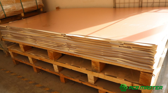
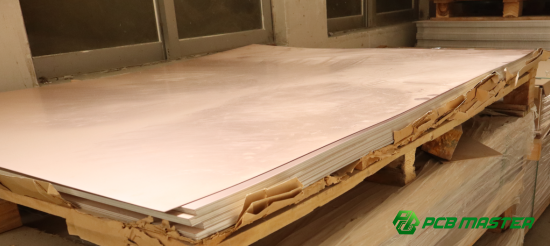
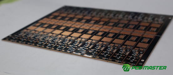
Copper foil is one of the most essential materials in PCB manufacturing. It is typically made from high-purity copper and is bonded to the surface of a PCB substrate, such as fiberglass or resin. Copper foil is extremely thin, usually ranging from a few micrometers to a few millimeters in thickness, and it is used to create electrical circuits on the PCB.
The composition of PCB copper foil consists of copper metal, which is known for its excellent electrical conductivity. This allows electrical signals and power to flow efficiently between components on the PCB. Without copper foil, PCBs would not be able to perform their primary function of connecting and powering the electronic components.
Functions of PCB Copper Foil
The main functions of PCB copper foil are electrical conductivity, signal transmission, and heat dissipation. It ensures that electrical signals flow correctly, supports high-frequency signal transmission, and helps manage heat within the board.
1. Electrical Conductivity:
Copper is one of the best conductors of electricity. In a PCB, copper foil is used to form the electrical pathways, allowing current to flow between components such as resistors, capacitors, and microchips. Without copper foil, it would be impossible to create these necessary electrical connections.
2. Signal Transmission:
Copper foil also plays a vital role in signal transmission, particularly in high-frequency applications. In communication devices like smartphones or computers, the signals need to travel quickly and with minimal loss. The smooth, conductive surface of copper helps transmit these signals more efficiently, making it an essential material for high-speed circuits.
3. Heat Dissipation:
Electronic devices often generate heat as electricity flows through the components. Copper, being an excellent conductor of heat, helps in dissipating this heat away from sensitive areas of the PCB, ensuring that the components do not overheat. This thermal management is critical in maintaining the longevity and reliability of the device.
Real-life Example:
In a smartphone, the copper foil used in the PCB helps connect the CPU, memory, and other components, ensuring that data can be processed efficiently and without interruption. It also helps manage the heat generated by the processor, preventing overheating and ensuring smooth performance.
What are the Main Types of PCB Copper Foil?
The main types of PCB copper foil are classified by manufacturing process (RA Copper Foil and ED Copper Foil) and by application/performance characteristics (Standard, High-Temperature, Low-Profile, Reverse-Treated, and Resin-Coated Copper Foils).
Classification by Manufacturing Process
PCB copper foil is classified into two main types based on the manufacturing process: RA Copper Foil (Rolled Annealed) and ED Copper Foil (Electrodeposited).
RA Copper Foil (Rolled Annealed Copper Foil)
RA Copper Foil is made by rolling copper into thin sheets and then annealing it to soften the material, giving it excellent flexibility and smoothness. It has a low surface roughness, which helps reduce signal loss, especially in high-frequency applications.
Advantages:
l Flexibility: RA copper is highly flexible, making it ideal for flexible printed circuit boards (FPC).
l Smooth Surface: The surface is smooth, with low roughness, which is beneficial for high-speed signal transmission and reducing signal attenuation.
Disadvantages:
l Higher Production Costs: The manufacturing process is more expensive compared to ED copper foil.
l Lower Hardness: RA copper has a softer structure, which may be more prone to scratches and damage during processing.
Main Applications:
l Flexible PCBs (FPC)
l High-frequency and high-speed circuits (e.g., RF/microwave circuits)
ED Copper Foil (Electrodeposited Copper Foil)
ED Copper Foil is produced using an electroplating process, where copper ions are deposited onto a rotating cathode drum, which forms the foil. This type of copper foil is widely used in rigid PCBs, especially in consumer electronics and computers.
Advantages:
l Lower Cost: The manufacturing process is more cost-effective than RA copper foil.
l High Mechanical Strength: ED copper has a higher hardness, making it more resistant to scratches during production.
Disadvantages:
l Less Flexibility: It is not as flexible as RA copper foil, which limits its use in flexible PCBs.
l Higher Surface Roughness: The surface has higher roughness, which may affect high-frequency performance and signal integrity.
Main Applications:
l Rigid PCBs (e.g., smartphones, laptops, and consumer electronics)
l Power electronics and devices with lower flexibility requirements
Comparison Table
| Property | RA Copper Foil | ED Copper Foil |
| Manufacturing Process | Rolling and annealing | Electroplating |
| Flexibility | High (ideal for FPCs) | Low (ideal for rigid PCBs) |
| Surface Smoothness | Low roughness | Higher roughness |
| Cost | Higher | Lower |
| Hardness | Softer (less scratch-resistant) | Harder (more durable) |
| Applications | Flexible, high-frequency, and high-speed circuits | Rigid PCBs, power electronics |
Classification by Application and Performance
PCB copper foil can also be categorized based on its performance characteristics and the specific applications it is best suited for, including standard copper foil, high-temperature and high-ductility copper foil, low-profile copper foil, reverse-treated copper foil, and resin-coated copper foil.
Standard Copper Foil (STD)
Standard copper foil is widely used in most PCB applications, including consumer electronics and general-purpose PCBs. It is produced using the electrodeposition method and provides a reliable, affordable solution for many everyday products.
Advantages:
l Cost-effective
l Sufficient for most general PCB applications
Applications:
l Consumer electronics
l Computer hardware
l General-purpose PCB designs
High-Temperature and High-Ductility Copper Foil (HTE)
HTE copper foil is specially treated to maintain its mechanical properties at elevated temperatures. This makes it ideal for applications where the PCB is exposed to high heat, such as automotive electronics or industrial machinery.
Advantages:
l Good high-temperature resistance
l Prevents cracking under thermal stress
Applications:
l Automotive PCBs
l Industrial machinery
l Devices exposed to heat
Low-Profile Copper Foil (LP/VLP/HVLP)
LP, VLP, and HVLP copper foils are distinguished by their ultra-smooth surfaces, which reduce surface roughness and help minimize signal degradation, making them perfect for high-speed digital circuits and RF applications.
Advantages:
l Extremely smooth surface
l Reduces signal loss in high-speed applications
Applications:
l High-frequency PCBs (e.g., 5G, Wi-Fi, and RF circuits)
l High-speed communication devices
Reverse-Treated Copper Foil (RTF)
RTF copper foil undergoes a special reverse treatment that makes the surface extremely smooth but increases the bond strength between the copper foil and the PCB substrate. This type of foil is used in high-reliability applications where robust adhesion is crucial.
Advantages:
l Improved adhesion
l Strong bond between the foil and substrate
Applications:
l High-reliability PCBs (e.g., aerospace)
l IC substrates
Resin-Coated Copper Foil (RCC)
RCC copper foil has a resin coating applied to one or both sides of the copper, improving adhesion and moisture resistance. This type of copper foil is used in flexible circuit boards (FPCs) and high-performance designs of HDI boards.
Advantages:
l Enhanced adhesion
l Moisture-resistant
Applications:
l Flexible PCBs
l HDI boards
l Wearable devices
l Medical electronics
Comparison Table
| Type | Features | Applications |
| Standard Copper Foil (STD) | General-purpose, cost-effective | Consumer electronics, computer hardware |
| High-Temperature Copper Foil (HTE) | High-temperature resistance, good ductility | Automotive, industrial machinery |
| Low-Profile Copper Foil (LP/VLP/HVLP) | Ultra-smooth surface, reduced signal loss | High-frequency and high-speed circuits |
| Reverse-Treated Copper Foil (RTF) | Enhanced adhesion, smooth surface | Aerospace, IC substrates |
| Resin-Coated Copper Foil (RCC) | Resin coating for moisture resistance | Flexible PCBs, HDI boards, wearable devices |
How to Choose the Right Copper Foil Thickness?
To choose the right copper foil thickness, consider the electrical current requirements, signal integrity needs, and thermal management for your specific application, with thinner foils for high-density circuits and thicker foils for high-current or high-power designs.
Copper Foil Thickness Measurement Methods
Copper foil thickness can be measured in two main ways: by weight (ounces per square foot) or by direct thickness (micrometers or mils).
Weight (Ounces per Square Foot)
The weight measurement system for copper foil is often used in PCB manufacturing. It refers to how much one square foot of copper weighs in ounces. For example, 1 oz per square foot indicates that the copper foil is 35 micrometers thick. This measurement is commonly used because it is simple to relate to copper’s conductivity and thickness in a consistent way.
Conversion:
1 oz per square foot ≈ 35 μm (micrometers).
This method is useful because it directly relates the copper’s conductivity (which depends on its thickness) to its weight.
Real-life Example:
For a mobile phone PCB, the typical copper foil thickness might be 1 oz (about 35 μm), which strikes a balance between flexibility and conductivity.
Direct Thickness (Micrometers or Mils)
Direct thickness measurement uses micrometers (μm) or mils to define the exact thickness of the copper foil. One mil is equal to 0.001 inches, which is approximately 25.4 micrometers. This method gives a precise thickness value without converting from weight, and it’s often used in designs where exact measurements are crucial for performance.
Conversion:
1 mil = 0.001 inches ≈ 25.4 μm.
Real-life Example:
For high-power PCBs used in power supplies, the copper foil might be 2 mils (about 50.8 μm), providing enough thickness to handle the high current flow without overheating.
Common Copper Foil Thickness Specifications
Common copper foil thicknesses include 0.5 oz (~18 μm), 1 oz (~35 μm), 2 oz (~70 μm), and 3 oz (~105 μm+), with each thickness suitable for different applications based on current flow, signal integrity, and power requirements.
0.5 oz (~18 μm)
With a thickness of about 18 μm, 0.5 oz copper foil is often used for high-density interconnects (HDI) where small, fine lines and higher circuit densities are required. This thinner copper is ideal for applications where space is limited, but high conductivity is still necessary. It’s also used in flexible PCBs due to its lighter weight and flexibility.
Applications:
l Mobile phones
l Compact consumer electronics
l HDI boards
1 oz (~35 μm)
1 oz copper foil is the most commonly used thickness for a variety of consumer electronics. It provides enough conductivity for general applications without being too thick or expensive. The 35 μm thickness is ideal for everyday devices, offering optimal performance for power distribution, signal integrity, and heat dissipation.
Applications:
l PCBs for smartphones
l Laptops and computers
l General consumer electronics
2 oz (~70 μm)
With a thickness of about 70 μm, 2 oz copper foil is suitable for circuits that handle higher electrical currents. The thicker foil helps to reduce power loss, improve current-carrying capacity, and dissipate heat more effectively, making it ideal for power-heavy applications like power supplies, motor drivers, and high-power PCBs.
Applications:
l Power supply circuits
l Automotive electronics
l Motor control PCBs
3 oz and Above (~105 μm+)
Copper foils thicker than 3 oz (105 μm+) are used in applications where high power and large currents are present. The increased thickness ensures that the copper can handle higher current densities, provides superior heat dissipation, and reduces the risk of PCB failure due to excessive heat buildup. This type of copper is typically found in high-power electronics and industrial applications.
Applications:
l High-power circuit boards (e.g., electric vehicle battery management systems)
l Heavy-duty power converters
l Automotive power electronics
Comparison Table
| Copper Foil Thickness | Metric Equivalent | Key Characteristics | Typical Applications |
| 0.5 oz | ~18 μm | Very thin, high-density wiring, good flexibility, ideal for fine lines | Mobile phones, compact consumer electronics, HDI boards |
| 1 oz | ~35 μm | Standard balance of conductivity, cost, and performance | Smartphones, laptops, computers, general consumer electronics |
| 2 oz | ~70 μm | High current capacity, better heat dissipation, lower power loss | Power supplies, automotive electronics, motor control PCBs |
| 3 oz+ | ~105 μm+ | Very high current handling, excellent thermal performance, heavy-duty use | EV battery systems, high-power converters, industrial electronics |
Key Considerations for Copper Foil in PCB Design
Key considerations for copper foil in PCB design include its current carrying capacity, impact on signal integrity, impedance control, thermal management, and processability, all of which affect the overall performance and reliability of the PCB.
Current Carrying Capacity
The ability of a PCB to safely carry electrical current depends largely on the copper foil's thickness. Thicker copper foils have a larger cross-sectional area, allowing them to carry more current without excessive heat generation. This is critical for power-intensive applications, where the copper needs to handle high current loads without overheating.
For example, 1 oz copper foil is suitable for low to medium current applications, while 2 oz or 3 oz copper foil is necessary for high-power circuits, such as power supply boards and automotive electronics. The proper copper foil thickness ensures that the PCB can manage the required current while avoiding potential damage or failure due to thermal overload.
Real-life Example:
In a power supply unit, using a thicker copper foil (e.g., 2 oz or 3 oz) helps maintain stable operation by preventing excessive heat buildup during high current flow, which is essential for longevity and reliability.
Signal Integrity
Signal integrity refers to the quality of the electrical signal transmitted through a PCB, which can be influenced by factors such as skin effect and surface roughness of the copper foil.
Skin Effect
At high frequencies, electrical signals tend to concentrate near the surface of the conductor (copper foil), a phenomenon known as the skin effect. This leads to increased resistance and signal loss, particularly in high-speed circuits. The thickness of the copper foil can help reduce the effects of skin effect, as thicker copper can allow signals to travel more efficiently over a larger surface area.
To minimize skin effect, high-frequency PCBs often use low-profile copper foils (LP/VLP/HVLP) with smoother surfaces. This reduces the surface resistance and helps maintain signal integrity, ensuring high-quality transmission.
Real-life Example:
In 5G communication circuits, using copper foil with low surface roughness and adequate thickness helps maintain high-speed signal transmission without loss, which is crucial for data transfer efficiency.
Surface Roughness and Signal Loss
Copper foil with a rough surface can cause additional signal loss as the signal path becomes uneven, leading to higher resistance and greater energy dissipation. Surface roughness is particularly important in high-frequency applications where the signal's integrity must be preserved over long distances.
Low-profile (LP) or very low-profile (VLP) copper foils have smoother surfaces and are ideal for high-speed circuits, as they minimize resistance and reduce signal loss. Choosing the right copper foil with controlled surface roughness can improve overall performance and reliability, particularly in sensitive electronics such as RF and microwave circuits.
Real-life Example:
In a high-frequency PCB used in Wi-Fi routers, using smooth copper foil ensures that the signal remains strong and stable, providing better range and performance.
Impedance Control
Impedance control is essential for maintaining the performance of high-speed digital and RF circuits. Impedance is influenced by the width of the copper traces, the copper foil thickness, and the dielectric material used. A consistent copper foil thickness helps ensure uniform impedance across the PCB, which is crucial for signal integrity in high-frequency applications.
For example, 50 ohms or 100 ohms differential impedance is required in many communication systems. By carefully controlling the copper foil thickness and the trace width, manufacturers can ensure that the impedance remains consistent and the signal is transmitted without distortion or reflection.
Real-life Example:
In a high-speed data transmission PCB, ensuring proper impedance control with accurate copper foil thickness helps prevent data corruption and ensures smooth communication between devices.
Thermal Management
Copper is an excellent conductor of heat, and thicker copper foils can dissipate heat more efficiently. In high-power PCBs, such as those used in power supplies or automotive applications, managing heat is essential to prevent component failure. Copper foil helps carry the heat away from the sensitive areas of the PCB and distributes it evenly across the surface.
The thickness of the copper foil plays a direct role in how effectively the PCB can handle the heat generated by power devices. Thicker copper foils (e.g., 2 oz or 3 oz) can help improve the heat dissipation capability, making them ideal for applications with high thermal demands.
Real-life Example:
In an electric vehicle battery management system (BMS), thicker copper foils help manage the heat generated by the battery, ensuring safe and efficient operation of the system.
Processability
Copper foil thickness impacts the ease and quality of PCB manufacturing processes, such as etching and adhesion to the substrate.
Etching Process
During the etching process, copper foil is chemically removed to create the desired trace patterns. Thicker copper foils take longer to etch, which can increase the time and cost of production. Additionally, thicker copper requires more precise etching control to avoid issues like uneven traces or undercutting, which can affect the performance and reliability of the PCB.
For designs with fine features or high-density interconnects (HDI), thinner copper foils are preferred because they are easier to etch with high precision.
Real-life Example:
For HDI boards used in smartphones, thinner copper foils (e.g., 0.5 oz) are used to ensure precise etching and prevent errors in the delicate, high-density trace patterns.
Peel Strength
Peel strength refers to the bond between the copper foil and the PCB substrate. If the copper foil is not properly bonded, it may peel off during handling or under thermal stress. Thicker copper foils may have different peel strength requirements compared to thinner ones, and ensuring proper adhesion is essential for the PCB's reliability.
Special treatments such as reverse-treated copper foil (RTF) can enhance the peel strength and improve adhesion, making the PCB more durable in harsh environments.
Real-life Example:
In aerospace PCBs, where high mechanical stress is common, high peel strength ensures that the copper foil stays intact and maintains reliable electrical connections under extreme conditions.
What Are the Common Surface Treatment Methods for PCB Copper Foil?
Common surface treatment methods for PCB copper foil include Hot Air Solder Leveling (HASL), Electroless Nickel/Immersion Gold (ENIG), Immersion Tin, Immersion Silver, and Organic Solderability Preservative (OSP), each offering unique benefits for different PCB applications.
Hot Air Solder Leveling (HASL)
Hot Air Solder Leveling (HASL) is one of the most common and traditional methods used to treat PCB copper surfaces. In this process, the copper surface is coated with a layer of molten solder, which is then leveled using hot air to ensure a smooth, even finish. This treatment helps prevent oxidation of the copper, making the surface suitable for soldering components.
Advantages:
l Cost-effective
l Reliable for most standard applications
l Protects the copper from oxidation
Disadvantages:
l Solder layer thickness may be inconsistent
l Not ideal for fine-pitch components or high-frequency applications due to the potential for surface irregularities
Applications:
l Consumer electronics
l Low-to-mid-range PCBs
Real-life Example:
HASL is widely used in smartphone circuit boards and basic consumer electronics, where cost-efficiency is important, and the performance requirements aren't overly demanding.
Electroless Nickel/Immersion Gold (ENIG)
Electroless Nickel/Immersion Gold (ENIG) is a popular surface treatment where a layer of nickel is deposited on the copper surface, followed by a thin layer of gold applied through immersion. This process creates a flat, smooth surface, ideal for high-precision soldering.
Advantages:
l Excellent flatness and smoothness, which is crucial for high-density interconnects (HDI)
l Superior corrosion resistance
l Ideal for fine-pitch components and high-frequency applications
Disadvantages:
l More expensive than HASL
l Requires a more complex process
Applications:
l High-performance PCBs (e.g., mobile devices, high-speed computers, medical devices)
Real-life Example:
ENIG treatment is commonly used in server motherboards and smartphone PCBs, where high-speed, reliable signal transmission is critical.
Immersion Tin
Immersion Tin is a process where a thin layer of tin is deposited on the PCB's copper surface by chemical immersion. This creates a smooth and uniform coating, which is resistant to oxidation, ensuring long-lasting durability for the PCB.
Advantages:
l Cost-effective compared to gold-plating methods
l Smooth surface with minimal oxidation
l Suitable for soldering with a variety of solder types
Disadvantages:
l Susceptible to the formation of tin whiskers, which can cause short circuits in certain conditions
l May not provide the best corrosion resistance compared to other methods like ENIG
Applications:
l Consumer electronics, automotive PCBs, low-to-mid-range applications
Real-life Example:
Immersion tin is often used in automotive electronics like car audio systems and dashboard PCBs, where reliable soldering and cost-efficiency are crucial.
Immersion Silver
Immersion Silver is similar to immersion tin but uses silver as the coating material. Silver offers excellent conductivity and corrosion resistance, making it a great choice for applications where high-quality signal transmission is necessary.
Advantages:
l Excellent solderability and surface smoothness
l Good conductivity
l Corrosion-resistant, especially for longer shelf-life PCBs
Disadvantages:
l Silver can tarnish over time, especially in high-humidity environments
l Not as durable as gold for long-term storage
Applications:
l High-frequency PCBs like RF modules, wireless devices, and high-speed data transmission boards
Real-life Example:
Immersion silver is commonly used in wireless communication PCBs where low signal loss and high reliability are essential.
Organic Solderability Preservative (OSP)
Organic Solderability Preservative (OSP) is an environmentally friendly coating that protects the copper surface of a PCB from oxidation. It is a thin organic layer that preserves the solderability of the copper, ensuring high-quality solder joints. OSP is a popular choice for PCBs that don’t need the durability of more expensive coatings like ENIG.
Advantages:
l Environmentally friendly (no heavy metals like lead or gold)
l Low-cost solution
l Great for standard applications without the need for additional durability
Disadvantages:
l Less durable than other treatments (e.g., ENIG or HASL)
l Limited shelf-life, as it can degrade over time
Applications:
l Consumer electronics, low-cost PCB designs, smart home devices
Real-life Example:
Low-cost electronics like LED lighting systems and home appliances often use OSP as a protective coating for the copper in the PCB due to its low cost and environmental benefits.
Comparison Table
Surface Treatment Key Features Advantages Disadvantages Typical Applications HASL Solder layer applied with hot air Cost-effective, simple Inconsistent solder layer, not ideal for fine-pitch General-purpose, consumer electronics ENIG Nickel + gold plating Excellent flatness, corrosion-resistant, ideal for fine-pitch Expensive, complex High-performance PCBs, mobile devices Immersion Tin Tin plating via immersion Smooth finish, cost-effective Susceptible to tin whiskers Automotive electronics, low-to-mid-range PCBs Immersion Silver Silver plating via immersion Excellent solderability, good conductivity Silver tarnishing over time High-frequency, wireless, RF PCBs OSP Organic coating Environmentally friendly, cost-effective Shorter shelf life, less durable Low-cost, consumer electronics
| Surface Treatment | Key Features | Advantages | Disadvantages | Typical Applications |
| HASL | Solder layer applied with hot air | Cost-effective, simple | Inconsistent solder layer, not ideal for fine-pitch | General-purpose, consumer electronics |
| ENIG | Nickel + gold plating | Excellent flatness, corrosion-resistant, ideal for fine-pitch | Expensive, complex | High-performance PCBs, mobile devices |
| Immersion Tin | Tin plating via immersion | Smooth finish, cost-effective | Susceptible to tin whiskers | Automotive electronics, low-to-mid-range PCBs |
| Immersion Silver | Silver plating via immersion | Excellent solderability, good conductivity | Silver tarnishing over time | High-frequency, wireless, RF PCBs |
| OSP | Organic coating | Environmentally friendly, cost-effective | Shorter shelf life, less durable | Low-cost, consumer electronics |
How to Choose the Right Copper Foil Type for Specific Application Needs?
To choose the right copper foil type for specific application needs, consider factors like electrical performance (current carrying capacity, signal integrity) and mechanical requirements (flexibility, heat resistance) to match the PCB’s functional demands.
Principles for Selecting Copper Foil
When selecting copper foil for a PCB, two primary factors should be considered: electrical performance and mechanical properties. Electrical performance involves ensuring that the copper foil has sufficient conductivity to handle the current and signal integrity needs of the circuit. Mechanical requirements focus on the strength, flexibility, and heat resistance needed for the PCB to function under different environmental conditions.
l Electrical Performance: Choose copper foil with appropriate thickness for the current carrying capacity (e.g., thicker copper for high-current applications like power supplies).
l Mechanical Needs: Consider whether the PCB needs to be flexible or rigid. Flexibility is crucial for flexible PCBs (FPCs), and rigidity is important for rigid PCBs used in consumer electronics or computers.
The key to choosing the right copper foil is balancing these two considerations to meet your specific application needs.
Practical Recommendations for Copper Foil Selection
Practical recommendations for copper foil selection include using low-profile copper for high-frequency PCBs, thicker copper for high-power applications, and high-ductility copper for low-temperature environments to meet specific performance and durability needs.
High-Frequency PCBs
High-frequency PCBs require copper foils with low surface roughness to reduce signal loss due to the skin effect and improve overall signal integrity. The LP (Low Profile), VLP (Very Low Profile), and HVLP (High Very Low Profile) copper foils are ideal for these applications as they offer smooth surfaces and reduce the resistance encountered by high-frequency signals.
Additionally, thinner copper foils, such as 0.5 oz or 1 oz, are commonly used in high-frequency circuits, ensuring better electrical conductivity without unnecessary weight or resistance.
Real-life Example:
In 5G network equipment, using VLP copper foil ensures that high-speed signals are transmitted with minimal attenuation, allowing the equipment to function optimally at very high frequencies.
High-Power PCBs
High-power applications, such as power supplies or motor drivers, require thicker copper foils to handle higher currents. 2 oz (about 70 μm) or 3 oz (about 105 μm) copper foils are ideal for these types of PCBs, as they provide better current-carrying capacity and heat dissipation. Additionally, surface treatments like HASL (Hot Air Solder Leveling) or ENIG (Electroless Nickel/Immersion Gold) are recommended to enhance solderability and provide protection against oxidation, ensuring that the connections remain stable under high temperatures and heavy usage.
Real-life Example:
Automotive electronics, especially in electric vehicle charging circuits, require 3 oz copper foil to ensure the board can handle the large currents and dissipate the heat generated during charging.
Low-Temperature Applications
In environments with extreme temperature fluctuations, copper foils need to maintain both flexibility and strength. High-Temperature Extensible Copper Foil (HTE) is an excellent choice for such applications. HTE copper foils retain their ductility and flexibility even at low temperatures, making them ideal for environments where the PCB might experience rapid temperature changes or must operate at sub-zero temperatures.
Moreover, choosing copper foils with high thermal conductivity will ensure that heat can be efficiently dissipated, preventing damage to sensitive components.
Real-life Example:
In outdoor sensor systems used in arctic environments, HTE copper foil is chosen for its ability to remain flexible and reliable under freezing temperatures, ensuring long-term functionality.
Conclusion
Selecting the right copper foil for your PCB is essential for ensuring optimal performance, reliability, and durability. Whether it's for high-frequency circuits, high-power applications, or low-temperature environments, the choice of copper foil directly impacts the functionality of your PCB. As a seasoned PCB and PCBA supplier, PCBMASTER is dedicated to providing high-quality products tailored to meet your specific needs, helping you build efficient and reliable electronic solutions. Trust us to deliver the materials and expertise that will bring your projects to life.
FAQs
What is the difference between PCB copper foil and copper sheet?
PCB copper foil is a thin layer of copper material used in printed circuit boards (PCBs) primarily for electrical conductivity, while copper sheet is a thicker copper material typically used in industrial applications such as construction, roofing, and electrical wiring. Copper foil is specifically designed for creating circuits in PCBs, offering the necessary properties like flexibility or rigidity depending on the application, while copper sheet is used for broader industrial purposes requiring thicker, more durable copper.
How to choose the right copper foil thickness?
When selecting copper foil thickness, several factors must be considered, including the PCB's current-carrying capacity, signal integrity, and heat dissipation requirements. Thicker copper foils (e.g., 2 oz or 3 oz) are necessary for high-power applications to handle larger currents and provide better heat dissipation, while thinner copper foils (e.g., 0.5 oz or 1 oz) are suitable for general-purpose PCBs or high-frequency applications. The thickness choice will also depend on the complexity of the circuit and whether flexibility is required.
Why is the surface treatment of copper foil important?
Copper foil surface treatment is crucial because it prevents oxidation and improves solderability, directly impacting the PCB's reliability and longevity. Treatments like HASL (Hot Air Solder Leveling), ENIG (Electroless Nickel/Immersion Gold), and OSP (Organic Solderability Preservative) not only protect the copper from environmental degradation but also provide smooth, uniform surfaces for better component attachment. This ensures that the PCB can withstand mechanical stress and perform effectively in its intended application.
Which copper foil is suitable for high-frequency PCBs?
High-frequency PCBs require copper foils with low surface roughness, such as VLP (Very Low Profile) or LP (Low Profile) copper foils. These types of copper foils help minimize signal loss caused by the skin effect, where high-frequency signals travel primarily along the surface of the copper. The smoother the surface, the less resistance the signal encounters, ensuring efficient transmission and maintaining signal integrity, which is critical for high-speed and high-frequency applications like telecommunications and wireless devices.
How does the thickness of copper foil affect PCB performance?
The thickness of copper foil plays a significant role in determining the PCB's electrical and thermal performance. Thicker copper foils increase the current-carrying capacity, enabling the PCB to handle higher power loads without overheating. Thicker copper also improves heat dissipation, which is vital for high-power applications like power supplies and motor drivers. On the other hand, thinner copper foils are better for high-density, high-frequency circuits where signal integrity and reduced resistance are more critical. Too thin or too thick copper can lead to poor performance, heat buildup, or reduced signal integrity, impacting the overall reliability of the PCB.
Author Bio
Hi, I'm Carol, the Overseas Marketing Manager at PCBMASTER, where I focus on expanding international markets and researching PCB and PCBA solutions. Since 2020, I've been deeply involved in helping our company collaborate with global clients, addressing their technical and production needs in the PCB and PCBA sectors. Over these years, I've gained extensive experience and developed a deeper understanding of industry trends, challenges, and technological innovations.
Outside of work, I'm passionate about writing and enjoy sharing industry insights, market developments, and practical tips through my blog. I hope my posts can help you better understand the PCB and PCBA industries and maybe even offer some valuable takeaways. Of course, if you have any thoughts or questions, feel free to leave a comment below—I'd love to hear from you and discuss further!


