


Smart Home PCB and EMS Solutions: What You Need to Know for Success
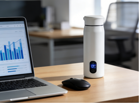
The rapid growth of the smart home market has transformed everyday living, with devices becoming more connected, intuitive, and compact. But behind every successful smart home product lies a complex engineering process—one that starts with the fundamental building blocks: the Printed Circuit Board (PCB) and the Electronic Manufacturing Services (EMS). These crucial components not only enable device functionality but also define how well a product will perform, how long it will last, and how efficiently it can be produced. Making the right choices in PCB design and selecting the right EMS partner can mean the difference between a breakthrough product and a costly failure. As smart home devices continue to evolve, understanding these key factors is essential for creating reliable, cost-effective, and market-ready solutions.
The Importance of PCBs and EMS in Smart Home Products
The Role of PCBs and EMS in Smart Home Product Development
Printed Circuit Boards (PCBs) are the foundation of smart home devices. They are thin boards made of insulating material that house electrical components and connect them with conductive pathways, allowing signals and power to flow between components. Every smart home device—from smart thermostats to security cameras—relies on a well-designed PCB to ensure functionality and performance. A good PCB can make a device more reliable, efficient, and capable of integrating with other devices in a network.
On the other hand, Electronic Manufacturing Services (EMS) are the companies that handle the assembly and production of these PCBs. They ensure that the devices are manufactured with high quality, meet safety standards, and are ready for mass production. EMS providers handle tasks like sourcing materials, assembling components, testing, and ensuring compliance with regulations. The right EMS partner ensures that a product gets to market quickly, at the right quality, and at the right price.
Key Challenges Smart Home Manufacturers Face
Smart home manufacturers face a range of challenges that influence their decisions regarding PCB and EMS selection. These challenges include:
Compact Design: Smart home devices need to be small and unobtrusive, fitting into everyday objects without taking up much space. A well-designed PCB ensures that components are packed efficiently, with no unnecessary extra space. For example, a smart lightbulb requires a PCB that’s both tiny and powerful enough to handle sensors, wireless connectivity, and power management.
Energy Efficiency: Many smart home products, like smart thermostats and wireless sensors, need to run on low power to save energy and extend battery life. The design of the PCB and the efficiency of the EMS play a huge role in ensuring that the device consumes as little power as possible. For instance, a smart thermostat designed for energy efficiency needs a PCB that helps minimize energy use while still providing the required functionality.
Wireless Integration: Connectivity is a must for smart home products, whether it’s Wi-Fi, Bluetooth, ZigBee, or another wireless standard. Ensuring reliable, low-latency communication between devices is essential. A well-designed PCB integrates wireless modules seamlessly, ensuring smooth interaction with smartphones, home hubs, or other smart devices. Consider smart locks, which need to communicate with your phone or central hub via Bluetooth or Wi-Fi. Poor PCB design can lead to connectivity issues, making the device unreliable.
Regulatory Compliance: Smart home devices must adhere to various safety, environmental, and technical regulations, including certifications like RoHS, UL, and CE. These certifications ensure that products are safe, environmentally friendly, and do not emit harmful interference. For example, smart plugs in the U.S. need UL certification to ensure they meet electrical safety standards, while smart cameras sold in Europe must comply with CE certification for electromagnetic compatibility (EMC). Both PCBs and EMS providers must be knowledgeable about these standards to ensure compliance.
By understanding these challenges, manufacturers can make more informed decisions about the PCBs and EMS providers they choose, ensuring their products meet the demands of consumers and regulatory bodies alike.
Understanding the Core Requirements for Smart Home PCBs & EMS Solutions
Essential Characteristics of Smart Home Products
Compact and Space-Efficient Design
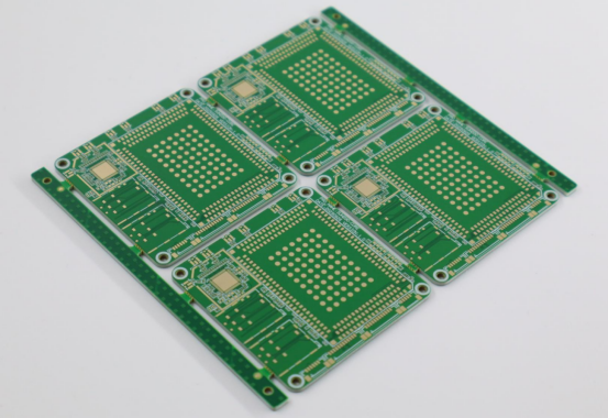
Smart home devices are often designed to fit into small spaces, whether it’s a smart thermostat that sits on a wall or a smart bulb that fits into a light socket. The design must be compact without sacrificing performance. PCBs play a crucial role here. By using multi-layer designs, HDI (High-Density Interconnect) technology, and rigid-flex PCBs, manufacturers can create more space-efficient devices. This allows a range of components—like sensors, microcontrollers, and wireless modules—to fit in a small area without compromising functionality.
For example, a smart doorbell requires a small PCB to fit inside a narrow housing. A good PCB design allows it to carry all the necessary components (camera, microphone, motion sensors) while keeping the device compact and lightweight.
Wireless Connectivity (Wi-Fi, Bluetooth, ZigBee, etc.)
Wireless communication is key for smart home products. Devices need to interact with phones, hubs, and other devices. The most common wireless standards used are Wi-Fi, Bluetooth, ZigBee, and Z-Wave. A well-designed PCB integrates these wireless modules and ensures smooth data transmission.
For instance, a smart speaker requires both Wi-Fi for high-speed internet access and Bluetooth for short-range communication with devices. The PCB needs to support these connections without causing interference, which requires careful placement of components and routing of signal paths. If wireless connectivity is not properly integrated, the device could experience dropouts or poor range, frustrating users.
Energy Efficiency and Thermal Management
Smart home devices, especially battery-powered ones like smart sensors and wireless cameras, must be energy-efficient to extend battery life. Energy efficiency starts with the design of the PCB, where low-power components and energy-saving features are integrated. For example, power management ICs can be used to minimize energy consumption when the device is idle.
Thermal management is equally important. Devices like smart routers or security cameras generate heat during operation. Without proper heat dissipation, the device could overheat, leading to malfunctions or shorter lifespans. PCBs manage thermal issues by using thermal vias (tiny holes that transfer heat away from sensitive components) and copper pours (large copper areas that help spread the heat evenly across the board).
Safety, Durability, and Regulatory Compliance
Safety and durability are non-negotiable for smart home products. Regulatory standards, such as UL certification (for safety) and RoHS (for environmental friendliness), ensure that the device meets safety guidelines. For example, smart plugs need to be UL-certified to ensure they don’t overheat and cause fires. PCBs are designed to comply with these safety standards, using high-quality materials that can withstand heat and electrical stress.
Durability is also a consideration—smart devices often live in harsh environments (e.g., outdoor security cameras must withstand rain and temperature extremes). PCBs designed for these conditions use conformal coatings to protect against moisture, dust, and corrosion.
Key Roles of PCB & EMS in Smart Home Devices
How PCBs Enable Miniaturization, Reliability, and Integration
PCBs are the heart of smart home devices. They allow multiple components—such as microcontrollers, wireless modules, and sensors—to be integrated into a single, compact platform. This miniaturization is critical for smart home products, as it enables the creation of small, lightweight devices.
For example, in a smart thermostat, the PCB houses the temperature sensors, Wi-Fi modules, and control circuits. By integrating these components on a single PCB, the device remains small and efficient while delivering powerful functionality. Additionally, PCBs ensure the reliability of the device. A well-designed PCB can handle power surges, prevent overheating, and ensure long-lasting performance.
Moreover, integration allows for system-on-chip (SoC) solutions, where multiple functions (e.g., processing, connectivity) are combined into a single chip, saving space and reducing the overall cost of the device.
The Role of EMS in Assembly, Testing, and Supply Chain Management
EMS providers play a critical role in ensuring that the PCBs and other components are properly assembled and tested. The EMS partner works closely with the PCB designer to ensure that the design can be manufactured correctly at scale, meeting quality standards.
1. Assembly: EMS providers handle the placement of components on the PCB. They use machines like pick-and-place machines to place components quickly and accurately. For example, in a smart lightbulb, the EMS provider will ensure that all components (LEDs, sensors, Wi-Fi chips) are placed correctly on the PCB, avoiding misplacements that could cause functionality issues.
2. Testing: Once the PCB is assembled, the EMS provider conducts various tests to ensure the device works as intended. These tests may include Automated Optical Inspection (AOI) to check for physical defects, X-ray inspection for hidden defects, and functional testing to ensure the device performs its required functions (e.g., a smart lock unlocking when the app is used).
3. Supply Chain Management: EMS providers also handle sourcing and managing components, ensuring that the right materials are available at the right time. Smart home products often rely on a complex network of suppliers, especially for components like sensors, microcontrollers, and wireless modules. An EMS partner ensures the supply chain remains stable, avoiding production delays and shortages of critical components.
For example, a smart speaker might require a combination of Wi-Fi chips, microphones, and speakers. The EMS provider ensures these parts are sourced from reliable suppliers, and that the assembly line has everything needed to produce the device in large quantities.
Selecting the Right PCB Design for Smart Home Devices
Choosing the Correct PCB Layer Count for Compactness & Functionality
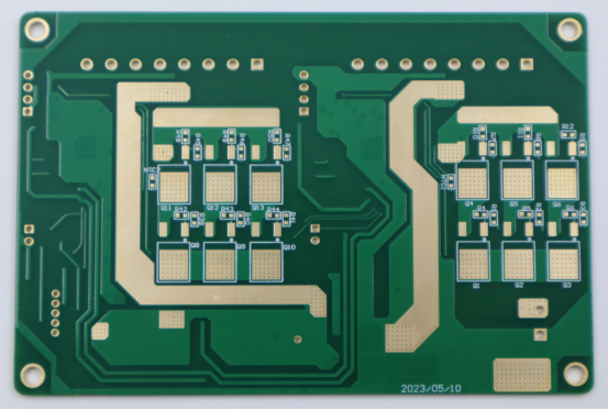
Overview of 6-8 Layer PCBs: Benefits for Space-Saving and Complexity Management
The number of layers in a PCB determines how much space is available for placing components and wiring. Smart home devices often require compact designs that maximize the use of space. A 6-8 layer PCB is ideal for many advanced smart home devices because it balances the need for more space with the limitations of compact housing.
6-layer PCBs: These are typically used for devices with moderate complexity, such as smart speakers. They can integrate various components, including wireless modules, processors, and sensors, without taking up too much space. The added layers allow for more components to be integrated without increasing the device's size.
8-layer PCBs: These are used in high-performance devices like smart cameras or smart routers. More layers allow for advanced routing and the integration of more complex circuits, such as high-speed wireless modules and high-definition cameras.
Choosing the Right Layer Count for Different Device Categories
Different smart home devices require different PCB designs based on their complexity and functionality. Here’s a breakdown of typical PCB layer choices for popular smart home devices:
Single-layer PCBs: Simple devices like motion sensors or basic smart plugs often use single-layer PCBs. These devices have fewer components and simpler functions, so a single layer is sufficient.
Double-layer PCBs: These are used for mid-range devices such as smart bulbs or Wi-Fi-enabled thermostats. Double layers provide a good balance between space and cost, with enough room for basic sensors and wireless connectivity.
6-layer PCBs: Used in more complex devices such as smart speakers, where multiple components like voice recognition chips, Wi-Fi, and Bluetooth modules are integrated into a compact design.
8-layer PCBs: Best for high-performance devices like security cameras or smart routers, where advanced features such as high-resolution video streaming, complex processing units, and multiple wireless bands are required.
Pros and Cons of Single-Layer vs. Multi-Layer Designs in Smart Home Devices
Single-layer PCBs:
Pros: Simpler, lower cost, easier to manufacture, suitable for low-complexity devices.
Cons: Limited space for components, not ideal for advanced functionality like wireless communication and multiple sensors.
Multi-layer PCBs:
Pros: More space for components, better for complex devices with integrated wireless, high-speed data processing, and advanced features.
Cons: Higher cost, more complex to manufacture, may require advanced manufacturing techniques.
Choosing the right PCB layer count depends on the specific needs of the device. A smart lightbulb doesn’t need as many layers as a smart security camera because the former is simpler in design.
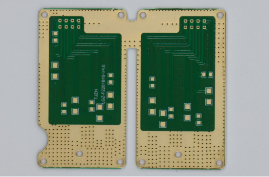
High-Density Interconnect (HDI) Technology
Why HDI is Crucial for Miniaturization in Devices like Smart Wearables and Smart Speakers
HDI technology is used in PCBs to fit more components into a smaller space. This is crucial for devices that need to be compact but still perform advanced functions, such as smart wearables or smart speakers.
HDI PCBs use microvias (tiny holes) and fine-pitch components to increase the number of connections in a smaller area. For example, in a smart speaker, HDI allows the integration of multiple technologies like voice recognition, Wi-Fi, and Bluetooth on a small board, all while maintaining high performance. Without HDI technology, these devices would be too bulky and inefficient.
Techniques for Implementing HDI: Microvias, Fine-Pitch Components, and High-Density Components
Microvias: These are tiny holes drilled in the PCB to create pathways between layers. Microvias allow for more components to fit within the same physical space, which is essential for miniaturized devices like smart wearables or fitness trackers.
Fine-pitch Components: These are components with very small leads (e.g., 0402 size). Fine-pitch components help maximize the use of available space while maintaining high performance. They are commonly used in smart speakers or smartwatches, where space is tight, but advanced functionality is required.
High-Density Components: Using high-density components like System-on-Chip (SoC) solutions, where multiple functions are integrated into one chip, allows manufacturers to save space and reduce costs. SoCs are commonly used in devices like smart thermostats and smart locks.
By implementing these techniques, manufacturers can create smaller, more powerful devices that meet the growing demand for compact and feature-rich smart home products.
Thermal Management in PCB Design
Importance of Heat Dissipation in Devices Like Smart Routers and Thermostats
Many smart home devices, such as smart routers or smart thermostats, generate heat during operation. If not managed correctly, this heat can cause the device to malfunction, shorten its lifespan, or even create safety risks. Effective thermal management is therefore a critical part of PCB design.
For instance, a smart router that handles multiple wireless signals may generate significant heat. Without proper heat dissipation, the router's performance could degrade, leading to connectivity issues or device failure. Similarly, a smart thermostat that controls heating systems must manage heat well to avoid temperature-related errors.
Solutions: Thermal Vias, Copper Pours, and Strategic Placement of Heat-Sensitive Components
To address heat dissipation, PCBs incorporate several solutions:
Thermal Vias: These are small holes in the PCB that allow heat to transfer from hot components to other areas of the board or to a heat sink. By strategically placing thermal vias under heat-generating components (e.g., processors or power amplifiers), heat can be effectively managed.
Copper Pours: This is the use of large copper areas on the PCB to spread heat evenly. Copper has good thermal conductivity, so copper pours help distribute the heat more efficiently, preventing any one part of the PCB from overheating.
Strategic Placement of Heat-Sensitive Components: Designers place sensitive components, like microcontrollers or sensors, away from heat sources to prevent damage. Additionally, conformal coatings can be applied to protect components from environmental factors that could affect their performance.
By integrating these thermal management techniques, manufacturers ensure that smart home devices remain reliable and perform optimally over time, even in environments that generate significant heat.
Quality Control: Testing & Support Post-Production
Key Quality Control Methods for Smart Home Products
Quality control is an ongoing process that ensures products meet specific standards before they reach consumers. Several testing methods are crucial for smart home devices, particularly those that have complex designs and need to operate reliably in varying conditions. Here’s a breakdown of key QC methods:
Automated Optical Inspection (AOI): Visual Inspection for Solder Defects
Automated Optical Inspection (AOI) is a highly effective method used to detect defects in PCB assembly, specifically looking for issues like soldering errors. During the production of smart home devices, the assembly of tiny components like chips, resistors, and capacitors on a PCB must be flawless. AOI systems use cameras to capture detailed images of the board, inspecting for missing or misaligned components, improper solder joints, and other visible defects.
Why it matters: Small defects, like a solder joint that isn’t properly connected, can lead to device failures. For example, a smart thermostat with faulty soldering might not power on, while a smart speaker could experience intermittent connectivity issues due to a poorly soldered Wi-Fi chip.
Example: An AOI system can automatically check a PCB for defects, helping manufacturers identify problems early in the production process, before moving to the more costly stages of testing and packaging.
X-Ray Inspection: Checking for Internal Faults in HDI Boards
X-Ray Inspection is used to detect hidden defects inside High-Density Interconnect (HDI) PCBs. These PCBs are packed with multiple layers of connections, making it difficult to visually inspect the internal connections and components. X-ray inspection helps to identify issues that cannot be seen on the surface, such as voids in solder joints, misaligned microvias, or hidden cracks in layers.
Why it matters: Devices like smart cameras or wearables that use HDI boards need flawless internal connections to ensure stable performance, especially with high-frequency wireless components.
Example: A smart camera may look fine on the outside, but inside, the solder joint holding a key wireless component might be incomplete. X-ray inspection reveals these faults, helping manufacturers avoid performance issues later.
Thermal and Environmental Testing: Ensuring Durability Under Varied Conditions
Smart home devices are exposed to various environmental conditions, including extreme temperatures, humidity, and dust. Thermal and environmental testing ensures that devices can withstand these conditions without failure. This type of testing simulates real-world scenarios by subjecting the device to temperature fluctuations, moisture, and vibrations.
Thermal Testing: Smart devices like smart thermostats or routers generate heat during operation. Thermal testing ensures that the device can handle heat dissipation without overheating or malfunctioning. For instance, smart routers need to maintain consistent performance, even in hot environments.
Environmental Testing: Devices used in areas with high moisture, such as a smart smoke detector in the kitchen or bathroom, must be tested for moisture resistance. Testing ensures the product doesn't fail when exposed to water, steam, or dust.
Example: A smart speaker might be subjected to thermal cycling, where it is exposed to temperature changes from -40°C to 85°C. This ensures that the device continues to function properly, even in environments like a heated living room or a cooler garage.
Post-Sales Support: Maintaining Product Performance Over Time
Once a smart home device is in the hands of consumers, it’s essential to ensure that it continues to perform reliably and remains up-to-date with evolving needs. Post-sales support helps to keep products functioning optimally, resolve issues, and maintain customer satisfaction. Here are some essential aspects of post-sales support:
Offering Firmware Updates and Over-the-Air (OTA) Software Updates
Firmware is the software that controls the hardware of a smart device. Over time, manufacturers may release updates to improve performance, fix bugs, or add new features. Over-the-Air (OTA) updates allow these firmware updates to be installed remotely, without the user needing to connect the device to a computer.
Why it matters: Devices like smart thermostats or security cameras rely on firmware to control features such as temperature settings, motion detection, or wireless connectivity. Without regular updates, these devices may become outdated or encounter bugs.
Example: A smart thermostat may receive a firmware update that optimizes energy usage based on the user's preferences, or a smart door lock might receive security patches to address vulnerabilities.
Benefits: OTA updates allow manufacturers to fix issues quickly, adding new functionalities without requiring users to replace their devices.
Warranty Programs and Proactive Customer Support Strategies
Offering a warranty program gives customers peace of mind, knowing that they can get support or a replacement if their device fails prematurely. A typical warranty may last between 1-2 years, covering defects in materials or workmanship.
Why it matters: A smart lock or smart bulb might encounter issues due to poor manufacturing or a software bug, leading to customer dissatisfaction. A warranty helps manage these concerns and keeps customers loyal to the brand.
Proactive Customer Support: Beyond a warranty, proactive support involves reaching out to customers to ensure their device is working well, offering troubleshooting tips, and addressing concerns before they escalate.
Example: A company selling smart speakers may proactively send notifications about an upcoming firmware update or remind users to clean their devices to avoid overheating.
Building Long-Term Customer Relationships Through Reliable After-Sales Services
Effective after-sales services go beyond fixing problems. They focus on building long-term relationships with customers by offering valuable services that enhance the customer experience.
Why it matters: Building a positive relationship after the sale leads to higher customer retention, more referrals, and better brand loyalty. Happy customers are more likely to purchase future products or recommend them to others.
Example: A smart smoke detector company may offer reminders when it’s time to replace the device's battery, provide educational content on how to maximize the device's features, or offer discounts for future purchases.
Conclusion
Choosing the right PCB and EMS solutions for smart home products is a critical decision that can significantly impact a product’s success. Key factors like quality, wireless integration, and cost management should always be prioritized to ensure the development of reliable, efficient, and affordable smart devices. High-quality PCBs enable devices to be compact, reliable, and energy-efficient—essential qualities for the fast-paced, competitive smart home market. Additionally, seamless wireless connectivity, whether through Wi-Fi, Bluetooth, or ZigBee, is a non-negotiable feature that makes a product functional in today’s connected world.
A strong, ongoing partnership with a certified and experienced PCB and EMS provider is crucial for long-term success. A trusted partner can offer not just manufacturing services but also valuable insights during the design phase, supply chain management, and post-production support. For instance, working with a reliable PCB supplier like PCBMASTER ensures that your product adheres to the highest quality standards and regulatory requirements, while also offering flexibility to scale production efficiently.
Ultimately, selecting the right PCB and EMS partner isn’t just about short-term cost savings—it’s about investing in the long-term performance and reliability of your product. A strong partnership helps ensure that your devices remain competitive, compliant with global standards, and well-supported for years after they reach the market. The success of your smart home products hinges on making informed, strategic choices at every stage, from design to post-sales support.
FAQs
What certifications should my PCB/EMS partner have for selling a smart home device in the U.S.?
When choosing a PCB and EMS partner for your smart home device in the U.S., it's essential to ensure they have certifications like UL (for safety), FCC (for emissions), and RoHS (for hazardous materials). These certifications guarantee that your product meets the necessary safety standards, does not emit harmful interference, and complies with environmental regulations—ensuring both safety and legal compliance.
How do I choose the best PCB layer count for a smart thermostat?
For a smart thermostat, a 4-layer PCB is typically ideal. This configuration strikes the right balance between space efficiency and the ability to integrate more complex components like sensors and wireless modules, while still maintaining cost-effectiveness. It allows for better signal integrity and heat dissipation, which are crucial for a device that needs to operate reliably in a range of environmental conditions.
How can I mitigate the risks of component shortages in my smart home product?
To mitigate the risks of component shortages, you can implement dual sourcing for key components, meaning you use two suppliers for the same part. It's also wise to stockpile critical parts ahead of time and design for part flexibility, so you can swap in alternative components if a primary part becomes unavailable. Planning for these contingencies can help ensure that your production schedule isn't disrupted by supply chain issues.
What is the most common wireless standard for smart home lighting?
ZigBee is the most commonly used wireless standard for smart home lighting. It is preferred because of its mesh networking capabilities, which allow multiple devices to communicate with each other and extend range. Additionally, ZigBee operates at low power, making it ideal for battery-operated devices like smart bulbs, ensuring they consume minimal energy while maintaining reliable connectivity.
What are the key testing methods to ensure quality for smart home products?
Key testing methods to ensure the quality of smart home products include Automated Optical Inspection (AOI) to detect surface defects like solder issues, X-ray Inspection to identify internal defects in complex HDI boards, and thermal testing to ensure the device can withstand varying temperature conditions without malfunctioning. These tests help identify potential flaws early, reducing the risk of product failure after launch and ensuring customer satisfaction.
Author Bio
Hi, I'm Carol, the Overseas Marketing Manager at PCBMASTER, where I focus on expanding international markets and researching PCB and PCBA solutions. Since 2020, I've been deeply involved in helping our company collaborate with global clients, addressing their technical and production needs in the PCB and PCBA sectors. Over these years, I've gained extensive experience and developed a deeper understanding of industry trends, challenges, and technological innovations.
Outside of work, I'm passionate about writing and enjoy sharing industry insights, market developments, and practical tips through my blog. I hope my posts can help you better understand the PCB and PCBA industries and maybe even offer some valuable takeaways. Of course, if you have any thoughts or questions, feel free to leave a comment below—I'd love to hear from you and discuss further!

