


Package on Package (PoP) Technology: A Comprehensive Overview
The relentless pursuit of smaller, faster, and more powerful devices has pushed traditional electronics to their limits. When shrinking size, every millimeter counts, and every component needs to work harder. That's where an innovative solution quietly makes a difference—stacking chips vertically rather than placing them side by side. This method not only saves valuable space but also enhances performance. It’s a shift that’s reshaping everything from smartphones to wearables, allowing engineers to pack more power into the same footprint. This approach, known as Package on Package (PoP) technology, is unlocking a new era of compact, high-performance electronics.
Introduction to Package on Package (PoP) Technology
What is Package on Package (PoP)?
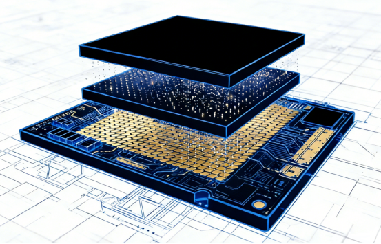
Package on Package (PoP) is a technology that stacks two or more chips vertically in a single module, rather than placing them side-by-side. Typically, a processor (CPU) sits at the bottom, with memory chips (like DRAM) stacked on top. The chips are connected by tiny solder balls, allowing fast data transfer between them.
PoP technology is crucial in compact electronics, like smartphones and wearables, where space is limited. By stacking chips, PoP reduces the overall size of devices while maintaining or improving performance.
Why is PoP Technology Important?
As electronics get smaller, fitting more components in limited space becomes a challenge. PoP solves this by using vertical space, making devices more compact without sacrificing performance. It also reduces signal delay and lowers power consumption, which are key to fast, energy-efficient devices.
In smartphones and wearables, PoP technology improves data transfer speed and extends battery life by shortening the distance between chips.
How PoP Technology Works
Basic PoP Structure: Understanding the Stacked Modules
PoP stacks two or more semiconductor chips vertically in a single module. The bottom chip, usually a processor (CPU), sits at the base, while the top chip, typically a memory module (like DRAM), is stacked on top. These chips are connected by tiny solder balls, allowing fast communication between them. This design reduces device size while maintaining performance, making it ideal for compact electronics like smartphones and wearables.
Example: A smartphone may use PoP to combine a Qualcomm Snapdragon processor and 8GB of LPDDR5 RAM in a compact module, saving space compared to side-by-side chip placement.
PoP Assembly Process: From Start to Finish
The process of assembling PoP modules involves several precise steps to ensure reliability.
Pre-Assembly Preparation
Before assembly, the PCB (printed circuit board) is cleaned to remove dust and contaminants. Solder paste is then applied to the PCB pads, where the chips will sit. Each component is tested to ensure it functions properly before assembly.
Placement of Bottom Package (Logic Core)
The bottom chip (logic core) is placed onto the PCB using a pick-and-place machine. This chip, such as a processor, is carefully aligned with the solder pads on the board. Low-temperature adhesive is used to temporarily hold the chip in place.
Top Package (Memory Module) Alignment
The memory chip is stacked directly on top of the logic chip. The two chips are aligned precisely to ensure the solder balls on the top and bottom packages match up. Accurate alignment is critical for strong, reliable connections.
Reflow Soldering Process
The stacked chips are heated in a reflow oven to melt the solder paste. This creates permanent electrical connections between the bottom and top chips. The temperature is carefully controlled to prevent damage to the components.
Inspection & Testing of PoP Modules
After assembly, the PoP module undergoes X-ray inspection to check for hidden defects, such as missing solder balls or cracks. It also undergoes electrical testing to ensure that data transfers correctly between the chips. Additional thermal tests may be conducted to ensure the module performs well under different conditions.
Key Components of a PoP Stack
Bottom Package (Logic Core)
The bottom package in a PoP stack is typically the logic chip, which is responsible for processing data and controlling the device. This could be a System on a Chip (SoC), like the Qualcomm Snapdragon or Apple A-series chip, or a CPU, such as Intel or AMD processors. These chips perform the heavy lifting, such as running applications, managing tasks, and controlling device functions.
In a PoP configuration, the bottom package is placed on the PCB and serves as the foundation for stacking the memory module on top. The logic chip communicates with the memory chip to run programs and store data quickly.
Top Package (Memory Module)
The top package in a PoP stack is the memory chip, typically either DRAM (Dynamic Random Access Memory) or flash memory. The memory chip stores data temporarily for fast access by the logic chip. DRAM is used for tasks requiring rapid data retrieval, like running apps, while flash memory stores data permanently, like system files and apps.
The top package is stacked on top of the logic chip and connects to it via tiny solder balls or microbumps. The memory module ensures that the processor can access data quickly without delays, enabling smoother performance in devices like smartphones, tablets, and wearables.
Solder Balls: The Connecting Elements
Solder balls are tiny, conductive spheres that connect the top and bottom packages in a PoP stack. These balls are crucial for transmitting data and power between the stacked chips. Typically made of lead-free alloys (like SAC305, which contains tin, silver, and copper), solder balls are placed between the two packages to ensure solid electrical connections.
The size of solder balls can range from 0.06mm to 0.9mm, depending on the type of PoP and the power requirements of the device. The placement method can vary, with the most common techniques being laser jetting, stencil printing, and dispensing. These balls must be placed precisely to avoid short circuits or weak connections.
Advanced Interposers
Interposers are thin layers of material placed between the top and bottom packages in a PoP stack to improve performance, heat management, and signal delivery. These can be made from different materials, including silicon, glass, and organic materials.
Silicon interposers are used in high-performance applications due to their ability to handle a large number of connections and provide excellent heat management. They are typically found in advanced chips like NVIDIA GPUs.
Glass interposers are becoming more common because they offer good heat resistance at a lower cost than silicon, making them ideal for large-scale applications like 5G base stations.
Organic interposers are used in consumer electronics, as they are cost-effective and flexible, making them a good choice for mid-range devices like smartphones and wearables.
Interposers help improve signal integrity, reduce crosstalk (interference between signals), and improve thermal management, ensuring the chips perform reliably at higher speeds and lower power consumption.
Core Benefits of PoP Technology
Space Efficiency
PoP technology significantly reduces the size of electronic devices by stacking chips vertically, rather than placing them side by side. This allows the PCB to occupy less space, which is critical in devices where size matters, such as smartphones, wearables, and compact medical devices.
By stacking components, PoP can shrink the PCB footprint by up to 50%, making it possible to create thinner devices without compromising functionality. For example, a smartphone with PoP technology can have both a processor and memory chip stacked in a small 15mm x 15mm space, saving room for other features like a larger battery or improved camera.
Example: In wearables like the Apple Watch, PoP allows the device to stay compact while providing powerful performance for fitness tracking and notifications.
Performance Enhancement
PoP technology enhances device performance in two important ways: faster data transfer and reduced latency. Since the chips in a PoP stack are placed just a few millimeters apart, data can travel quickly between the processor and memory. This shortens the time it takes to access data, making devices more responsive.
In addition to speeding up data transfer, PoP also reduces power consumption. Shorter signal paths mean there is less electrical resistance, leading to lower energy usage. This efficiency results in longer battery life for portable devices, like smartphones and smartwatches.
Modularity & Flexibility
PoP technology offers modularity—meaning individual chips in a PoP stack can be easily replaced or upgraded without changing the entire system. If the memory module in a device becomes outdated or faulty, you can replace just the RAM without needing to replace the entire processor or motherboard. This makes it easier for manufacturers to offer different configurations of devices, such as upgrading 4GB RAM to 8GB RAM in the same base device.
This flexibility also means that repairs are simpler and less costly. Instead of replacing an entire chip stack, only the faulty component needs to be swapped out, reducing downtime and repair costs.
Cost Savings
While the initial setup for PoP assembly may involve higher costs—due to specialized equipment and testing—the long-term savings are significant. By reducing the PCB size, PoP minimizes material costs, as smaller boards require fewer materials and less complex designs.
Additionally, since PoP stacks multiple chips together, the assembly process is simplified. Fewer soldering steps and smaller footprints mean faster production times, which lowers labor costs. As PoP technology becomes more widely adopted, economies of scale help reduce production costs even further, making it more affordable for manufacturers.
Technological Advancements in PoP
3D PoP: Going Beyond Two Layers
3D PoP is an advanced version of PoP technology that goes beyond just two stacked layers. Using Through-Silicon Vias (TSVs), 3D PoP stacks multiple layers of chips vertically to increase both performance and compactness. Unlike traditional PoP, where only a processor and memory chip are stacked, 3D PoP can stack three or more components—such as CPU, RAM, and storage chips—into a single module.
TSVs are tiny holes drilled through the silicon chips to connect them directly, allowing for faster data transmission between the stacked layers. This reduces signal delay and improves the overall speed of the device. The added layers also optimize the use of vertical space, making it easier to fit more components into smaller spaces without increasing device size.
Hybrid Bonding for Ultra-Low Latency
Hybrid bonding is an innovative technique that uses copper-to-copper connections to bond chips in a PoP stack. Unlike traditional solder ball connections, hybrid bonding provides a direct, low-resistance connection between chips, reducing the time it takes for data to travel between layers. This results in ultra-low latency and more reliable interconnections, which is critical for high-performance devices like gaming consoles, AI processors, and 5G telecom equipment.
By eliminating the delays that come with solder ball connections, hybrid bonding improves overall system speed and efficiency. This technology is especially important for AI and data center applications, where high data throughput and fast response times are crucial.
Innovative Interposers: Glass and Organic Materials
Interposers play a key role in PoP stacks, improving the connection between the top and bottom packages. Traditionally, silicon interposers were used, but newer glass and organic interposers are gaining traction. These materials are cheaper and more heat-resistant than silicon, making them ideal for both high-performance and consumer-grade devices.
Glass interposers are used in applications that require good thermal resistance and high signal integrity, such as 5G base stations and high-bandwidth memory (HBM) modules. Glass is also more cost-effective than silicon, allowing for more affordable solutions in consumer devices like smartphones.
Organic interposers are flexible and lightweight, making them a popular choice for consumer electronics where cost is more important than extreme performance, such as in smartwatches or mid-range smartphones.
Panel-Level PoP (PLPoP)
Panel-Level PoP (PLPoP) is a new manufacturing technique that allows multiple PoP modules to be assembled on a single large panel instead of individually processing each module. This method reduces production time by about 40% and lowers costs by 20%, making it easier to scale production for high-volume devices.
PLPoP is especially useful for mass-produced devices like smartphones, where reducing manufacturing costs and time is critical. This technique is an evolution of wafer-level packaging, which focuses on creating larger PoP modules that can be assembled in a more efficient way.
Co-Packaged Optics (CPO)
Co-Packaged Optics (CPO) is a cutting-edge technology that integrates optical components (like lasers and detectors) directly within a PoP stack. This integration is particularly useful for data centers that require ultra-fast data transmission. By embedding optical components into PoP stacks, CPO enables the transmission of data over fiber optics at extremely high speeds, reducing the need for separate optical modules.
CPO provides higher bandwidth and lower power consumption than traditional electronic interconnects, making it a game-changer for cloud computing and AI processing tasks. This technology is especially important for high-performance computing environments where data needs to be processed quickly and efficiently.
Comparison Table: Technological Advancements in PoP
Technology Key Feature Benefits Use Case Example 3D PoP (With TSVs) Multiple stacked layers with Through-Silicon Vias Higher performance, compact design, faster data transfer High-performance smartphones, gaming devices Hybrid Bonding Copper-to-copper bonding for low-latency interconnections Ultra-low latency, improved reliability, faster connections AI chips in cloud computing, 5G telecom equipment
Glass and Organic Interposers Cheaper, heat-resistant alternatives to silicon interposers Lower cost, better thermal resistance, flexible design 5G base stations, consumer electronics Panel-Level PoP (PLPoP) Mass production using panel-level packaging Reduces production time by 40%, lowers costs by 20% High-volume production of smartphones, wearables Co-Packaged Optics (CPO) Integration of optical components in PoP stacks Higher bandwidth, lower power consumption, faster data transmission Cloud data centers, AI processing tasks
Challenges & Considerations in PoP Implementation
Design and Alignment Precision
One of the biggest challenges in PoP technology is ensuring precise alignment of the stacked chip packages. The stacking process requires specialized machinery to place each chip exactly in the right position, down to micrometers of precision. If the logic chip and memory chip aren’t perfectly aligned, the connections between them can fail, causing malfunction or poor performance.
The alignment process involves advanced machines with high precision capabilities, such as pick-and-place robots and vision systems that use cameras to verify the alignment of the chips before soldering. Even a small misalignment (just 0.1mm) could break the electrical connections, leading to costly defects and malfunctions.
Thermal Management
Heat dissipation is another critical challenge when designing PoP modules, especially as devices become smaller and more powerful. As multiple chips are stacked on top of each other, the heat generated by the logic chip can get trapped, leading to overheating and potential damage to the components. If heat is not effectively managed, it can reduce the lifespan of the PoP module and affect the performance of the entire device.
Advanced materials, such as interposers, help solve these issues by providing better thermal conductivity and spreading heat more evenly across the stack. Silicon, glass, and organic interposers act as buffers to reduce the heat buildup between stacked chips. Additionally, thermal vias—small channels that allow heat to pass from one layer to another—can also be used to dissipate heat more efficiently.
Reliability Under Stress
PoP modules are often used in devices that need to operate under harsh conditions, such as in automotive or medical applications. These environments expose electronics to extreme temperatures, vibrations, and shocks. Ensuring the reliability of PoP technology under such stress is crucial to prevent failure and ensure long-term performance.
To enhance reliability, PoP modules are designed to withstand these stress factors. For instance, automotive-grade PoP uses stronger materials that can handle temperatures ranging from -40°C to 125°C. Similarly, medical-grade PoP modules are tested to endure high vibration and shock resistance to ensure the device performs correctly even when exposed to movement or physical impact.
Conclusion
As devices get smaller and more powerful, PoP technology is becoming a key enabler for high-performance electronics. It offers significant space savings, enhanced speed, and flexibility for manufacturers, making it a go-to solution in industries ranging from smartphones to automotive systems.
To successfully harness the benefits of PoP, precision in design and assembly is crucial. That's where PCBMASTER, a trusted PCB supplier, comes in. With expertise in advanced packaging and cutting-edge manufacturing processes, PCBMASTER ensures your PoP integration is smooth, reliable, and efficient, helping you stay competitive in an ever-evolving market.
FAQs
How does PoP compare to traditional side-by-side chip placement?
PoP technology differs from traditional side-by-side chip placement by stacking chips vertically, allowing for a significant reduction in space usage. This compact stacking also leads to faster data transfer, lower signal delay, and reduced power consumption. In traditional designs, chips are placed side by side, taking up more space and resulting in longer signal paths, which can increase latency and energy usage. PoP reduces these issues, making it ideal for smaller, faster, and more efficient devices.
Can PoP handle the heat in extreme environments?
Yes, PoP technology can handle heat in extreme environments. It is used in demanding applications like automotive and medical devices, where heat resistance and reliability are crucial. Advanced thermal management solutions, such as interposers and thermal vias, help dissipate heat efficiently, ensuring that the stacked chips remain operational even under high temperatures and harsh conditions. This makes PoP an excellent choice for applications that require long-term durability and stability, such as ADAS in vehicles or wearable medical monitors.
What are the main advantages of 3D PoP over standard PoP?
3D PoP technology builds on standard PoP by stacking multiple layers of chips, usually including logic chips (e.g., CPU) and memory (e.g., DRAM) with Through-Silicon Vias (TSVs) for better interconnection. This design offers higher integration, allowing for even smaller form factors and improved performance. The increased number of layers and the use of TSVs reduce the module size even further, resulting in faster data transfer rates and lower latency, making it ideal for high-performance applications like gaming consoles and 5G telecom equipment.
Is PoP technology suitable for consumer devices only?
No, PoP technology is not limited to consumer devices. While it is widely used in smartphones, tablets, and wearables, PoP also plays a critical role in other industries such as automotive, healthcare, telecommunications, and data centers. In automotive, PoP is essential for systems like ADAS, where reliability and speed are paramount. In healthcare, PoP helps fit high-performance chips into compact medical wearables. Additionally, 5G base stations and data center processors use PoP for high-bandwidth and low-latency connectivity.
What are the cost implications of PoP?
While PoP technology can involve higher upfront costs due to specialized equipment and testing, it offers significant long-term savings. These savings come from reduced PCB material costs (due to the smaller size of the PoP module), fewer assembly steps, and the ability to upgrade individual components (such as swapping out RAM chips without replacing the entire module). In high-volume manufacturing, PoP can become more cost-effective than traditional chip packaging over time. Additionally, the modular nature of PoP allows for easier repairs and upgrades, which further reduces costs for manufacturers and consumers in the long run.
Author Bio
Hi, I'm Carol, the Overseas Marketing Manager at PCBMASTER, where I focus on expanding international markets and researching PCB and PCBA solutions. Since 2020, I've been deeply involved in helping our company collaborate with global clients, addressing their technical and production needs in the PCB and PCBA sectors. Over these years, I've gained extensive experience and developed a deeper understanding of industry trends, challenges, and technological innovations.
Outside of work, I'm passionate about writing and enjoy sharing industry insights, market developments, and practical tips through my blog. I hope my posts can help you better understand the PCB and PCBA industries and maybe even offer some valuable takeaways. Of course, if you have any thoughts or questions, feel free to leave a comment below—I'd love to hear from you and discuss further!

