


Rigid-Flex PCBs in Wearables: Advanced Design Challenges and Practical Solutions
The wearable technology market is growing fast. In 2025, it was worth about USD 219.3 billion and is expected to reach USD 493.26 billion by 2030, with a strong growth rate of 17.6% each year. This shows that more and more people are using smartwatches, fitness trackers, medical wearables, and other connected devices in their daily lives.
At the heart of these devices is the printed circuit board (PCB). It acts like the “nervous system” of the device, connecting and powering every part. For many wearables, engineers prefer rigid-flex PCBs instead of traditional rigid PCBs. Why? Because rigid-flex PCBs are thin, lightweight, and can bend or fold to fit inside small, oddly shaped devices. This makes them perfect for wearables, which must be comfortable, reliable, and durable even when people move around.
By understanding why rigid-flex PCBs are so important, we can see how they make modern wearables smaller, smarter, and stronger.
Rigid-Flex PCB Basics and Material Selection
Rigid-Flex PCBs are a smart solution for modern electronics. They combine hard and flexible areas in one board, allowing devices to be smaller, lighter, and more durable. Understanding their structure and materials is key to designing boards that perform reliably in real-world use.
1. Definition and Structure
A Rigid-Flex PCB is a circuit board that integrates both rigid (hard) and flexible (bendable) sections in a single unit. This design allows the board to fit into compact or uniquely shaped devices while maintaining strength where it is needed.
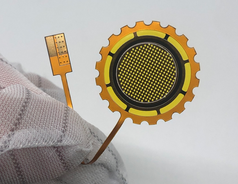
The rigid parts provide a stable base to mount electronic components such as chips, resistors, and connectors. These areas ensure that components stay securely in place and are protected from mechanical stress. Flexible sections, on the other hand, can bend, fold, or twist, connecting rigid parts without extra wires. This not only saves space but also reduces the weight of the device. Flexible areas are commonly used in devices like smartphones, cameras, wearable electronics, and medical devices where movement or compact design is required.
Via connections are small, plated holes that link the rigid and flexible areas. These vias act like bridges, allowing electricity to flow reliably between different layers of the board. Proper via design is crucial to prevent signal loss, maintain electrical performance, and ensure long-term reliability of the board.
2. Material Selection
Rigid Board Materials
FR-4 is one of the most common rigid board materials. It is made from woven fiberglass combined with resin, providing mechanical strength, stability, and electrical insulation. FR-4 can withstand most normal operating temperatures and is suitable for a wide range of applications. High-TG (glass transition temperature) materials are designed to tolerate higher temperatures, which is important during soldering or in devices that generate heat, such as automotive or industrial electronics. These materials prevent warping or damage when the board is exposed to high temperatures.
Flexible Base Materials
Polyimide (PI) is a specialized plastic that is thin, strong, and highly heat resistant. It can bend many times without cracking, making it ideal for flexible sections that fold or twist frequently. Thin copper foil is applied to flexible areas to carry electrical signals. The copper is thin enough to allow bending without breaking the circuit but still thick enough to maintain good conductivity and signal integrity.
Adhesives and Insulating Layers
Special adhesives and insulating layers hold the multiple layers of the board together. They ensure that electricity flows only through the intended paths, preventing short circuits. Some adhesives are flexible, allowing the board to bend without separating the layers. Choosing the right combination of adhesive and insulating material is essential for durability, flexibility, and reliable electrical performance.
3. Thickness Design
Flexible sections: Usually very thin, about 0.1–0.2 mm, so they can bend easily without cracking. Thinner boards bend more easily but are less strong.
Rigid sections: Usually thicker, about 0.4–1.6 mm, to support components and provide mechanical strength. The thickness is chosen depending on how heavy the components are and how much the board needs to resist bending or pressure.
Advanced Design Challenges of Rigid-Flex PCBs
Rigid-Flex PCBs are powerful but complex. Designing them requires careful planning to make sure the board bends without breaking, signals remain strong, and heat and stress are managed effectively. The following sections explain the main design challenges engineers face and how they address them.
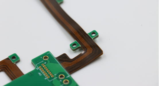
1. Stack-up and Routing Design
When designing a Rigid-Flex PCB, engineers must plan exactly how the rigid and flexible sections connect. The main goal is to reduce stress in the areas that bend. If the layout is poorly planned, the flexible section can crack or the circuit can fail.
To prevent this, engineers carefully stack the layers, including rigid substrates, flexible materials, and copper traces, so that the flexible part can bend safely. Components are placed strategically to avoid putting stress on flexible areas, and the routing of electrical traces is designed to minimize tension during bending. Proper stack-up and routing ensure both reliability and durability, even after repeated use.
2. Signal Integrity (SI) and Electromagnetic Compatibility (EMC/EMI)
Electrical signals in a Rigid-Flex PCB must travel cleanly and reliably, especially in high-speed circuits. Poor design can cause signal loss, reflections, or interference, affecting device performance.
Engineers use specific trace types such as microstrip and stripline, carefully selecting their width, spacing, and placement within the stack-up to control signal behavior. Impedance control is crucial to balance resistance and capacitance, preventing signal degradation. Additionally, via placement is carefully planned because vias—small metal holes connecting layers—can introduce interference or slow down high-frequency signals if positioned incorrectly. Thoughtful SI and EMC design ensures that the board performs reliably in real-world conditions.
3. Thermal Management
High-power chips generate heat that must be removed to prevent damage and maintain performance. Engineers design heat dissipation systems using copper layers and, when necessary, attach heatsinks to spread and remove heat efficiently.
Copper thickness plays a key role: thicker copper can carry more current and distribute heat more effectively. By combining well-designed copper layers with heatsinks, engineers make sure that the chips remain cool, even under heavy processing loads. Effective thermal management prevents failures and extends the life of the PCB and the device.
4. Mechanical Stress and Bend Life
Flexible sections of a Rigid-Flex PCB bend during normal use, so engineers must ensure these areas can survive repeated movement. Dynamic bending occurs when the board flexes repeatedly, such as in folding devices, while static bending occurs when the board is bent once and stays in that position, like a fixed cable.
Engineers calculate the minimum bend radius, which is the tightest curve the flexible section can handle without cracking. Stress analysis is performed to predict how the board will behave under repeated bending or mechanical strain. By optimizing both the material selection and layout, engineers ensure that the board can endure repeated bending over its intended lifespan.
Manufacturing and Assembly Best Practices for Rigid-Flex PCBs
Rigid-Flex PCBs are delicate yet powerful, combining rigid and flexible areas in one board. Proper manufacturing and assembly are essential to make sure these boards perform reliably in real devices. The following best practices explain how engineers carefully place components, test for durability, and maintain quality in every production batch.
1. SMT / Turnkey PCB Assembly
Surface Mount Technology (SMT) is the process where electronic components are mounted directly onto the surface of the PCB. Turnkey assembly means the manufacturer handles the entire process, from component sourcing to final assembly, ensuring a smooth and consistent production.
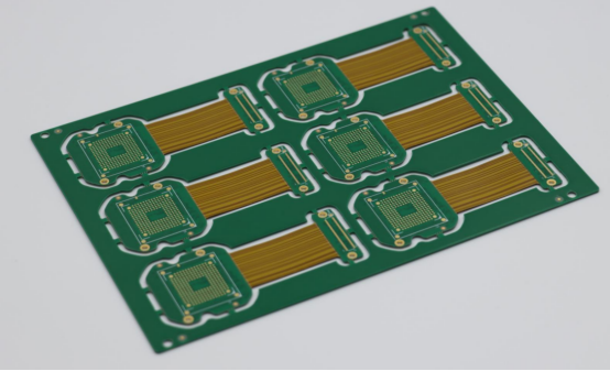
High-density component placement is a major challenge in Rigid-Flex PCBs. Some boards have dozens or even hundreds of tiny components packed very closely together. Engineers must carefully plan the placement to prevent soldering errors, component collisions, or assembly difficulties. Flexible areas require extra attention because they are delicate. During assembly, both machines and human operators must handle these sections carefully to avoid bending, tearing, or damaging the copper traces.
Reflow soldering is used to attach the components securely. The temperature profile during reflow is critical: too hot can damage flexible materials, while too cold may result in weak solder joints. Engineers carefully optimize the heating and cooling curve, ensuring all components are soldered reliably without harming the flexible regions of the board.
2. Testing and Reliability Assurance
After assembly, every board undergoes rigorous testing to ensure functionality and durability. Automated Optical Inspection (AOI) machines examine each board for missing or misaligned components and poor soldering. X-ray inspection is also employed to check hidden layers and internal connections that cannot be seen with the naked eye.
In addition to visual inspections, mechanical and environmental tests are conducted. Bend testing simulates repeated movement, checking whether the flexible areas can survive normal use without cracking or losing conductivity. Thermal cycling exposes the boards to repeated heating and cooling, ensuring they can withstand temperature fluctuations during real-world operation. These tests help catch potential failures early and confirm the board’s long-term reliability.
3. Production Batch Control
Maintaining consistency from prototypes to full-scale production is critical. Engineers establish strict processes to ensure that each board uses the same materials, soldering techniques, and testing procedures. This consistency minimizes variability between boards and reduces the risk of defects.
During production, process controls monitor key parameters such as layer alignment, solder quality, and bending tolerances. Any deviation is corrected immediately to maintain uniformity across all units. By adhering to consistent procedures, manufacturers can deliver large quantities of Rigid-Flex PCBs with predictable quality and high reliability.
Real-World Application Cases of Rigid-Flex PCBs
Rigid-Flex PCBs are everywhere in modern gadgets. From smartwatches to wearable health devices, they bend, fold, and fit into tight spaces while keeping signals reliable. Let’s explore some real examples to see how these boards make everyday electronics possible.
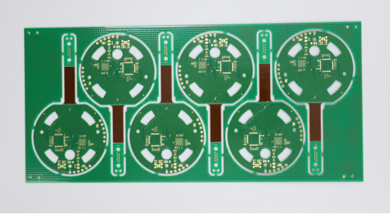
1. Smartwatch Internal PCB Layout
Inside a smartwatch, space is extremely limited. The Rigid-Flex PCB allows the board to wrap around corners and fit into tiny spaces without adding extra wires.
Rigid sections hold the main chips, connectors, and critical components securely. Flexible sections connect the screen, battery, and sensors, providing necessary movement while maintaining reliable electrical connections.
Proper layout reduces mechanical stress on the flexible areas. This ensures that the watch can bend slightly during normal use without breaking the circuits, increasing durability and lifespan.
2. Health Monitoring Patch PCB Design and Bend Point Optimization
Health monitoring patches stick directly to the skin, which means they need to bend and flex constantly as the wearer moves.
Engineers carefully design flexible zones with the right thickness and bend radius so the patch remains comfortable and functional. Special attention is given to the areas that bend the most, called bend points, to prevent cracks, signal loss, or early failures.
This design ensures that the patch can work reliably for long periods, even during daily activities or exercise.
3. Wearable Sports Device High-Density Routing Scheme
Sports devices, like fitness trackers, often contain many sensors and a small battery packed into a tiny case. High-density routing is used to connect all the components without increasing the overall size of the device.
Flexible sections allow the PCB to fold or twist to match the shape of the wearable device, while rigid sections keep the important components secure. This combination ensures that electrical signals remain strong and reliable, even when the device bends during movement.
Conclusion
Rigid-Flex PCBs are evolving fast. The future points to ultra-thin, highly integrated, and foldable designs. Devices will become smaller, lighter, and more flexible, opening new possibilities for wearable electronics, medical devices, and smart gadgets, making technology more convenient and versatile.
When designing Rigid-Flex PCBs, engineers focus on a few key things. Choosing the right materials, carefully planning the routing and layer stack-up, managing heat effectively, and following precise manufacturing processes are all essential. Paying attention to these points ensures the board is strong, reliable, and long-lasting.
For anyone working with Rigid-Flex PCBs, it is important to plan for movement, protect flexible areas, and test thoroughly. A well-designed board not only works better but also lasts longer, giving devices the durability they need in real-world use.
If you have any questions or want to learn more about PCBs, feel free to reach out to PCBMASTER. We are a professional PCB supplier and are happy to assist you.
FAQs
1. Why do wearable devices need Rigid-Flex PCBs instead of traditional rigid PCBs?
Wearable devices are small, light, and often bend or move with the user. Traditional rigid PCBs are hard and cannot bend, so they may break or take up too much space. Rigid-Flex PCBs combine rigid areas to hold components and flexible areas to bend or fold. This design allows the device to fit in tiny spaces, stay light, and survive daily movement. For example, a smartwatch’s screen and battery need to connect through a flexible area without wires, which only a Rigid-Flex PCB can do safely.
2. How do engineers make sure Rigid-Flex PCBs last through repeated bending?
Engineers calculate the “minimum bend radius,” which is the tightest curve the flexible section can handle without cracking. They also choose materials like polyimide that can bend many times without breaking. Components are placed on rigid areas, and flexible zones are carefully routed to avoid stress. In testing, boards are bent repeatedly and exposed to heat changes to make sure they survive real-world use. This ensures that wearable devices, which move with the body, remain reliable over time.
3. What special care is needed during assembly of Rigid-Flex PCBs?
Because Rigid-Flex PCBs have delicate flexible areas, assembly must be precise. Components are placed carefully to avoid touching flexible sections. Machines and humans handle the board gently to prevent tearing or bending damage. During soldering, engineers control the temperature very carefully: too hot can damage flexible materials, too cold can make weak solder joints. After assembly, boards are tested visually and with X-rays to check hidden connections. These steps make sure the PCB works correctly and lasts a long time, even in small wearable devices.

