


Essential Guide to PCB Copper Thickness Choosing the Right Option
Introduction
In PCB design and manufacturing, the selection of copper thickness not only affects circuit performance but is also a critical factor influencing product cost and production cycle. Choosing the right copper thickness can make your project twice as effective with half the effort.
The selection of copper thickness in PCB design is a crucial decision that directly impacts circuit performance, reliability, and cost. Whether for ordinary consumer electronics or high-reliability industrial equipment, appropriate copper thickness ensures optimal balance in current carrying capacity, heat dissipation capability, and mechanical strength.
This article provides a comprehensive analysis of all aspects of PCB copper thickness, from design considerations and cost differences to production cycles, helping you make informed decisions.
Fundamental Concepts of PCB Copper Thickness
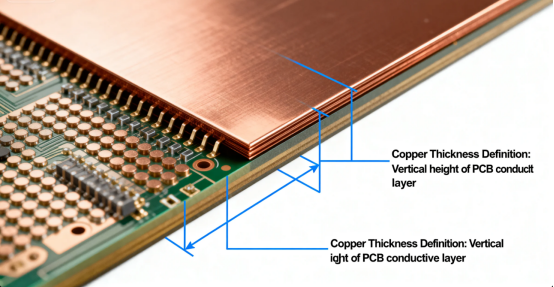
A printed circuit board (PCB) is a board made from a copper clad laminate, which is a laminate material with copper bonded to its surface. PCB copper thickness is typically measured in ounces (oz), where 1oz copper thickness means the copper foil weighs 1 ounce per one square foot (oz/ft²), which is a standard unit of copper weight. Finished copper thickness refers to the final, industry-standard measurement of copper on a PCB after all manufacturing steps. Copper thickness is often measured in mils (thousandths of an inch), with 1oz copper corresponding to about 1.37 mils (0.00137 inch) or approximately 35 micrometers (μm). The thickness of the copper layer is typically specified in inches, mils, or micrometers, and designers must determine the appropriate thickness based on design requirements. Copper thickness is measured by weight and then pressed flat to achieve a uniform copper layer, resulting in a specific thickness. The resulting thickness of copper is determined by spreading a given copper weight over a defined surface area.
Common copper foil thicknesses include: 0.5oz (about 17.5μm), 1oz (about 35μm), 2oz (about 70μm), 3oz (about 105μm), and even thicker options like 4oz (about 140μm) or more. These different copper weights (such as 0.5oz, 1oz, 2oz, etc.) are used for different applications, and these weights impact the electrical and mechanical properties of the PCB. For special applications such as high-power equipment, copper thickness can reach up to 200oz. Copper clad and copper clad laminates are the starting materials for PCB fabrication.
The final copper thickness of a standard PCB consists of the base copper thickness plus the thickness from panel plating (full-board electroplating) and pattern plating (graphic electroplating). The copper layer is built up through plating processes, and the finished copper thickness is specified in design documentation. For example, a standard finished 1oz copper thickness, according to IPC Class 2 standards, typically has primary copper (panel plating) thickness of 5-7μm and secondary copper (pattern plating) thickness of 13-15μm, resulting in hole copper thickness between 18-22μm.
Characteristics and Applications of Different Copper Thicknesses
Standard Copper Thickness (1oz)
1 oz copper thickness (approximately 35μm) is the standard copper weight used in most PCBs. About 70% of circuit boards use 1 oz (35μm) copper foil thickness. It’s suitable for most ordinary electronic products, such as consumer electronics, communication devices, and general control boards.
The advantages of 1 oz copper thickness include processing convenience, lower cost, and mature manufacturing processes. For digital circuits requiring high signal integrity, 1 oz copper thickness also provides good performance.
Heavy Copper Thickness (2oz and above)
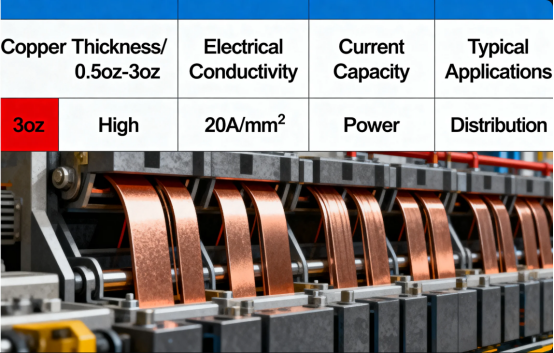
2oz copper thickness (approximately 70μm) and above are primarily used for high-current, high-power, and high-heat dissipation applications. In these scenarios, designers often specify heavier copper and different thicknesses on various PCB layers to meet finished copper weight requirements, optimizing performance, thermal management, and mechanical stability.
Compared to 1oz copper, 2oz copper can carry approximately twice the current at the same trace width. For instance, while 1mm trace width with 1oz copper might carry 23A current, 2oz copper can handle 46A or more. This is particularly critical in high-power applications such as LED driver power supplies, automotive electronics, and motor controllers that require stable high-current transmission.
Thick copper PCBs also provide better thermal performance and higher mechanical strength. With copper’s high thermal conductivity, thicker copper can more effectively transfer heat generated by chips and power components to the board exterior, reducing the risk of local overheating. Additionally, thicker copper increases trace mechanical strength, making them less susceptible to breakage from bending, thermal expansion/contraction, or high-frequency vibration.
Design Considerations for Copper Thickness Selection
Current Carrying Capacity
Copper thickness selection must first consider circuit current requirements. While some formulas can directly calculate maximum current carrying capacity, actual circuit design is more complex. Safety factors must be fully considered in designs. Additionally, temperature rise should be evaluated when selecting copper thickness for high-current traces, as excessive temperature rise can impact safe operation and heat dissipation.
Trace width design must match copper thickness. For 3oz copper foil, recommended trace width is ≥0.2mm with spacing ≥0.25mm to avoid etching residue; for 6oz and above specifications, width should be increased to 0.3mm or more, while using curved corners (radius ≥0.5mm) to reduce current concentration.
Thermal Design
For high-power applications, thermal design must be considered. Thermal vias (diameter 0.6-0.8mm, density ≥5 vias/cm²) should be implemented and directly connected to copper areas, with via pad diameter at least 0.4mm larger than the hole diameter to enhance heat conduction paths.
Thick copper PCBs typically require special lamination processes involving various PP fillers to meet required filling specifications during pressing.
Layer Stack-up and Symmetrical Design
Multilayer ultra-thick copper boards should adopt symmetrical design, with top and bottom layer copper thickness difference ≤1oz, and inner-to-outer layer copper thickness ratio controlled between 1:2-1:3 to balance interlayer stress and reduce warping risk. Copper weight distribution should be balanced so that no one layer has significantly more copper than others, and inner layer copper thickness is managed carefully—typically through print and etch techniques—to ensure board stability.
Internal patterns on PCB substrates have blank areas on each layer; exposed areas have no copper. Additionally, board edges are designed with individual air channels.
Manufacturing Process Limitations
Different copper thicknesses impose different requirements on manufacturing processes. Conventional etching techniques are not ideal for manufacturing heavy copper PCBs, as they produce over-etched edges and uneven edge lines. PCB manufacturers now use advanced etching and plating methods to achieve straight edges. Manufacturers plate copper onto the board to increase copper thickness, and plated copper is essential for meeting design requirements. The plating copper process forms the final copper layer and ensures reliable electrical connections.
Ultra-thick copper boards (3oz and above) require stringent precision and stability in manufacturing processes. In etching processes, since copper foil thickness exceeds 105μm, high-concentration acidic etchants (copper chloride concentration controlled at 180-220g/L) are needed, with dual spray systems, using differential pressure control to reduce side etching and ensure line edge verticality ≥85°. Chemicals and chemical solutions are used to etch away excess copper and define the final copper features.
Cost Differences Between Different Copper Thicknesses
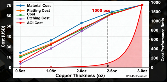
PCB copper thickness is an important factor affecting price. Generally, thicker copper foil leads to higher prices.
Multiple factors influence PCB pricing, including materials, surface finish processes, design complexity, copper foil thickness, quality acceptance standards, mold and test fixture costs, payment terms, order quantity, and delivery time.
From a material cost perspective, increased copper thickness directly raises raw material costs. Additionally, thick copper PCB manufacturing is more complex, with potentially lower yields further increasing costs. PCB fabrication costs also rise with greater copper thickness due to more complex construction of the PCB layers and the larger surface area of copper required.
For prototypes and small batch production, PCB manufacturers typically charge engineering fees (such as flying probe test fees). For volume production, molds and test fixtures are required (mold cost about $110, test fixture about $165), but mass production improves efficiency, actually reducing per-unit production costs.
Surface finish selection also affects overall cost. Common processes include: OSP (anti-oxidation), leaded HASL, lead-free HASL (environmentally friendly), gold plating, ENIG, etc., with prices increasing in this order.
Production Cycles for Different Copper Thicknesses
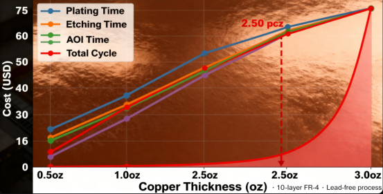
PCB copper thickness also affects production cycles. Generally, greater copper thickness increases production difficulty and may require longer production times.
| PCB Type | Sample Cycle (Expedited) | Sample Cycle (Standard) | Volume Cycle |
|---|---|---|---|
| Single-layer | 12 hours | 2 days | 3 days |
| Double-layer | 24 hours | 3 days | 4 days |
| 4-layer | 48 hours | 4 days | 6 days |
| 6-layer | - | 5 days | 8 days |
| 8-layer | - | 7 days | - |
Below is a reference for approximate production cycles of different PCB types:
Ultra-thick copper boards require longer production cycles due to complex manufacturing processes needing special etching and plating methods. For example, heavy copper PCBs typically require special lamination processes involving various PP fillers to meet required filling specifications during pressing, which takes additional time.
The lamination process requires solving thermal matching issues using step-wise pressure application: maintaining pressure at 0.8-1.0MPa at room temperature stage, increasing to 1.5-1.8MPa at 120°C, stabilizing at 2.0-2.2MPa during 180°C curing stage, while controlling heating rate at 2-3°C/min to avoid substrate warping from thermal stress. These special process requirements all increase production time.
Special Applications: Heavy Copper PCBs and Ultra-Thick Copper Boards
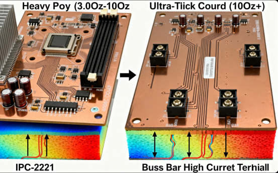
Heavy copper PCBs typically refer to circuit boards with 4 ounces or more copper per layer. 4-ounce copper PCBs are most commonly used in commercial products, with copper concentrations reaching up to 200 ounces per square foot.
These PCBs are widely used in electronics and circuits requiring high-power transmission, such as transformers, heat sinks, inverters, military equipment, solar panels, automotive products, welding equipment, and power distribution systems. Additionally, the thermal strength provided by these PCBs is impeccable, crucial in applications where high temperatures could damage sensitive electronic components.
Ultra-thick copper board manufacturing requires special processes:
·Copper embedding method: This approach uses planes to manufacture thick copper PCBs. Heavy copper is inserted into prepreg resin, with resin thickness determining copper thickness.
·Blue bar method: Thick copper bars are inserted into the circuit board. This method saves materials and reduces PCB weight. During manufacturing, resin flows into spaces inside copper lines, helping achieve a uniform top surface.
When manufacturing heavy copper PCBs, plating copper in holes—such as plated through holes (PTH), blind, and buried via holes—is critical for ensuring electrical connectivity and mechanical strength. Proper copper plating on the hole barrels is essential to meet quality standards and maintain reliable performance.
For multilayer boards with thick copper layers, attention must be paid to copper fill levels between inner layers. Low filler and resin content can lead to insufficient resin.
How to Choose the Right Copper Thickness
Selecting appropriate PCB copper thickness requires considering multiple factors:
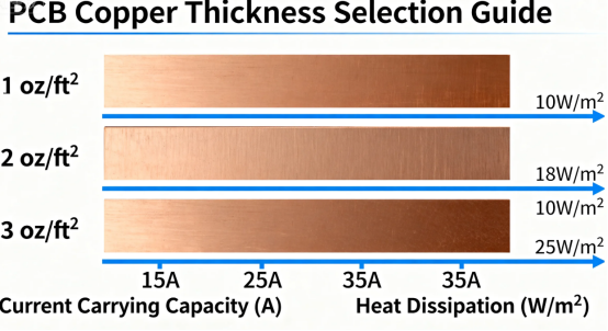
·Current requirements: Choose copper thickness capable of carrying required current based on circuit current levels. High-current applications require thicker copper foil.
·Thermal requirements: Applications with high power density or stringent thermal dissipation requirements need thicker copper foil to improve heat conduction capability.
·Space constraints: When limited space requires carrying high current, increasing copper thickness may be preferable to increasing trace width.
·Mechanical stability: In areas with frequent plugging/unplugging of connectors, long-term stressed pads, or vias prone to impact, thick copper better ensures structural integrity.
·Cost considerations: Balance performance needs and cost constraints to select optimal cost-effective copper thickness.
·Manufacturing process: Consider PCB manufacturer’s process capabilities to ensure they can produce circuit boards with selected copper thickness. Note that gerber files, which are commonly used to communicate PCB design data to manufacturers, do not specify copper thickness. Therefore, you must provide additional documentation such as stackup tables or fabrication notes to clearly indicate the required copper thickness.
Generally, ordinary double-sided and single-sided boards typically use 1oz (35μm) copper thickness. Multilayer boards usually have 35μm outer layers and 17.5μm (0.7mil) inner layers. For PCBs requiring high current, consider using thicker copper foils such as 70μm, 105μm, or even 140μm.
Conclusion
PCB copper thickness selection is an engineering decision requiring comprehensive consideration of multiple factors. It affects not only circuit electrical performance and reliability but also directly relates to product cost and manufacturing cycle.
As electronic devices evolve toward high performance and high density, requirements for PCB copper thickness are becoming increasingly diverse. Understanding characteristics, application scenarios, and design considerations of different copper thicknesses helps engineers make better choices and optimize product design.
Whether choosing standard copper thickness or thick copper design, close communication with PCB manufacturers is essential to ensure designs meet manufacturing process requirements, achieving optimal performance, reliability, and cost-effectiveness.
We hope this article provides comprehensive reference information about PCB copper thickness, helping you make informed decisions in your next project.
Author: Jack Wang

