The Hidden Value of Printed Circuit Board Scrap: Recycling and Recovery Insights
In today’s tech-driven world, printed circuit boards (PCBs) power nearly every electronic device—from smartphones to satellites. Yet, when these boards reach the end of their life, they’re often dismissed as worthless waste. What many overlook is that PCB scrap holds remarkable hidden value, containing recoverable metals and materials that can be turned into profit and sustainability. As the demand for greener production grows, discovering the potential within PCB scrap becomes both a practical and responsible choice.
Understanding the Value in Printed Circuit Board Scrap
What Is Printed Circuit Board (PCB) Scrap?
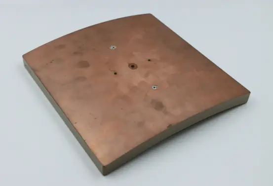
Printed circuit board (PCB) scrap refers to the leftover, defective, or end-of-life circuit boards generated during electronics manufacturing or after consumer products are discarded. These boards serve as the foundation for electronic devices, providing electrical connections between components. Once they are damaged, outdated, or fail quality inspection, they become PCB scrap.
Common sources of PCB scrap include:
Smartphone boards and tablets, often containing fine copper and gold traces.
Computer motherboards and server boards, which are rich in recoverable precious metals.
Industrial and automotive PCBs , which usually contain thicker copper layers and specialized alloys.
PCB scrap can be divided into two main categories :
- Pre-consumer scrap, produced during manufacturing. This includes offcuts, rejected panels, or assembly rejects.
- Post-consumer scrap, which comes from discarded or obsolete electronic products—commonly known as e-waste.
This distinction matters because pre-consumer scrap is usually cleaner and easier to recycle, while post-consumer scrap often requires additional dismantling and separation due to mixed materials and contamination.
Why PCB Scrap Is More Valuable Than It Seems
Although PCB scrap looks like useless debris, it actually contains high-value metals such as gold, silver, copper, palladium, and rare earth elements. These materials are essential for electrical conductivity and manufacturing new electronics.
On average, one ton of high-grade PCB scrap can yield between 100 and 300 grams of gold, along with kilograms of copper and smaller quantities of silver and palladium. By comparison, traditional gold mining typically extracts only 1–5 grams of gold per ton of ore—making PCB recycling nearly 50 times richer in recoverable gold than natural mining.
This surprising ratio explains why PCB recycling is often called “urban mining.” Instead of digging into the earth, recyclers “mine” valuable metals from discarded electronics. Urban mining reduces the need for raw material extraction, cuts down on energy use, and supports the circular economy—an approach where materials are continually reused instead of discarded.
In short, PCB scrap is not waste but a concentrated resource pool that, when processed responsibly, delivers both economic value and environmental sustainability.
Composition of PCB Scrap — What Materials Can Be Recovered?
Printed circuit board (PCB) scrap is made up of both metallic and non-metallic materials. Understanding its composition is essential for designing efficient recycling processes and maximizing material recovery.
Metal Components
The most valuable part of PCB scrap lies in its metal content, which typically makes up 30–40% of the total board weight. These metals are critical for electrical conductivity and play a major role in determining the scrap’s market value.
Common metals found in PCB scrap include:
| Metal | Function in PCBs | Typical Presence | Recovery Value (Approx.) |
|---|---|---|---|
| Copper (Cu) | Main conductive layer and vias | 20–30% | Moderate but high volume |
| Tin (Sn) | Solder joints and coatings | 1–5% | Moderate |
| Gold (Au) | Plating on connectors and contact pads | <0.1% | Very high per gram |
| Silver (Ag) | Conductive coatings and solder alloys | <0.1% | High |
| Nickel (Ni) | Underplating and corrosion resistance | <0.5% | Moderate |
| Palladium (Pd) | Surface finish and multilayer connectors | Trace | Very high per gram |
Key insight: While copper dominates by weight, precious metals like gold and palladium drive most of the economic value. Their excellent conductivity and resistance to corrosion make them indispensable in high-performance electronics.
Recyclers often use mechanical separation followed by chemical or electrochemical extraction to recover these metals efficiently. High-grade PCB scrap—such as that from telecom or aerospace equipment—tends to contain richer concentrations of precious metals compared to consumer electronics.
Non-Metal Components
Beyond metals, PCBs also contain a variety of non-metallic materials that provide mechanical strength and insulation.
Fiberglass (glass fibers) – Reinforces the board and provides rigidity.
Epoxy resin – Binds layers together and offers electrical insulation.
Ceramics – Used in high-temperature or specialized industrial boards for durability.
These materials typically account for 50–60% of PCB weight. While they have limited recyclability, they can still be repurposed or used for energy recovery. For example, crushed fiberglass-resin mixtures can serve as filler in construction materials or be processed in waste-to-energy facilities under controlled conditions.
Proper separation of these materials ensures that the recycling process remains efficient and minimizes contamination during metal recovery.
Hazardous Substances and Environmental Considerations
PCB scrap also contains hazardous substances that require special handling. These may include:
Lead (Pb) – Common in older solder joints.
Brominated flame retardants (BFRs) – Added to prevent fires but can release toxic gases if burned.
Cadmium (Cd) and Mercury (Hg) – Sometimes found in older components and surface finishes.
Improper disposal or open burning of PCB scrap can release toxic fumes and heavy metals into the environment, contaminating soil and water.
Therefore, responsible recycling practices—such as using closed-loop chemical processes, controlled thermal recovery, and compliance with RoHS and WEEE regulations—are essential to ensure environmental safety and worker protection.
The PCB Scrap Recycling Process — Step-by-Step Overview
Recycling printed circuit board (PCB) scrap involves several stages designed to separate valuable metals from non-metallic materials while minimizing environmental harm. Each step—from collection to advanced metal recovery—plays a critical role in achieving efficient, sustainable recycling.
Collection and Sorting
PCB scrap is primarily collected from electronics manufacturers, repair centers, and e-waste recycling facilities.
Pre-consumer sources include defective or excess boards from production lines.
Post-consumer sources come from discarded electronic products such as computers, servers, and communication devices.
Once collected, the boards undergo sorting to classify them by type, size, and metal content.
Manual sorting is still widely used for high-value boards, where experienced workers can visually identify components rich in precious metals.
Automated sorting systems , equipped with optical sensors or X-ray fluorescence (XRF) scanners, detect material composition with high accuracy, improving processing speed and consistency.
Effective sorting ensures that high-value PCB scrap receives specialized treatment while low-grade material is directed to bulk processing, optimizing recovery yields and cost efficiency.
Mechanical Processing
After sorting, the next step is mechanical processing, which focuses on size reduction and material separation.
- Shredding and Grinding – PCBs are first shredded into smaller pieces and then ground into fine particles to expose embedded metals.
- Sieving and Classification – Particles are sorted by size to facilitate separation.
- Magnetic Separation – Magnetic drums or belts remove ferrous metals such as iron and nickel.
- Electrostatic Separation – This technique separates conductive metals (like copper and gold) from non-conductive materials (like fiberglass and resin) using electrical charges.
Mechanical processing prepares the material for further refining. It is an essential pre-treatment step that minimizes chemical use in later recovery stages.
Chemical or Hydrometallurgical Recovery
The hydrometallurgical process relies on chemical reactions to extract metals from crushed PCB material.
Acid Leaching: Solutions containing acids (such as aqua regia or sulfuric acid) dissolve metals from PCB particles.
Electrolysis: The dissolved metals are then recovered through electrochemical deposition, producing pure metal sheets or powders.
Environmental precautions are critical in this step. Waste acid solutions must be neutralized, and heavy-metal residues are filtered before disposal or reuse. Many facilities now employ closed-loop systems that recycle process water and reagents to reduce pollution and chemical costs.
Hydrometallurgy is known for its high metal recovery rate and precision, particularly for precious metals like gold and palladium.
Pyrometallurgical (Thermal) Methods
In pyrometallurgical processing, PCB scrap is treated at high temperatures to melt and separate metals.
Smelting: The boards are heated in furnaces, causing metals to separate based on their melting points.
Incineration and Refining: Organic materials are burned off, leaving metallic residues for further purification.
While pyrometallurgical methods are faster and capable of processing large volumes, they have higher energy costs and produce more emissions than hydrometallurgical recovery.
Comparison:
Efficiency: Pyrometallurgy offers quick bulk recovery; hydrometallurgy achieves higher purity levels.
Cost: Thermal processes are energy-intensive; chemical processes require more reagent management.
Environmental impact: Pyrometallurgy emits more CO₂, while hydrometallurgy produces liquid waste that needs treatment.
Recyclers often combine both approaches—using smelting for base metals and chemical extraction for precious metals—to balance efficiency and sustainability.
Emerging Green Technologies
Modern research is transforming PCB recycling with eco-friendly innovations that reduce chemical and energy use.
Bioleaching: Certain microorganisms, such as Acidithiobacillus ferrooxidans, naturally dissolve metals from PCB scrap by generating mild acids. This method operates at low temperatures and produces minimal waste.
Solvent-Free and Closed-Loop Systems: These processes use mechanical activation, ionic liquids, or supercritical fluids to recover metals without traditional acids or cyanides.
Hybrid Recycling Models: Some facilities integrate AI-driven sorting, low-temperature metal recovery, and energy recovery from resin components, making recycling both profitable and sustainable.
These green technologies represent the future of urban mining—extracting valuable materials from electronic waste with minimal environmental impact.
Economic and Environmental Benefits of PCB Scrap Recycling
Recycling printed circuit board (PCB) scrap offers dual advantages — economic profit and environmental protection. By recovering precious metals and reusing valuable resources, companies can reduce costs, support sustainability goals, and strengthen their role in the global circular economy.
Economic Value and Market Trends
PCB scrap recycling is not just an environmental necessity — it’s a profitable industry driven by the high market value of recovered metals such as gold, copper, silver, and palladium.
Profit potential:
On average, one ton of high-grade PCB scrap can contain 100–300 grams of gold, several kilograms of copper and silver, and traces of palladium.
Based on 2025 commodity prices, the metal recovery value from one ton of PCB scrap can exceed US $10,000–15,000, depending on the composition and efficiency of the recycling process.
Global market trend:
The demand for precious metals continues to rise due to their use in semiconductors, EV batteries, and renewable energy systems.With limited natural reserves, industries increasingly rely on recycling-driven supply chains to meet material needs.
According to recent market analyses , the global E-waste recycling market size is valued at USD 40.27 billion in 2025 and is forecast to reach USD 70.63 billion by 2030, progressing at an 11.89% CAGR over the period, with PCB recycling emerging as one of its fastest-growing segments.
Environmental Sustainability
PCB scrap recycling directly contributes to environmental preservation by reducing electronic waste and conserving natural resources.
Key environmental benefits include:
Reduced e-waste volume: Each ton of recycled PCB scrap prevents approximately 800–900 kg of material from ending up in landfills.
Energy conservation: Extracting metals from recycled boards requires up to 85% less energy compared to traditional mining and refining processes.
Carbon footprint reduction: Recycling one ton of PCB scrap can save approximately 1.5–2 tons of CO₂ emissions, depending on the recovery methods used.
These savings come from avoiding the intensive mining, transportation, and smelting activities involved in extracting metals from ore. By recycling PCBs, manufacturers and recyclers minimize both greenhouse gas emissions and toxic waste generation, advancing global climate goals.
Contribution to Circular Economy
PCB recycling is a cornerstone of the circular economy, where materials are continuously reused instead of discarded. This approach keeps valuable resources in circulation and minimizes the need for new raw material extraction.
Key connections to the circular economy:
Material reuse: Recovered metals from PCB scrap re-enter manufacturing supply chains for electronics, automotive, and renewable energy industries.
Resource efficiency: Recycling maximizes the utility of existing materials, reducing dependence on virgin mining.
Responsible manufacturing: Companies that adopt PCB recycling align with international sustainability standards and ESG (Environmental, Social, and Governance) frameworks.
Regulatory alignment: PCB recycling also supports compliance with global environmental directives, including:
RoHS (Restriction of Hazardous Substances) — limits toxic materials in electronics.
WEEE (Waste Electrical and Electronic Equipment Directive) — promotes collection and recycling of e-waste in the EU.
ISO 14001 environmental management systems — encourages sustainable resource use.
By integrating PCB scrap recycling into their operations, businesses strengthen their supply chain resilience, enhance brand reputation, and contribute to a closed-loop production model that benefits both industry and the planet.
Challenges and Future Opportunities in PCB Scrap Recovery
While PCB scrap recycling offers significant economic and environmental benefits, the industry faces multiple technical, regulatory, and operational challenges. Addressing these challenges opens the door to innovations and future growth in the recycling sector.
Technical and Operational Challenges
Recycling printed circuit boards is technically complex due to the intricate design and material composition of modern PCBs.
Complex multilayer boards: Many PCBs consist of 10, 20, or more layers, making it difficult to separate metals from resin and fiberglass. The tiny embedded traces of gold, palladium, and copper require precise mechanical or chemical treatment.
Variation in PCB composition: Different electronic devices use boards with varied metal concentrations and non-metallic materials. For example, smartphone PCBs may be rich in gold but low in copper, while industrial PCBs have thicker copper layers but fewer precious metals. This variability affects recovery efficiency and requires adaptable recycling methods.
These challenges demand advanced processing techniques, careful sorting, and highly controlled operations to maximize material recovery while minimizing waste and contamination.
Regulatory and Supply Chain Barriers
The PCB recycling industry is also shaped by legal frameworks and logistics constraints.
Differences in international e-waste standards: Countries enforce different regulations for collection, recycling, and disposal of PCB scrap. Compliance with RoHS, WEEE, Basel Convention, and local environmental laws is critical but can be complex for cross-border operations.
Logistics and export/import restrictions: Transporting PCB scrap to recycling facilities can be costly and subject to strict monitoring. Shipping hazardous waste internationally often requires documentation, permits, and adherence to environmental safety protocols, adding to operational costs.
These barriers can slow down recycling operations and limit access to high-grade scrap, highlighting the need for efficient domestic recycling infrastructure and standardized international practices.
Innovations and Future Directions
Emerging technologies and policy developments are creating opportunities to overcome existing challenges and enhance PCB scrap recovery.
AI-driven sorting and robotics: Machine learning and computer vision systems can automatically identify high-value boards and components, while robots dismantle devices with precision, reducing labor costs and contamination.
Advanced metal recovery techniques: New chemical and thermal methods improve extraction efficiency, reduce chemical use, and increase recovery of precious metals like gold and palladium.
Digital tracking for recyclable materials: Blockchain or IoT-enabled systems track PCB scrap through collection, processing, and final recovery, improving transparency and regulatory compliance.
Investment and policy incentives: Government subsidies, tax breaks, and public-private partnerships encourage sustainable e-waste management, promoting large-scale adoption of recycling technologies.
These innovations make PCB recycling more efficient, safer, and environmentally responsible, while supporting the growth of a circular economy where valuable metals are continuously reused.
Conclusion — Unlocking the Hidden Potential of PCB Scrap
Recycling printed circuit board (PCB) scrap offers dual benefits: it provides a significant economic return through the recovery of valuable metals like gold, copper, and palladium, while simultaneously supporting environmental responsibility by reducing e-waste, conserving energy, and lowering carbon emissions. Adopting advanced recycling practices, including AI-driven sorting, hydrometallurgical recovery, and green technologies, is essential to maximize efficiency and sustainability.
Collaboration among manufacturers, recyclers, and policymakers is key to overcoming technical, regulatory, and logistical challenges. By integrating efficient recycling strategies, promoting standardized regulations, and investing in innovative technologies, the PCB industry can contribute to a circular economy, turning what was once considered waste into a renewable source of high-value materials.
For those who want to explore PCB materials, recycling methods, or sustainability strategies further, PCBMASTER—as a seasoned PCB supplier— can provide expert guidance and professional solutions tailored to your needs.
FAQs
1. What types of metals can be recovered from printed circuit board scrap?
PCB scrap contains both base metals and precious metals that can be recovered:
Copper (Cu): The main conductive material in PCB traces and layers.
Gold (Au): Found in connectors and contact pads; highly valuable.
Silver (Ag): Used in solder and conductive coatings.
Palladium (Pd): Used in multilayer boards and plating.
Nickel (Ni): Provides corrosion resistance under gold plating.
Tin (Sn): Present in solder layers.
Example: One ton of high-grade PCB scrap can yield 100–300 grams of gold, several kilograms of copper, and small amounts of silver and palladium.
2. How does PCB recycling differ from general e-waste recycling?
PCB recycling is more specialized compared to general e-waste recycling:
Focus on high-value metals: PCBs are rich in precious metals, unlike general electronics waste, which contains more plastics and non-metal components.
Advanced separation processes: PCB recycling uses mechanical shredding, electrostatic separation, chemical leaching, or smelting, while general e-waste may rely on manual dismantling and bulk sorting.
Environmental precautions: PCB recycling requires careful handling of hazardous materials such as lead, brominated flame retardants, and cadmium, which may not be the primary concern in general e-waste recycling.
3. Is PCB scrap recycling profitable for small manufacturers?
Yes, PCB scrap recycling can be profitable for small manufacturers, depending on scale, metal content, and process efficiency:
Small manufacturers can recover metals like copper, tin, and gold from leftover or defective boards.
Outsourcing to specialized PCB recycling facilities reduces upfront investment in equipment.
Profitability increases with pre-sorted, high-grade scrap, as it reduces processing costs and maximizes recovery.
Tip: Even a few tons of PCB scrap per year can generate thousands of dollars in recoverable metal value.
4. What are the safest methods to recycle PCBs without environmental harm?
Safe PCB recycling methods focus on minimizing chemical, thermal, and toxic exposure:
Hydrometallurgical recovery: Uses controlled acid leaching and electrolysis with proper waste treatment.
Mechanical separation: Shredding, grinding, and electrostatic separation without burning toxic materials.
Bioleaching: Uses microorganisms to extract metals at low temperatures with minimal chemicals.
Closed-loop systems: Recycle process water and reagents to reduce contamination and emissions.
Avoid: Open burning or uncontrolled smelting, which release toxic fumes like dioxins and heavy metals.
5. How can companies reduce PCB waste generation in production?
Companies can minimize PCB scrap through design and process optimization:
Panel utilization: Optimize PCB layout to reduce offcuts.
Quality control: Early detection of defects to prevent unnecessary board rejection.
Material selection: Use standardized PCB materials compatible with high-yield production.
Rework and refurbishment: Repair defective boards instead of discarding them.
Digital design simulation: Reduce trial-and-error production runs.
Result: Less PCB scrap means lower disposal costs, higher resource efficiency, and improved sustainability.
About the Author

Carol Luo
PCB Design EngineerI'm Carol, a PCB Engineer at PCBMASTER with experience in PCB design and manufacturing engineering since 2018. I focus on translating engineering requirements into reliable PCB solutions, with expertise in stack-up design, material selection, and design-for-manufacturing (DFM). I share practical engineering insights from real-world PCB design and production experience.
Visit Carol Luo's Profile