


What Is PCB Via in Pad A Complete Guide for Engineers & Buyers
Introduction
If you’ve worked on high-density PCB designs—like 5G modules, compact medical devices, or thin laptops—you’ve probably heard the term “Via in Pad.” As electronic components continue to shrink in size, the need for innovative PCB design techniques like via in pad becomes critical to ensure reliable mounting and manufacturability. But what exactly is it? Why is it better than traditional vias for tight layouts? And how do you avoid common mistakes when using it?
This guide breaks down PCB Via in Pad in plain language, no jargon overload. Whether you’re an engineer optimizing a design or a buyer sourcing high-performance PCBs, you’ll learn everything you need to know to make the right choices.
What Is PCB Via in Pad, Exactly?
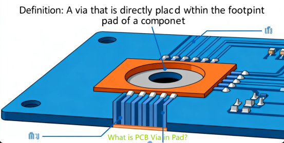
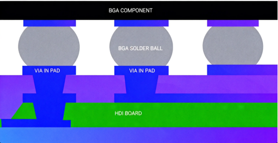
Let’s start with the basics: A “via” is the tiny hole in a PCB that connects copper traces across different layers. Traditional vias sit next to component pads (the small metal areas where chips or resistors are soldered).
Via in Pad (ViP) is exactly what it sounds like: The via is placed directly inside the component pad. Instead of having a gap between the via and the pad, the two merge into one structure.
But here’s the catch: You can’t just drill a hole in a pad and call it ViP. To work, the via must be filled and capped—usually with resin (conductive or non-conductive) and then plated with copper. In via-in-pad fabrication, both conductive fill (such as copper or conductive epoxy) and non conductive material (like epoxy or resin compounds) are used to fill the vias, depending on the design requirements. Advanced filling techniques, including copper filling and epoxy filling, help ensure reliable connections, prevent voids or cracks, and support high-density PCB designs. Why? Because an empty via in a pad would suck up solder during assembly, leaving the component poorly connected (a problem called “solder wicking”). Proper management of solder paste during assembly is also critical in via in pad designs to prevent manufacturing defects, ensure reliable electrical connections, and optimize thermal conductivity.
Why Use Via in Pad? 3 Key Benefits for High-Density Designs
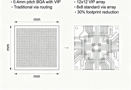
Traditional vias work for simple PCBs, but when your design gets tight (think: BGA chips with 0.4mm ball pitch), ViP becomes a game-changer. Here’s why it’s non-negotiable for modern electronics:
2.1 Space Savings
Via in pad technology allows for direct vertical connections, saving valuable board real estate. This enables more efficient component placement and maximizes pcb space, especially for small pitch components and fine pitch BGA packages.
2.2 Signal Integrity
Shorter signal paths through via in pad reduce signal loss and crosstalk. This approach also helps in minimizing parasitic inductance and achieving improved electrical performance, with pcb designers leveraging these benefits to meet demanding design requirements.
2.3 Thermal Management
Via in pad can be used to transfer heat away from high-power components by connecting thermal pads directly to internal copper planes. This enhances both thermal dissipation and heat management, supporting reliable operation in high-power designs.
Vias play a crucial role in enabling modern, high-density PCB designs by supporting increased component density, compact routing, and advanced package types.
A. Saves Critical Board Space
High-density PCBs (like those in smartphones or IoT sensors) have no room to waste. Traditional vias need extra space around the pad to avoid overlapping traces. With ViP, the via uses the pad’s existing area—freeing up space for more components or smaller board sizes.
For example: A BGA chip with 100 pins might need 20% less board space with ViP, because you don’t need to route traces around external vias.
B. Boosts Signal Integrity (No More Stub Problems)
Signal speed is everything in 5G, AI, or high-speed computing. Traditional vias leave a “stub”—a short section of unused copper inside the hole that reflects signals, causing delays or interference.
ViP eliminates stubs entirely: When the via is filled and capped, there’s no empty space for signal reflections. This makes ViP essential for designs handling signals above 10 GHz (like 5G base station PCBs).
C. Improves Thermal Management
Components like power amplifiers or processors generate heat. ViP acts as a “thermal bridge”: The filled via (especially conductive resin or copper-filled) transfers heat from the component pad to inner PCB layers, preventing overheating.
For example: A LED driver PCB using ViP can run 15–20°C cooler than one with traditional vias, extending component life.
Types of PCB Via in Pad: Conductive vs. Non-Conductive
Not all ViP is the same. The type you choose depends on your design’s needs—specifically, whether you need the via to conduct electricity or just save space.
A.Conductive Via in Pad
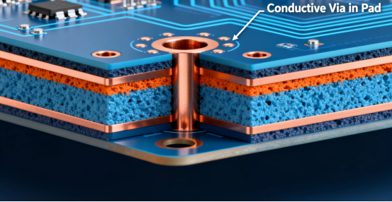
·How it works: The via is filled with conductive material (usually epoxy mixed with copper or silver particles) and plated with copper. This lets the via carry current through the pad—so the pad acts as both a solder point and a layer-to-layer connection.
·Best for: Power components (e.g., voltage regulators) or signal pins that need to connect to inner layers. For example, a BGA chip’s power pins often use conductive ViP to supply current directly from the top layer to the power plane below.
B.Non-Conductive Via in Pad
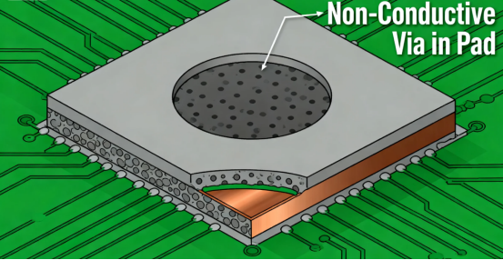
·How it works: The via is filled with non-conductive resin (no metal particles) and capped with copper. The via only provides structural support—no electrical connection.
·Best for: Signal pins that don’t need layer-to-layer connections (e.g., low-speed sensor pins). It’s cheaper than conductive ViP and works well for designs where signal integrity is key but current flow isn’t required.
PCB Design Considerations for Via in Pad
Designing a printed circuit board with via in pad technology opens up new possibilities for compact, high-performance electronic devices—but it also introduces unique challenges that require careful planning. To get the most out of via in pad, hardware engineers need to pay close attention to materials, layout, and the pcb fabrication process.
Material Selection Matters:Choosing the right solder mask and thermal pad materials is crucial. The solder mask should be precisely defined to prevent insufficient solder from seeping into the via during assembly, which can lead to weak solder joints or solder voids. For thermal pads, selecting materials that optimize heat dissipation is key—especially for power-hungry components. Non-conductive epoxy is often used to fill vias, preventing solder wicking and ensuring a flat, solderable surface. However, it’s important to match the epoxy’s coefficient of thermal expansion (CTE) with the PCB’s base material to avoid stress fractures during thermal cycling.
Selecting the Right Via Type:The choice between buried vias, blind vias, and through-hole vias will impact both the pcb fabrication process and the final board’s performance. Buried vias are ideal for connecting internal layers without affecting the board surface, making them popular in HDI PCB designs. Blind vias connect outer layers to internal layers, helping to maintain a compact pcb form factor. Through-hole vias, while more traditional, may not be suitable for fine pitch components or high-density layouts where via in pad technology truly shines.
Component Packages and Layout:When deciding whether to use via in pad, consider the component package type and size. Fine pitch components—like BGAs and other small pitch packages—often require via in pad to achieve the necessary component density and to escape component packages efficiently. For larger components or less dense layouts, traditional routing methods may suffice, and via in pad may not be necessary.
Optimizing Surface Routing and Signal Integrity:Using via in pad can greatly simplify routing on the board surface. By allowing you to drop vias directly into component pads, you can minimize trace length and reduce parasitic inductance, which is critical for maintaining signal integrity in high-speed designs. This approach also helps to enhance signal integrity by minimizing the number of vias and traces on the outer layers, reducing the risk of design rule check errors.
Annular Ring and Connection Reliability:The annular ring—the copper area surrounding the via—plays a vital role in ensuring reliable electrical connections and robust solder joints. The size of the annular ring should be carefully specified based on the pad size, via diameter, and your pcb manufacturer’s capabilities. A well-designed annular ring helps prevent issues like pad lifting and ensures a strong, consistent solderable surface.
Copper Filling and Thermal Management:Incorporating copper filling and thermal vias into your via in pad design can further improve both electrical performance and heat dissipation. Copper-filled vias provide a low-resistance path for electrical signals and help manage thermal expansion, while thermal vias in thermal pads offer a direct route for heat to escape from critical components to internal layers or heat sinks.
Common Mistakes to Avoid with Via in Pad
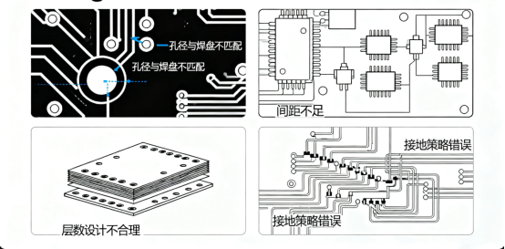
ViP is powerful, but it’s easy to mess up—especially if you skip key steps. One common pitfall is that via in pad introduces increased manufacturing complexity, which engineers and buyers should carefully consider. Here are the top 3 mistakes engineers and buyers make, and how to fix them:
Mistake 1: Forgetting to Fill the Via
An empty via in a pad is a disaster. During soldering, solder will flow into the hole (solder wicking), leaving the component with a weak joint. This causes intermittent connections or complete failure.
Fix: Always specify “filled and capped” ViP in your PCB specs. Ask your manufacturer for cross-sections of finished PCBs to confirm the via is fully filled (no bubbles or gaps).
Mistake 2: Using the Wrong Pad Size
If the pad is too small for the via, the via will take up most of the pad area—leaving no room for solder. This leads to cold joints (poor electrical contact). Using the wrong pad size can cause significant issues, especially in via-in-pad designs, where selecting appropriate pad sizes is crucial to meet manufacturing requirements, ensure proper via placement, and avoid problems with small BGA packages.
Fix: Follow IPC standards: The pad diameter should be at least 0.2mm larger than the via hole size. For example, a 0.3mm via needs a pad of at least 0.5mm.
Mistake 3: Ignoring Thermal Expansion
Resin and copper expand at different rates when heated. If the resin isn’t matched to the PCB’s thermal properties, it can crack over time—breaking the via or lifting the pad.
Fix: Choose a resin with a coefficient of thermal expansion (CTE) close to FR-4 (the most common PCB material). Your manufacturer can recommend resin types for your application (e.g., high-temperature resins for automotive PCBs).
When Should You Not Use Via in Pad?
ViP isn’t for every design. It adds cost and complexity, so save it for when you really need it. Here are 3 cases where traditional vias are better:
Low-density PCBs: If your board has plenty of space (e.g., a simple LED light PCB), traditional vias are cheaper and easier to manufacture.
Low-speed designs: If your signals are below 1 GHz (e.g., a basic Arduino shield), stub reflections won’t cause problems—so ViP is overkill.
Cost-sensitive projects: ViP adds 10–15% to PCB manufacturing costs (due to filling and capping steps). If your budget is tight, traditional vias are the way to go. Additionally, trace width constraints can make via in pad less suitable for designs with tight routing or small pitch components, as limited trace width may lead to design rule check errors and manufacturability issues.
How to Specify Via in Pad to Your PCB Manufacturer
To get high-quality ViP PCBs, you need to give your manufacturer clear specs. The via in pad process is a key technique in modern PCB manufacturing, improving space utilization and signal integrity for advanced electronic designs. Here’s what to include in your design file or quote request:
1.Via type: Conductive or non-conductive?
2.Hole size: E.g., 0.2mm, 0.3mm (match to your component’s pad size).
3.Filling material: For conductive ViP—specify resin type (e.g., copper-filled epoxy); for non-conductive—ask for high-temperature resin (if needed).
4.Capping requirement: Must the filled via be plated with copper (to match the pad’s finish)?
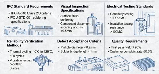
5.Inspection standards: Request IPC-A-600 Class 2 or 3 (Class 3 for aerospace/medical devices) to ensure no voids or pad lifting.
6.Microvia creation: For high-density via in pad designs, specify if laser drilling is required to create small, precise microvias.
Final Thoughts: Is Via in Pad Right for Your Design?
If you’re working on a high-density, high-speed, or thermally demanding PCB—yes, ViP is worth the investment. It solves the space and signal problems that traditional vias can’t, and it’s becoming standard for modern electronics like 5G devices, AI chips, and medical equipment.
The key is to work with a PCB manufacturer experienced in ViP (ask for their ViP project portfolio!) and clearly specify your requirements. With the right approach, ViP will make your design more reliable, smaller, and faster—without unnecessary headaches.
Do you have a specific ViP project in mind? Let us know in the comments, and we can help you troubleshoot or find the right manufacturing partner!
FAQs
Q. What is PCB Via in Pad?
A. It refers to a PCB layout technique where a via is placed directly within a component pad. This requires specialized processes such as resin filling and metal capping to prevent solder loss or signal interference, making it a core solution for high-density interconnect (HDI) designs.
Q. What is the core difference between Via in Pad and a standard via?
A. Standard vias are placed outside the pad, requiring spacing to avoid interference. Via in Pad merges with the pad to save routing space but must be filled/capped — otherwise, solder can flow into the hole, causing poor connections. This is the most critical distinction.
Q. What are the common types of Via in Pad?
A. Two functional categories exist:
·Conductive type: Filled with copper/silver-containing conductive resin, enabling both pad connection and interlayer conductivity — ideal for power pins.
·Non-conductive type: Filled with insulating resin, serving only for space optimization — often used for signal pins.
Q. What are the dimensional guidelines for designing Via in Pad?
A. Follow the principle of "smaller hole diameter requires proportional outer diameter matching": Typically, the inner diameter should be ≥0.1mm (4mil), and the pad outer diameter should be at least 0.2mm (8mil) larger than the hole diameter. For example, a 0.3mm hole requires a 0.5mm or larger pad to prevent drill offset from damaging the pad.
Q. Must Via in Pad be filled? What issues arise if left unfilled?
A. Yes, filling is mandatory. Unfilled Via in Pad can cause "solder wicking" during soldering, leading to poor solder joints or tombstoning. Additionally, trapped gas expanding during reflow can generate solder beads, potentially causing short circuits.
Q. How to correctly configure Via in Pad in design software?
A. In Altium Designer, for example, check the "Fill + Cap" option in the Via properties. When generating Gerber files, ensure the solder mask layer covers the filled via positions to avoid unintended openings.
Q. In which scenarios is Via in Pad essential, and when is it not recommended?
A. Essential for: BGA chips with pin pitches below 0.4mm, 5G high-frequency modules, ultra-thin laptops, and other high-density/high-speed designs where it reduces trace length and improves signal integrity.
Not recommended for: Low-density/low-speed products like simple LED boards or basic control boards, as it increases manufacturing costs by 10-15% without performance benefits.
Q. Are there specific surface finish requirements for Via in Pad?
A. No special restrictions; it is compatible with common finishes like ENIG (Electroless Nickel Immersion Gold) and HASL. However, ensure the filled via surface is flush with the pad to avoid uneven plating affecting solderability.
Q. Can blind or buried vias be used as Via in Pad?
A. Yes, and this is common in HDI designs. Using a 1st-order blind via (e.g., surface to L2) as Via in Pad offers cost-effective space savings. However, higher-order blind vias (e.g., L2 to L5) can cause exponential cost increases and should be used cautiously.
Q. What are the core quality inspection standards for Via in Pad?
A. Three key criteria:
·No voids/bubbles in the fill
·Strong adhesion between the resin and plated copper wall
·A flat surface without protrusions that could affect component placement. Typically, compliance with IPC-A-600 Class 2 or 3 is required.
Q. How much does Via in Pad increase costs?
A. It adds 10-20% compared to standard vias, mainly due to extra steps like resin filling, precision drilling, and secondary plating. For high-end products, however, this avoids performance issues caused by congested routing, proving more cost-effective long-term.
Q. How to mitigate soldering risks with Via in Pad during assembly?
A. Prioritize placing components with Via in Pad on the secondary reflow side to avoid solder bumps affecting stencil contact on the opposite side. Additionally, design "wetting zones" (exposed copper areas) opposite the vias to guide excess solder distribution and minimize solder bead formation.
Author: Jack Wang

