


Troubleshooting PCB Via Filling: Common Problems and Solutions
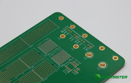
PCB via filling, a critical process in printed circuit board (PCB) manufacturing, plays a vital role in ensuring the quality and reliability of electronic devices. It involves filling the holes (vias) within the PCB with specific materials like resin or ink, which were originally intended for electrical connections between layers. This step helps prevent issues like short circuits, corrosion, and signal interference—problems that can arise from unfilled vias during the assembly process.
This article covers the key aspects of PCB via filling, focusing on its importance, common methods, and the challenges faced during production. We’ll explore the main goals of via filling, including how it supports high-density interconnect designs and improves PCB reliability. The article also addresses common issues, such as air bubbles, ink shrinkage, and incomplete filling, offering practical solutions. By understanding these processes and challenges, manufacturers can optimize their production lines and create more reliable, high-performance PCBs.
Whether you're a seasoned PCB designer or just starting out, understanding the importance of via filling is essential for producing high-quality, reliable electronic products.
What is PCB Via Filling?
PCB via filling is a manufacturing process in PCBs where specific holes (vias) are filled with a material like resin, ink, or conductive adhesives. These holes are typically used to connect different layers of a multi-layer PCB. However, in certain situations, these vias must be filled and sealed to prevent issues like solder bridging, corrosion, or interference with the PCB’s electrical performance.
Vias can be created for various reasons, such as routing electrical signals between layers or cooling components. PCB via filling helps improve the quality, reliability, and functionality of the circuit board by filling these holes with materials that prevent issues caused by moisture, chemical residues, or electrical short circuits. This process is essential in advanced PCB designs, especially for high-density interconnect (HDI) boards and surface-mount technology (SMT) applications.
Main Purposes and Application Scenarios
Preventing SMT Solder Short Circuits
The primary purpose of via filling is to prevent solder from flowing through the vias during the soldering process, especially when working with surface-mount technology (SMT). For instance, in BGA (Ball Grid Array) soldering, the solder paste can seep through the vias, causing short circuits or poor connections. Filling the vias with resin or ink before the soldering process ensures that no solder flows through the vias, preventing these issues and improving the quality of the final assembly.
Real-life Example: In high-density PCBs, especially those used in smartphones or computer processors, via filling ensures that the small vias under BGA pads do not interfere with soldering, making the board more reliable.
Avoiding Chemical Residues
During the manufacturing and cleaning of PCBs, chemicals like flux or cleaning agents can remain trapped in the vias if they are not filled. This leftover chemical residue can lead to corrosion or failure of the PCB over time. Via filling helps to seal these holes, preventing the trapped chemicals from escaping and causing issues such as corrosion, ion migration, or electrical faults.
Real-life Example: In aerospace and automotive electronics, where PCBs are exposed to harsh environments, sealing vias can prevent long-term damage from chemicals and moisture.
Supporting High-Density Interconnect (HDI) Designs
In advanced PCB designs like HDI boards, vias are often placed directly under pads in a design known as Via-in-Pad. These vias must be filled and plated over to ensure proper electrical connections and a flat surface for component mounting. This process ensures that vias do not interfere with the delicate high-speed connections, as seen in microelectronics and high-performance computing.
Real-life Example: In mobile phones, where space is limited, HDI PCBs with filled vias allow manufacturers to place more components in a smaller area, boosting the device’s performance and capabilities.
Enhancing PCB Reliability
Via filling also improves the mechanical reliability of the PCB by preventing the buildup of moisture or air inside the vias. This is especially important in extreme temperature or high-humidity environments where trapped moisture can lead to damage or failure due to thermal expansion. Filling vias with materials like resin can reduce the risk of these issues, enhancing the overall durability of the PCB.
Real-life Example: Industrial-grade electronics often use filled vias to ensure that the board maintains its performance in harsh environments, such as extreme temperatures or high humidity.
Improving Lamination Flatness
During the lamination process, if large vias are left unfilled, they can cause uneven surfaces, leading to issues with the copper layers and signal integrity. Via filling helps create a smoother surface by filling in these holes, ensuring better alignment and adhesion of the layers. This improves the board’s overall mechanical strength and functionality.
Real-life Example: In multi-layer PCBs used in consumer electronics, via filling ensures that the layers bond together seamlessly, preventing issues like delamination and improving the electrical performance.
What Are the Main Purposes of PCB Via Filling?
The main purposes of PCB via filling are to prevent solder short circuits, avoid chemical residue buildup, support high-density interconnect designs, enhance reliability, and improve lamination flatness.
1. Preventing SMT Solder Short Circuits
PCB via filling prevents solder from flowing through vias during the soldering process, particularly in SMT applications, where solder can cause shorts or poor connections.
In SMT (Surface-Mount Technology) assembly, vias are small holes that connect different layers of a PCB. If these vias are left unfilled, molten solder during the reflow soldering process can flow through the vias, causing solder bridges or shorts between different traces or pads. This is especially problematic with BGA (Ball Grid Array) components, where the solder pads are close to vias. Filling these vias before the soldering process ensures that no solder can escape into these holes, maintaining the integrity of the PCB and preventing short circuits.
Real-life Example: In high-performance electronics like smartphones or laptops, where many small components are packed together, via filling ensures that solder does not flow through vias under BGA pads, thus preventing short circuits and improving device reliability.
2. Avoiding Chemical Residue
Via filling prevents chemical residues like flux or cleaning agents from remaining in vias, which could lead to corrosion or electrical failure.
During PCB manufacturing, chemicals like flux and cleaning agents are used for soldering and cleaning. If these chemicals remain in unfilled vias, they can eventually cause corrosion or migration of ions that can disrupt the electrical performance of the PCB. Via filling seals these holes, preventing any chemical residue from remaining trapped and ensuring the long-term stability and reliability of the PCB.
Real-life Example: In industries like automotive or aerospace, where PCBs are exposed to harsh conditions, via filling helps protect against chemical damage and maintains the board’s performance over time.
3. Supporting High-Density Interconnect (HDI) Designs
Via filling supports complex designs like Via-in-Pad (VIP) in HDI boards, where filled vias are essential for efficient signal routing and component mounting.
High-Density Interconnect (HDI) PCBs are used in advanced applications where space is limited and signal integrity is critical, such as in smartphones or advanced computing devices. In HDI designs, vias may be placed directly under the pads (known as Via-in-Pad). To create a flat, solderable surface, these vias need to be filled and plated. Via filling ensures that the surface remains smooth, preventing issues with mounting components and allowing for precise signal routing in compact designs.
Real-life Example: In mobile phone PCBs, Via-in-Pad designs are common to save space. Via filling allows for efficient component placement and stable electrical connections.
4. Enhancing PCB Reliability
Via filling enhances the mechanical and electrical reliability of a PCB by reducing the risks of thermal stress and preventing damage to the via walls.
During PCB operation, especially in environments with fluctuating temperatures, thermal expansion and contraction can lead to cracks or damage in unfilled vias. Via filling, particularly with materials like resin, helps to absorb thermal stresses and prevent the vias from cracking. This results in a more durable PCB, capable of withstanding harsh environments without compromising its mechanical or electrical performance.
Real-life Example: In industrial-grade electronics, where equipment must endure extreme temperature fluctuations, filled vias provide enhanced durability, preventing failure due to heat-related stresses.
5. Improving Lamination Flatness
Via filling ensures a flat surface for the lamination process, improving the overall quality and signal integrity of multi-layer PCBs.
During the lamination of multi-layer PCBs, unfilled vias can create uneven surfaces, which can lead to problems with the adhesion of the copper layers and cause signal integrity issues. By filling the vias before lamination, the surface becomes smoother, ensuring that all layers bond properly and maintain their structural integrity. This also helps improve alignment during assembly and reduces the risk of layer delamination, enhancing the overall quality of the PCB.
Real-life Example: In high-performance circuit boards, such as those used in automotive or medical devices, via filling ensures that multi-layer PCBs are properly aligned during lamination, improving performance and reducing the risk of defects.
What Are the Common Types of PCB Via Filling?
The common types of PCB via filling are resin via filling, ink via filling, and conductive adhesive via filling, each suited for different applications based on performance, cost, and electrical requirements.
1. Resin Via Filling
Resin via filling uses specialized resin materials to fill the vias, offering excellent filling properties, low shrinkage, and stable electrical performance.
Resin via filling is the most commonly used method for filling vias in high-performance PCBs. The primary advantage of resin is its ability to completely fill vias with a smooth surface and minimal shrinkage. Once cured, resin creates a strong, durable bond with the PCB, ensuring the via remains stable even in demanding environments. The electrical properties of resin are also reliable, making it suitable for high-frequency and high-speed applications.
Applications: Resin via filling is commonly used in HDI boards, where the vias are often smaller and placed under BGA pads. These boards require filled vias to maintain a smooth surface for component mounting and to avoid soldering issues. It is also crucial in BGA soldering, where the vias must be filled to prevent solder from leaking through and causing short circuits.
Real-life Example: In mobile phones, where space is limited and high performance is required, HDI boards often use resin-filled vias to ensure reliable and precise component connections.
2. Ink Via Filling
Ink via filling is a cost-effective and simple process that uses solder mask ink to fill the vias, but it has limited filling depth and is not suitable for all applications.
Ink via filling involves using a type of solder mask ink that fills the vias in a PCB. While it is a more affordable solution, it has limitations in terms of how deep it can fill the vias and its ability to maintain a perfectly smooth surface. The ink does not have the electrical conductivity properties of resin, so it is typically used for non-critical vias where electrical performance is not a major concern.
Applications: Ink via filling is primarily used for non-pad vias that are not in contact with solder pads, such as those used in preventing flux from entering vias during the soldering process. It is ideal for vias that do not need to be electrically conductive and are not part of high-density designs.
Real-life Example: In consumer electronics, where the cost of manufacturing is a major factor, ink-filled vias are used to prevent flux residues from contaminating vias without needing the high performance of resin-filled vias.
3. Conductive Adhesive Via Filling
Conductive adhesive via filling uses conductive materials like silver or copper to fill vias, providing electrical connection between layers and replacing plated holes in some applications.
Conductive adhesive via filling involves using a material that contains metal particles, such as silver or copper, to fill the vias. The key advantage of this method is that it creates an electrical connection between different layers of the PCB, which can replace traditional electroplated vias. This makes it particularly useful in designs where a conductive path is needed through the via, without requiring the full copper plating process.
Applications: Conductive adhesive via filling is most commonly used in specialized HDI boards and flexible PCBs. These applications often require conductive vias to achieve certain structural or electrical goals, such as connecting layers in a flexible design or providing high-speed electrical connections. Conductive adhesives are especially useful in designs where traditional copper plating may be impractical.
Real-life Example: In flexible printed circuit boards (FPCBs) used in wearables, conductive adhesive via filling ensures that electrical connections are maintained even as the board bends and flexes.
Comparison Table: Resin, Ink, and Conductive Adhesive Via Filling
Type Features Applications Advantages Limitations Resin Via Filling Excellent filling ability, low shrinkage, stable electrical properties HDI boards, BGA pads, high-performance PCBs Strong, durable, stable electrical performance Higher cost compared to ink filling Ink Via Filling Simple, cost-effective, limited filling depth, not suitable for high electrical performance Non-pad vias, flux prevention in low-performance areas Affordable, quick process Limited depth, non-conductive, less durable Conductive Adhesive Electrically conductive, replaces electroplated vias, uses metal particles like silver or copper HDI boards, flexible PCBs, high-speed circuits Creates electrical connections between layers More expensive, not as common as resin or ink
| Type | Features | Applications | Advantages | Limitations |
| Resin Via Filling | Excellent filling ability, low shrinkage, stable electrical properties | HDI boards, BGA pads, high-performance PCBs | Strong, durable, stable electrical performance | Higher cost compared to ink filling |
| Ink Via Filling | Simple, cost-effective, limited filling depth, not suitable for high electrical performance | Non-pad vias, flux prevention in low-performance areas | Affordable, quick process | Limited depth, non-conductive, less durable |
| Conductive Adhesive | Electrically conductive, replaces electroplated vias, uses metal particles like silver or copper | HDI boards, flexible PCBs, high-speed circuits | Creates electrical connections between layers | More expensive, not as common as resin or ink |
What is the PCB Via Filling Process?
The PCB via filling process involves cleaning and drying the vias, applying ink or resin to fill them, curing the material, and ensuring the vias are properly sealed to prevent contamination and improve the board’s performance.
1. Pre-treatment
Pre-treatment involves cleaning and preparing the vias to ensure proper adhesion of the filling material and prevent issues like oil bubbling during the curing process.
Before filling the vias, it is crucial to clean the holes to remove any dirt, debris, or residues that might affect the filling process. This step typically involves chemical cleaning or mild etching, followed by mechanical brushing to ensure the holes are free from contaminants. Additionally, the PCB must be thoroughly dried to remove any moisture inside the vias. If any moisture is left, it can turn into steam during the curing process, causing "oil bubbling" or defects in the final product. Ensuring a clean and dry surface is critical for the success of the subsequent filling steps.
Real-life Example: In high-precision electronics like medical devices or aerospace components, ensuring clean and dry vias is essential to prevent moisture-related issues during the soldering process.
2. Ink Via Filling
Ink via filling uses a screen printing method to apply solder mask ink into the vias, ensuring they are completely filled with the help of vacuum suction.
In this step, a specialized screen printing technique is used to apply solder mask ink into the vias. The PCB is aligned with a screen mesh that matches the via locations. The ink is spread over the mesh using a squeegee, filling the vias. After applying the ink, vacuum suction is applied from the bottom of the PCB to help draw the ink deep into the vias and remove any trapped air, ensuring complete filling. This process is crucial for preventing flux from entering vias during soldering and avoiding contamination.
Real-life Example: Ink via filling is commonly used in consumer electronics like televisions or gaming consoles, where preventing flux contamination is important without requiring high-performance via filling.
3. Pre-baking
Pre-baking is done to dry the surface of the ink, ensuring that it doesn't get washed away during the next steps of the process.
After ink is applied to the vias, pre-baking (also known as pre-curing) is necessary to dry the surface of the ink and give it a "dry-to-the-touch" state. This step helps to prevent the ink from being washed away or disturbed during the following steps, such as the surface ink printing or exposure process. Pre-baking typically involves heating the PCB at a controlled temperature (usually around 75°C) for a set time (often around 30–40 minutes). Proper temperature and time control are essential; insufficient baking may result in incomplete curing, while overbaking can lead to surface hardening without fully curing the ink inside the vias.
Real-life Example: In mass-produced PCBs for everyday electronics, such as smartphones, pre-baking ensures that the ink remains intact throughout the production process, minimizing defects in the final product.
4. Surface Ink Printing
Surface ink printing involves applying a solder mask layer to the surface of the PCB using screen printing or spraying methods.
In this step, a solder mask is applied to the surface of the PCB to provide insulation and prevent unwanted solder bridges. This layer is typically printed using screen printing or spraying methods, depending on the specific design requirements. The purpose of the surface ink is to protect the PCB from environmental factors, improve the overall quality of the board, and ensure that the vias are sealed and non-conductive. The ink must be applied evenly to cover all exposed copper traces and pads.
Real-life Example: In circuit boards used for computer processors, the surface ink prevents corrosion, ensures electrical isolation, and ensures smooth performance by keeping unwanted elements off the copper traces.
5. Exposure and Development
Exposure uses UV light to harden the solder mask ink, and development removes unwanted ink from the exposed areas, leaving a clean pattern.
The exposure process uses ultraviolet (UV) light to cure the solder mask ink in the areas where it is needed. A photomask is placed over the PCB, and UV light is used to harden the ink in the desired areas. After exposure, the PCB undergoes a development process where a solution (typically sodium carbonate) is used to wash away the unexposed ink. This creates the final pattern on the PCB, leaving only the desired ink in place, and ensuring clean via and pad areas.
Real-life Example: In the production of HDI boards for high-end electronics, such as mobile phones, exposure and development ensure that the vias are properly isolated and only the necessary areas remain covered by the solder mask.
6. Post-curing
Post-curing solidifies the solder mask ink completely, ensuring strong adhesion and durability, and is crucial for long-term performance.
After the exposure and development steps, post-curing is performed to fully cure the solder mask and ensure it has achieved its final properties. The PCB is baked at a higher temperature (usually around 150°C) for a specified duration (typically 30–60 minutes). This step is crucial for ensuring that the ink has fully cross-linked, increasing its strength, durability, and electrical insulation properties. Proper curing also ensures that the solder mask adheres firmly to the PCB, providing long-term protection against environmental damage.
Real-life Example: In automotive or industrial-grade electronics, where PCBs are subjected to harsh environments, post-curing ensures that the solder mask remains intact and provides reliable protection.
Common Issues in the PCB Via Filling Process and Their Solutions
Common issues in the PCB via filling process include bubbles, excessive ink shrinkage, hole damage, ink overflow, and incomplete filling, with solutions such as adjusting ink viscosity, optimizing pre-baking and vacuum systems, and cleaning the screen mesh.
1. Bubbles/Holes
Bubbles or holes occur when the ink has high viscosity or when the vacuum system is insufficient, leading to trapped air or incomplete filling.
When the ink used in the via filling process has too high a viscosity (thickness), it does not flow easily into the vias, trapping air and causing bubbles or holes in the filled vias. Additionally, an insufficient vacuum system may fail to fully remove air from the vias, leading to the same issue. This can result in weak spots in the PCB and negatively affect its performance.
Solution: To solve this, you can adjust the ink viscosity to ensure it flows smoothly and evenly into the vias. Using a lower-viscosity ink or adding a thinner can help. Additionally, optimizing the vacuum system ensures that all air is properly evacuated from the vias during the filling process, preventing the formation of bubbles or holes.
Real-life Example: In consumer electronics, where PCBs must perform reliably for long periods, bubbles or holes in vias can cause electrical failures, so ensuring a proper vacuum system is critical.
2. Excessive Ink Shrinkage
Excessive ink shrinkage can occur due to high shrinkage rates of the ink or insufficient pre-baking or curing, causing dips or uneven surfaces in the filled vias.
When the ink used for via filling has a high shrinkage rate, it may pull away from the walls of the via during the curing process, creating large dips or uneven surfaces. If the pre-baking or curing times are insufficient, the ink may not fully solidify, leading to further shrinkage during the final curing phase.
Solution: The solution to this issue is to select ink with a lower shrinkage rate, which will maintain a more consistent surface during curing. Additionally, optimizing the curing process by adjusting the temperature and time can help ensure the ink fully solidifies, reducing the chances of shrinkage.
Real-life Example: In high-end PCB manufacturing for products like medical devices, where precision is critical, using low-shrinkage ink ensures the vias remain smooth and functional.
3. Hole Damage After Development
Hole damage can occur if the pre-baking process was insufficient or if the development pressure is too high, causing the ink in the vias to be washed away.
After the exposure step, the PCB is developed to remove unwanted ink. If the pre-baking process was not thorough, the ink inside the vias may not be fully hardened, and the pressure from the development process can wash it away, leading to damaged or incomplete vias. High development pressure or excessive time can also exacerbate this issue.
Solution: To avoid this, increase the pre-baking time and temperature to ensure the ink is sufficiently hardened. Additionally, adjusting the development parameters, such as reducing pressure or development time, can prevent the vias from being damaged.
Real-life Example: In the production of flexible PCBs used in wearables, maintaining the integrity of the vias is crucial to avoid failure due to washed-out ink during the development process.
4. Ink Overflow/Excessive Ink on the Surface
Ink overflow or excessive ink on the surface of the PCB happens when moisture is trapped inside the vias or when pre-baking is insufficient, causing the ink to bubble during curing.
If moisture remains trapped inside the vias, it can vaporize during the curing process, causing the ink to bubble and overflow, resulting in visible ink protrusions or “oil explosion.” Insufficient pre-baking can also leave some solvent inside the ink, which leads to bubbling when the curing process begins.
Solution: To prevent this, strengthen the cleaning and drying process to ensure all moisture is removed from the vias before filling. Additionally, ensure thorough pre-baking to remove any residual solvents in the ink, which could cause bubbles during curing.
Real-life Example: In automotive PCBs, where the PCB is exposed to extreme environmental conditions, moisture inside vias can cause bubbling during the curing process, leading to performance issues. Proper cleaning and pre-baking can prevent this.
5. Incomplete Filling of Vias
Incomplete via filling may occur due to clogged screen mesh openings or poor ink flow, resulting in vias that are not fully filled.
If the screen mesh used during ink via filling is clogged or if the ink does not flow smoothly, the vias may not be completely filled, leaving gaps or voids. This can lead to unreliable electrical connections or weak points in the PCB.
Solution: Regularly clean the screen mesh to prevent clogging and ensure smooth ink flow. Additionally, adjust the ink viscosity to make sure it flows properly and fills the vias completely. If needed, use a different ink type to improve flow characteristics.
Real-life Example: In high-precision PCBs for communications equipment, incomplete filling of vias can cause signal integrity issues. Regular maintenance of equipment and adjusting ink flow ensures consistent results.
How to Improve PCB Via Filling Yield and Reliability
Improving PCB via filling yield and reliability involves optimizing the process workflow, strictly controlling temperature and time, and selecting high-quality equipment and materials.
1. Optimize the Process Workflow
Streamlining the process workflow improves efficiency and reduces the chances of defects, ensuring higher yield and reliability in PCB via filling.
Optimizing the entire via filling process is crucial for improving both yield and reliability. This involves ensuring each step, from pre-treatment to post-curing, is performed correctly and consistently. A well-organized workflow minimizes errors and reduces the potential for common issues, such as air bubbles, incomplete filling, and improper curing. By automating certain steps and reducing manual handling, the risk of human error is minimized, improving the overall quality of the PCBs.
For example, ensuring proper alignment during ink application and consistent vacuum pressure during the filling stage can prevent issues like bubbles or voids. Using quality control checks at each step, such as inspecting pre-treatment cleanliness and verifying curing times, can also help spot problems early, preventing defects from affecting the final product.
Real-life Example: In high-performance electronic products like smartphones, an optimized workflow ensures that the tiny vias are filled properly, minimizing defects and improving the board’s overall functionality.
2. Strictly Control Temperature and Time
Proper control of temperature and time during each step, especially pre-baking and curing, is essential for achieving consistent and reliable via filling.
Temperature and time play a significant role in the PCB via filling process, particularly during pre-baking and curing stages. If the temperature is too high or too low, or if the curing time is too short or too long, it can lead to issues such as excessive ink shrinkage, improper curing, or incomplete filling. For example, inadequate pre-baking can cause residual moisture in the vias, which may lead to bubbles during the curing process.
By strictly controlling these factors, manufacturers can ensure the ink or resin used for filling is properly cured, reducing the risk of defects such as shrinking or cracking. Following the manufacturer’s recommended guidelines for each material used is critical to avoid over-curing or under-curing, both of which can affect the reliability and performance of the final product.
Real-life Example: In high-precision industries, such as aerospace, where reliability is paramount, controlling temperature and time is essential to ensure the PCB vias maintain their strength and functionality in extreme conditions.
3. Improve Equipment and Material Selection
Brief Answer: Using high-quality equipment and materials designed for specific PCB via filling requirements ensures better fill quality and enhances the reliability of the final product.
The choice of equipment and materials is critical in improving PCB via filling reliability and yield. High-quality equipment ensures precision in ink application, vacuum suction, and curing. For example, using automated screen printing machines with consistent pressure can prevent issues like clogged mesh or uneven ink distribution. Additionally, optimizing the vacuum system ensures that air is effectively removed from the vias, preventing bubble formation.
Selecting the right materials, such as low-shrinkage inks or high-quality resins, also plays a significant role in the outcome of the via filling process. Low-shrinkage inks, for example, reduce the risk of dips or uneven surfaces, while resins with stable electrical properties are essential for high-performance PCBs.
Real-life Example: In consumer electronics, the use of high-quality inks and automated equipment in the PCB manufacturing process ensures that each via is filled perfectly, enhancing the performance and longevity of devices like tablets and laptops.
Conclusion
PCB via filling is a critical process in modern PCB manufacturing, ensuring reliable electrical connections, preventing defects, and supporting the overall integrity of electronic products. As the demand for smaller, faster, and more efficient devices continues to rise, the importance of precise via filling will only grow, making it essential for manufacturers to focus on optimizing workflows, selecting quality materials, and implementing advanced technologies. Looking ahead, the future of PCB via filling will likely see even more innovative solutions, such as the use of advanced resins, automation, and AI-driven quality control systems, to enhance both yield and reliability.
At PCBMASTER, we understand the challenges and requirements of high-quality PCB and PCBA production. With years of experience in the industry, we are committed to delivering top-notch products and services, ensuring that our clients receive the most reliable and efficient solutions for their needs. Whether for complex designs or high-performance applications, PCBMASTER is your trusted partner in the world of PCB manufacturing.
FAQs
What materials are needed for PCB via filling?
There are several materials commonly used for PCB via filling, including resin, ink, and conductive adhesive.
l Resin filling materials, such as epoxy or specialized tree resins, are ideal for providing excellent adhesion and mechanical strength.
l Ink filling materials, typically solder mask ink, are used for less critical applications and are cost-effective.
l Conductive adhesives are used in specific designs where electrical continuity is necessary through the via, like in certain high-density interconnect (HDI) boards.
Each material serves a unique purpose based on the required performance. Resin is preferred for high-performance applications requiring high durability, while ink is used for non-critical vias to prevent solder contamination and chemical residues. Conductive adhesives are used in cases where electrical connections through the vias are necessary.
How to avoid bubble issues in ink-filled vias?
Bubbles in the via filling process can occur due to several factors, such as high ink viscosity, insufficient vacuum pressure, or residual moisture in the vias. The most common cause is that the ink is too thick, trapping air inside the vias. This can be resolved by adjusting the ink viscosity, ensuring it flows smoothly and fills the via completely. Another solution is to optimize the vacuum system used during filling to ensure all air is evacuated from the vias. Additionally, pre-treating the PCB to ensure there is no moisture left in the vias before filling is critical for preventing bubble formation.
When should resin filling be used instead of ink filling?
Resin filling is preferred over ink filling in situations where higher durability, structural integrity, and electrical performance are required. The main difference between resin and ink filling is that resin, particularly epoxy-based, offers better mechanical strength and adhesion, making it ideal for high-performance applications such as HDI (High-Density Interconnect) boards and BGAs (Ball Grid Arrays). Resin filling is also used when the vias need to be plated with copper, as the resin material is compatible with electroplating. On the other hand, ink filling is typically used for less demanding applications where the primary goal is to prevent solder contamination or chemical penetration.
How to control curing time and temperature for ink via filling?
Curing time and temperature are crucial factors that influence the final quality of ink-filled vias. If the curing process is too short or the temperature is too low, the ink may not fully harden, leading to incomplete filling or a soft surface that could degrade under stress. Conversely, excessive curing temperature or time could cause the ink to shrink or crack, leading to weak or defective vias. To avoid over- or under-curing, it is important to follow the manufacturer's recommended curing temperature and time closely, typically around 150°C for 60 minutes for most inks. The ideal approach involves carefully controlling both temperature and time, ensuring consistent and complete curing of the ink.
Can via filling improve the overall durability of the PCB product?
Yes, via filling significantly enhances the durability of the PCB by preventing moisture, air, and contaminants from entering the vias, which could cause corrosion, short circuits, or signal degradation. The filling material adds structural integrity to the PCB, reducing the risk of mechanical failure during thermal cycling and mechanical stress. To ensure the via filling process contributes positively to the PCB’s long-term reliability, it is crucial to maintain strict quality control throughout the process. This includes ensuring the filling material is properly cured, the vias are fully filled, and there are no bubbles or gaps in the filling, which would compromise the performance of the PCB over time.
Author Bio
Hi, I'm Carol, the Overseas Marketing Manager at PCBMASTER, where I focus on expanding international markets and researching PCB and PCBA solutions. Since 2020, I've been deeply involved in helping our company collaborate with global clients, addressing their technical and production needs in the PCB and PCBA sectors. Over these years, I've gained extensive experience and developed a deeper understanding of industry trends, challenges, and technological innovations.
Outside of work, I'm passionate about writing and enjoy sharing industry insights, market developments, and practical tips through my blog. I hope my posts can help you better understand the PCB and PCBA industries and maybe even offer some valuable takeaways. Of course, if you have any thoughts or questions, feel free to leave a comment below—I'd love to hear from you and discuss further!

