


PCB Design Essentials: Understanding the Impact of Hole Copper Thickness
The copper thickness around PCB holes is a critical factor that often goes unnoticed in the design process. Despite its small scale, it directly impacts electrical conductivity, mechanical strength, and thermal performance. Whether designing for high-frequency applications or power-intensive circuits, the right hole copper thickness ensures reliable connections and long-term durability. Let’s explore why this essential design element should never be overlooked.
What is Hole Copper Thickness in PCB Design and Why Does It Matter?
Hole copper thickness in PCB design refers to the layer of copper applied to the inner walls of vias, which is crucial for ensuring reliable electrical connections, mechanical strength, heat dissipation, and signal integrity in the final circuit board.
Definition of Hole Copper Thickness: How Copper is Applied to Holes in PCBs Through Processes Like Electroplating
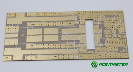
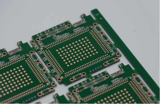
Hole copper thickness refers to the layer of copper applied to the walls of holes in a printed circuit board (PCB). These holes, also known as vias, are drilled through the PCB to allow electrical connections between different layers of the board. Copper is applied to the inner surface of these holes through a process called electroplating. In electroplating, a thin layer of copper is deposited onto the hole's walls by passing an electrical current through a copper solution. This creates a conductive path that connects different circuit layers, ensuring the board's electrical connections are complete and reliable. The thickness of this copper layer can vary depending on the design requirements and the specific application, influencing the PCB's overall performance.
Copper Thickness’s Impact on Electrical Conductivity: How Thickness Affects Current Flow, Resistance, and Power Loss
The copper thickness in a PCB hole directly affects the flow of electricity. Thicker copper improves the electrical conductivity of the via, which means less resistance to current flow. Lower resistance leads to reduced power loss and improved efficiency. For instance, in power-intensive applications, such as power supplies or high-current circuits, a thicker copper layer ensures that enough current can flow through without excessive heat buildup or voltage drop. Conversely, thin copper layers can result in higher resistance, leading to inefficiency and overheating, which may ultimately damage the PCB. Therefore, selecting the correct copper thickness is critical for ensuring the PCB performs as expected, particularly in high-power or high-frequency environments.
Mechanical Strength: How Thicker Copper Increases Structural Integrity and Durability
Copper thickness is not just about electrical performance; it also plays a role in the mechanical strength of the PCB. A thicker copper layer inside the hole improves the structural integrity of the via, making it more resistant to mechanical stress, such as vibrations or thermal expansion. This is particularly important in applications where the PCB is subjected to harsh environments or frequent movement, such as automotive or industrial electronics. Thicker copper reduces the likelihood of via failure or cracking, ensuring that the PCB remains durable over time. In contrast, a thinner copper layer may not be able to withstand mechanical forces as well, potentially leading to cracks, delamination, or even complete failure of the PCB in extreme conditions.
Thermal Management: The Role of Hole Copper in Heat Dissipation for Preventing Thermal Failure
Another critical aspect of hole copper thickness is its impact on thermal management. PCBs, especially in high-power applications, generate heat as current flows through the circuits. Thicker copper in the vias helps to dissipate heat more effectively, preventing the board from overheating. Heat dissipation is crucial to avoid thermal failure, which can degrade the performance of the PCB or cause complete system failure. For example, in power electronics like voltage regulators or RF amplifiers, copper thickness is chosen carefully to ensure the PCB can handle the heat produced during operation. If the copper layer is too thin, the heat may not spread efficiently, causing localized hotspots that can damage sensitive components. Adequate copper thickness ensures that heat is spread evenly across the PCB, maintaining performance and prolonging its lifespan.
Signal Integrity in High-Frequency Designs: Copper Thickness as a Factor in Reducing Signal Distortion at High Frequencies (e.g., in RF Circuits)
In high-frequency applications, such as RF (Radio Frequency) circuits, copper thickness in the vias plays a crucial role in maintaining signal integrity. At high frequencies, signal distortion, or attenuation, can occur if the via’s copper layer is too thin. Thicker copper reduces the inductive and resistive losses in the vias, ensuring that signals travel more efficiently with minimal interference. This is especially important in applications where signal fidelity is critical, like in 5G networks, GPS systems, or high-speed data transmission. For example, in a PCB for a radio transmitter, using a sufficient copper thickness ensures that the radio signal remains strong and clear, without distortion caused by impedance mismatches in the vias. Therefore, selecting the appropriate copper thickness is key to minimizing signal loss and ensuring that high-frequency signals maintain their quality across the entire circuit.
How Does Hole Copper Thickness Affect PCB Manufacturing and Performance?
Hole copper thickness affects PCB manufacturing and performance by influencing drilling, plating, electrical conductivity, mechanical strength, signal integrity, and production costs, with thicker copper improving reliability but increasing complexity and cost.
Manufacturing Processes: Influence of Copper Thickness on Drilling, Plating, and Fabrication Methods
Copper thickness in PCB holes impacts several manufacturing processes, including drilling, plating, and overall fabrication. During drilling, a thinner copper layer means the hole walls are less resistant to mechanical stress, while thicker copper requires additional care to avoid damage during the drilling process. In terms of plating, thicker copper demands longer plating times or stronger plating solutions to ensure uniform coverage inside the hole. This can make the plating process more complex and time-consuming, potentially leading to higher costs. Additionally, thicker copper affects the fabrication method, requiring adjustments to other steps like etching or layer bonding. Each of these factors must be carefully controlled to ensure the final PCB meets the necessary performance standards without introducing defects or reliability issues.
Impact on Drill Size and Hole Reliability: How Copper Thickness Affects the Mechanical Properties of Holes
Copper thickness influences the mechanical properties of holes in PCBs, specifically the drill size and hole reliability. Thicker copper layers inside holes result in stronger vias, but they also increase the difficulty of achieving the correct hole size. The hole’s wall thickness and diameter can change depending on the copper thickness, potentially affecting the fit and performance of components. For example, if the copper layer is too thick, it can narrow the hole, making it harder to insert components or connect electrical layers. Thicker copper also affects the mechanical reliability of vias—thicker copper adds stability to the via, reducing the risk of cracks or delamination in the PCB. This is especially important for boards exposed to high vibration or thermal cycling, like in automotive or industrial applications.
Copper Thickness Variations: How Tolerance Variations Affect Electrical Performance and Overall Quality
Variations in copper thickness can significantly affect the electrical performance and overall quality of a PCB. Tolerances in copper thickness mean that some vias may end up with too little copper, causing higher resistance and poor conductivity. In contrast, too much copper may increase the via’s inductance and disrupt signal integrity, especially in high-frequency circuits. For example, in high-speed digital applications or RF designs, variations in copper thickness can lead to impedance mismatches that degrade signal quality. These small differences in copper thickness can ultimately affect the reliability of the PCB, leading to poor performance, especially in precision circuits. Therefore, strict quality control and precise manufacturing are essential to ensure uniform copper thickness, avoiding tolerance issues that can affect the final product.
PCB Performance: Effects of Copper Thickness on Board Longevity, Signal Strength, and Mechanical Reliability
Copper thickness plays a crucial role in PCB performance, influencing board longevity, signal strength, and mechanical reliability. A thicker copper layer improves current-carrying capacity and heat dissipation, which extends the board’s lifetime and prevents thermal failure. For example, in power supply circuits, where large amounts of current flow, thicker copper ensures reliable performance and avoids overheating. In terms of signal strength, the copper thickness impacts the integrity of electrical signals, especially in high-speed and high-frequency applications. A PCB with properly chosen copper thickness ensures that signals remain consistent and clear without attenuation or distortion. Mechanically, thicker copper increases the durability of vias, making them more resilient to stress and ensuring long-lasting reliability, especially in harsh environments like automotive electronics or military-grade devices.
Cost Implications: Influence of Increased Copper Thickness on Production Cost and Yield
Increasing copper thickness in PCBs has cost implications for production and yield. Thicker copper layers require more materials, longer plating times, and more precise manufacturing processes, all of which increase the overall production cost. Additionally, more complex processes, such as electroplating and etching, increase the manufacturing time, which can lead to higher labor costs. However, the cost increase is often justified for applications that require high reliability, such as power electronics or high-frequency circuits, where performance would degrade with thinner copper. Furthermore, higher copper thickness improves yield by reducing defects like thermal cracks or via failures, which might otherwise lower the board’s quality and functionality. Ultimately, the cost-benefit ratio should be evaluated based on the PCB’s intended use and the specific application requirements.
What Are the Common Standards and Best Practices for Hole Copper Thickness in PCB Design?
Common standards and best practices for hole copper thickness in PCB design involve following industry guidelines like IPC-2221, selecting appropriate copper thickness for different applications (e.g., consumer electronics, automotive, and RF), and ensuring adherence to design rules (e.g., DRC settings) to maintain reliability and performance.
Industry Standards: Overview of Common Copper Thickness Standards in PCB Manufacturing, Such as IPC-2221, and How They Relate to Different Types of PCBs
Industry standards guide the acceptable copper thickness in PCB design to ensure reliability and consistency. One of the most widely recognized standards is IPC-2221, which provides guidelines for designing printed circuit boards, including the copper thickness for vias. This standard helps manufacturers decide how thick the copper should be based on factors like current capacity, thermal management, and mechanical strength. Other relevant standards may include IPC-2222 for multi-layer PCBs and IPC-6012 for quality assurance. These standards ensure that copper thickness is suitable for different PCB types, including single-layer, multi-layer, and HDI (High-Density Interconnect) boards. For instance, a high-frequency PCB may require thinner copper for improved signal integrity, while a power PCB may require thicker copper to handle high currents and prevent overheating.
Standard Copper Thickness Values: Typical Thicknesses for Consumer Electronics, Automotive, and Industrial Applications
Copper thickness values can vary based on the application. In consumer electronics, the typical copper thickness for hole plating ranges from 12μm to 18μm, providing a good balance between cost and performance. For automotive electronics, which are exposed to harsher conditions like extreme temperatures and vibrations, 20μm to 35μm copper thickness is often used for added durability and reliability. In industrial applications, especially those dealing with high-power circuits, copper thickness can go up to 50μm or higher to accommodate the increased current flow and thermal management needs. Choosing the right copper thickness is critical to maintaining performance and reliability in these varying environments, ensuring the PCB can endure specific mechanical and electrical demands.
Optimal Copper Thickness for Specific Applications: Guidelines for Power Electronics, Signal Processing, and RF Applications
Different applications require customized copper thickness to meet their performance and reliability needs. For power electronics, thicker copper, typically in the range of 35μm to 70μm, is essential to support high current flow and minimize voltage drop and thermal issues. For signal processing and digital circuits, thinner copper, such as 12μm to 18μm, is often sufficient to avoid signal distortion and ensure high-frequency efficiency. RF applications (Radio Frequency), which require precise impedance matching and minimal signal loss, may require copper thickness in the range of 18μm to 25μm. These specialized applications demand attention to electrical performance, thermal properties, and mechanical durability when selecting the copper thickness.
Copper Thickness Adjustments for Multi-layer and HDI PCBs: Specialized Thickness Choices for High-Density Interconnect Boards
In multi-layer and HDI (High-Density Interconnect) PCBs, copper thickness must be carefully selected to accommodate multiple layers and high-density connections. HDI boards, which use smaller vias and finer lines to achieve high-density designs, typically use thinner copper, usually around 12μm to 18μm. This allows for high-speed signal transmission and reduced space consumption. For multi-layer PCBs, copper thickness may vary depending on the number of layers, with thicker copper (around 35μm or more) being used for inner layers where current density is higher. Adjustments to copper thickness are essential in these designs to ensure that vias are reliable and signal integrity is maintained across all layers of the PCB.
Design Rule Adherence: Key Rules for Ensuring Sufficient Copper Thickness During Design (e.g., DRC Settings)
Design rule adherence is crucial in ensuring that copper thickness is sufficient for the intended PCB application. Design Rule Checks (DRC) are used to verify that the copper thickness meets specified standards for electrical, thermal, and mechanical properties. For instance, DRC settings can be applied to ensure that the copper thickness is uniform across the PCB, which helps maintain consistent performance and reliability. During the design process, rules can be set to automatically flag areas where the copper thickness might be too thin for the application, such as high-current or high-frequency circuits. Adhering to these rules helps avoid performance issues and ensures that the PCB design complies with relevant industry standards, such as IPC-2221 and IPC-2222.
Best Practices for Managing Hole Copper Thickness in PCB Design
Best practices for managing hole copper thickness in PCB design involve adhering to design rules, following manufacturer guidelines, using verification tools during design and pre-production, and conducting post-production testing like X-ray inspection and micro-sectioning to ensure consistent quality and performance.
Design Rule Adherence: Importance of Using Design Tools and Adhering to Copper Thickness Requirements During the Design Phase
Adhering to design rules is crucial in ensuring that the hole copper thickness in your PCB meets the necessary performance and reliability standards. During the design phase, it's important to use design tools that incorporate copper thickness requirements based on the application and industry standards. Design Rule Checks (DRC) are tools that automatically check whether the copper thickness in vias or holes complies with predefined design specifications. These tools can prevent errors like inadequate copper thickness, which could lead to poor conductivity, overheating, or mechanical failure. By following design rules and setting proper copper thickness limits in the design software, you can ensure that the board will be electrically efficient and structurally reliable when manufactured. For example, a DRC might warn if the copper thickness in high-power circuits is insufficient to handle the expected current load, avoiding costly production errors.
Using PCB Manufacturers’ Guidelines: How Manufacturers’ Recommended Specifications Impact Copper Thickness Choices
PCB manufacturers often provide guidelines that specify recommended copper thickness for different types of boards, depending on the application and manufacturing capabilities. These guidelines are based on years of experience and industry standards, helping ensure that the PCB will be manufactured to the correct specifications. For instance, a manufacturer may recommend a thicker copper layer for high-power applications, like power supplies or automotive electronics, to prevent thermal failure or current overloads. Following the manufacturer’s specifications ensures that the PCB will meet electrical and thermal performance requirements without unnecessary risk or over-engineering. Ignoring these guidelines could lead to issues such as inconsistent copper plating or delayed production. Working closely with manufacturers to understand their guidelines also helps ensure that copper thickness is tailored to the intended application, whether it's a consumer device or a high-performance industrial board.
Verification Tools: Methods and Software Used for Verifying Copper Thickness During Design and Pre-Production
Verifying copper thickness is essential at various stages of PCB design and manufacturing. During the design phase, there are various verification tools available that check if the copper thickness in vias and holes is sufficient for the planned application. These tools include CAD software that provides 3D visualizations of the PCB, highlighting areas where copper thickness may fall short or where vias might be prone to defects. Additionally, simulation tools can model the board’s electrical behavior, including how the copper thickness affects current flow, signal integrity, and heat dissipation. These tools can identify issues early, saving time and money in the long run. For example, if a simulation indicates that copper is too thin in a high-current path, it can be adjusted before production starts, preventing costly post-production fixes.
Post-Production Testing: Techniques Like X-Ray Inspection and Micro-Sectioning for Verifying Copper Thickness After Production
Once the PCB is produced, it’s critical to ensure that the copper thickness meets the required specifications. Post-production testing techniques, such as X-ray inspection and micro-sectioning, are commonly used for this purpose. X-ray inspection allows manufacturers to non-destructively check the copper thickness inside vias, ensuring uniformity across the PCB. This technique is especially useful for multi-layer or HDI boards, where internal vias may be difficult to inspect visually. Micro-sectioning involves cutting a small section of the PCB and analyzing it under a microscope to measure the exact copper thickness and inspect the quality of the plating. This method provides a high-resolution view of the copper layers, ensuring there are no voids or inconsistencies that could lead to electrical or mechanical failures. These post-production methods help verify that the PCB will function as designed and that the copper thickness is correct for the specific application.
What Are the Risks of Incorrect Hole Copper Thickness in PCB Design?
The risks of incorrect hole copper thickness in PCB design include electrical failure due to excessive resistance or signal loss, thermal failure from poor heat dissipation, reduced long-term reliability, and potential for mechanical stress or failure, as seen in real-world case studies.
Electrical Failure: How Improper Copper Thickness Can Lead to Excessive Resistance, Signal Loss, or Overheating
Improper hole copper thickness can result in significant electrical failure in PCBs. If the copper is too thin, it increases resistance in the vias or holes, which restricts the flow of electrical current. This higher resistance leads to power loss, which can cause components to malfunction due to insufficient current or overheating. On the other hand, excessive copper thickness may cause signal loss or attenuation, especially in high-frequency circuits, by increasing the inductance of the vias. This can distort the signal and result in poor signal integrity. For instance, in digital circuits, thin copper might not be able to support fast data transfer, while thicker copper in RF (Radio Frequency) applications might cause delays in signal transmission, leading to poor performance. Thus, ensuring the correct copper thickness is essential for maintaining efficient power distribution and clear signal transmission in any PCB.
Thermal Failure: The Role of Copper Thickness in Managing Heat During Operation and Preventing PCB Warping or Degradation
Copper thickness plays a crucial role in thermal management within a PCB. Thicker copper layers help to distribute heat more effectively, preventing localized hotspots that can lead to thermal failure. If the copper is too thin, the PCB may struggle to dissipate the heat generated by high-power components, such as power supplies or processors. This can cause the board to overheat, potentially leading to warping, delamination, or even component failure. For example, in a power converter PCB, insufficient copper thickness could cause the board to overheat and result in thermal stress fractures over time, ultimately compromising the reliability of the entire system. Proper copper thickness ensures that heat is spread evenly, protecting the board from degradation and ensuring long-term functionality.
Long-Term Reliability: Effects of Incorrect Copper Thickness on the Board’s Longevity and Functionality Under Stress
Incorrect hole copper thickness can significantly impact the long-term reliability of a PCB, especially under mechanical or thermal stress. Thin copper layers are more prone to fatigue and cracking, particularly in high-vibration environments or when subjected to thermal cycling (repeated heating and cooling). This can lead to cracked vias or delaminated copper that compromise the mechanical integrity of the board. Similarly, excessively thick copper may cause stress concentration at the holes, leading to fractures or poor bonding with other layers. Over time, these issues can shorten the lifetime of the PCB, leading to early failure. Ensuring the correct copper thickness based on application requirements is critical to enhancing the board’s longevity and maintaining its functionality over time.
Conclusion
Hole copper thickness is a critical factor in PCB design, affecting everything from electrical performance to manufacturing processes and long-term reliability. Whether it's ensuring efficient current flow, preventing thermal failure, or maintaining signal integrity, the right copper thickness is essential for achieving optimal performance. Additionally, improper copper thickness can lead to significant issues like overheating, mechanical stress, and early component failure, which can disrupt both manufacturing and functionality.
When designing a PCB, it’s crucial to carefully consider the copper thickness based on the specific application needs. Power-heavy designs, such as automotive electronics, may require thicker copper, while high-frequency circuits like RF or signal processing boards benefit from thinner copper to minimize signal loss. The cost implications of adjusting copper thickness must also be weighed against the performance requirements, ensuring a balance between quality and affordability.
For those looking for high-quality PCBs and reliable PCBA services, partnering with a trusted supplier is key. PCBMASTER stands out as an experienced provider in the industry, dedicated to delivering premium products that meet the specific needs of each project. With their expertise and focus on quality, PCBMASTER helps ensure that your PCBs are designed, manufactured, and tested to the highest standards, ensuring performance and longevity for all applications.
FAQs
What is the recommended hole copper thickness for consumer electronics PCBs?
The recommended hole copper thickness for consumer electronics PCBs typically ranges from 12μm to 18μm. This thickness provides a balance between performance and cost, ensuring reliable electrical conductivity without excessive material use. It is suitable for most low to medium power applications found in consumer electronics.
How do I know if my PCB has the correct hole copper thickness?
To determine if your PCB has the correct hole copper thickness, you should refer to the design rules in your PCB software, follow manufacturer guidelines, and use verification tools like Design Rule Checks (DRC). These tools can flag any issues with copper thickness before production. Additionally, during post-production, methods like X-ray inspection or micro-sectioning can verify the actual copper thickness in the vias.
Can increasing hole copper thickness improve thermal performance in high-power applications?
Yes, increasing hole copper thickness can improve thermal performance in high-power applications. Thicker copper helps distribute heat more effectively, reducing the risk of hotspots and ensuring better heat dissipation. This is especially important in power electronics, where excessive heat can lead to thermal failure and reduced performance.
What are the risks of having too much copper in PCB holes?
Having too much copper in PCB holes can cause signal integrity issues, especially in high-frequency designs. Excessive copper increases inductance and resistance, which can distort electrical signals, leading to signal loss or attenuation. Additionally, overly thick copper can introduce mechanical stress in the PCB, potentially causing via cracks or delamination over time.
How can I ensure the uniformity of copper thickness during PCB manufacturing?
To ensure the uniformity of copper thickness during PCB manufacturing, work closely with your PCB manufacturer to follow their recommended guidelines. Using high-quality electroplating processes, along with consistent monitoring and post-production verification techniques like X-ray inspection or micro-sectioning, can ensure that the copper layer is evenly distributed throughout the PCB holes, avoiding potential defects and performance issues.
Author Bio
Hi, I'm Carol, the Overseas Marketing Manager at PCBMASTER, where I focus on expanding international markets and researching PCB and PCBA solutions. Since 2020, I've been deeply involved in helping our company collaborate with global clients, addressing their technical and production needs in the PCB and PCBA sectors. Over these years, I've gained extensive experience and developed a deeper understanding of industry trends, challenges, and technological innovations.
Outside of work, I'm passionate about writing and enjoy sharing industry insights, market developments, and practical tips through my blog. I hope my posts can help you better understand the PCB and PCBA industries and maybe even offer some valuable takeaways. Of course, if you have any thoughts or questions, feel free to leave a comment below—I'd love to hear from you and discuss further!

