


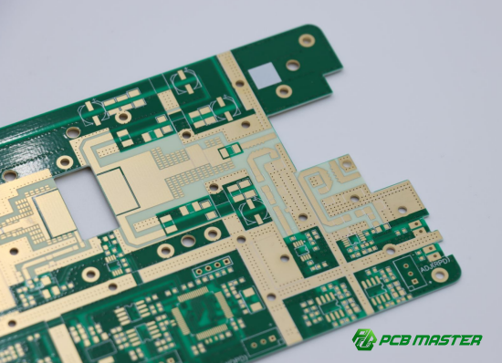
Common PCB DFM Pitfalls That Reduce Yield, Increase Cost, and Delay Production
Printed circuit board (PCB) designs often look flawless on screen, yet fail unexpectedly during fabrication or assembly. The gap between “design intent” and “manufacturing reality” is where most hidden risks emerge, quietly eroding yield, increasing cost, and extending delivery cycles.
Even experienced engineers can overlook subtle design constraints that seem minor at the schematic stage but become critical during etching, drilling, soldering, or reflow processes. These issues are not random—they typically trace back to a set of repeatable Design for Manufacturability (DFM) pitfalls embedded in layout decisions.
As product complexity increases—especially with high-density interconnects, fine-pitch components, and tighter impedance requirements—the impact of these DFM oversights becomes more pronounced. What was once a tolerable design shortcut can now trigger cascading manufacturing failures.
To bridge this gap, it is essential to examine the most common PCB DFM traps across vias, routing, solder mask, and stack-up design. The following sections break down these failure points systematically and provide practical strategies to prevent them before they reach the fabrication floor.
PCB Design DFM Via Hole Manufacturing Pitfalls: What Are the Most Common Issues?
Most via-related PCB defects come from mismatched hole size vs board thickness, incorrect via placement on pads, and insufficient clearance between vias and conductors. These issues directly reduce plating quality, solder reliability, and long-term durability.
Thick PCB vs Small Hole Diameter Causing Plating Failure
When the PCB is too thick but the via hole is too small, copper plating becomes uneven and unreliable.
In PCB manufacturing, electroplating needs space to flow evenly inside the hole. If the board thickness is high (for example, 2.0–2.4mm thick PCB) but the via hole is too small (≤0.2mm), the plating solution cannot circulate properly. This leads to thin or uneven copper on the inner wall of the via.
A common real-world failure is via barrel cracking. During thermal cycling (heating and cooling in operation), weak copper walls expand and contract unevenly, eventually breaking.
Example scenario:
- Industrial control board uses 2.4mm thick FR-4
- Designer still uses 0.15–0.2mm micro vias
- After reliability testing, multiple vias fail open circuit
Key takeaway: thicker boards require larger minimum via diameters to ensure stable plating quality in PCB manufacturing DFM rules.
Placing Vias on SMD or BGA Pads
Putting vias inside SMD or BGA (Ball Grid Array) pads reduces solder area and causes soldering defects like voids and shorts.
When a via is placed directly on a solder pad, part of the solder paste flows into the hole during reflow. This reduces the solder volume available to hold the component.
This leads to two major failures:
- Weak solder joints (cold solder / voiding): not enough solder remains on the pad
- Solder leakage into via: pad becomes “dry” after reflow
- BGA short risk: solder may bridge adjacent balls in high-density arrays
Example scenario:
- BGA 0.8mm pitch chip
- Designer places via-in-pad without filling
- After assembly, intermittent boot failure appears due to hidden voids
Best practice: Avoid via-in-pad unless necessary. If required, use via filling + copper capping (resin filled via + plated over) to maintain flat pad surface.
Insufficient Distance Between Vias and Conductors
Too little spacing between vias and traces increases leakage current risk and long-term insulation failure.
When via edges are too close to nearby copper traces, the PCB cannot maintain proper electrical isolation. Over time, moisture, dust, and voltage stress can form CAF (Conductive Anodic Filament) paths inside the PCB material.
This is especially dangerous in:
- High voltage circuits (power supply boards)
- High humidity environments (industrial, automotive)
- Long-life reliability products
Example scenario:
- Power PCB operating at 48V
- Via clearance < 0.1mm to adjacent trace
- After 3 months in humid environment, board develops intermittent short
Key impact:
- Reduced insulation resistance
- Sudden field failure
- Batch-level quality risk in mass production
Design guideline: Maintain at least ≥0.2mm via-to-copper clearance, or use blind/buried vias when space is limited.
PCB Via Design DFM Solutions and Best Manufacturing Rules
The most effective solution is aligning via design with PCB fabrication capability, avoiding via-in-pad without filling, and maintaining safe clearance rules.
To improve PCB manufacturing yield and reduce cost, engineers should follow these structured DFM rules:
1. Match hole size with board thickness
- Use PCB fab capability table before layout
- Thicker boards require larger vias for stable plating
- Avoid micro-vias on thick multilayer boards unless HDI process is used
2. Avoid via-in-pad unless fully supported
- Keep vias away from SMD/BGA pads whenever possible
- If unavoidable, apply:- Resin filling- Copper plating cap (planar surface)
- This ensures stable soldering and prevents solder loss
3. Maintain safe via clearance rules
- Minimum via-to-trace spacing: ≥0.2mm (general standard)
- Increase clearance for high voltage or automotive designs
- Use blind/buried vias when routing density is high
4. Use manufacturer capability as design baseline
- Always confirm:- minimum drill size- aspect ratio limits- plating thickness capability
- This reduces redesign cycles and improves first-pass yield
Final insight: In PCB DFM optimization, via design is not just routing—it is a manufacturing reliability decision that directly determines yield, cost, and long-term stability.
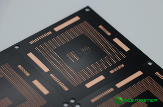
PCB Routing DFM Pitfalls: How Do They Affect Yield and Signal Performance?
PCB routing DFM issues mainly reduce manufacturing yield and degrade signal integrity by creating fabrication defects, assembly failures, and electrical performance problems such as reflection, crosstalk, and impedance mismatch.
Line Width and Spacing Too Small: How Does It Increase Manufacturing Risk?
If trace width and spacing are too small, PCB etching becomes unstable, leading to shorts, opens, and lower production yield.
In PCB manufacturing, copper is removed by chemical etching. When trace width (line width) or spacing (line-to-line distance) is too tight, the etching process cannot stay accurate. Small deviations easily cause copper bridges or broken traces.
This leads to three main risks:
- Etching residue → short circuit: leftover copper between traces connects signals unintentionally
- Over-etching → open circuit: thin traces break during production
- High voltage breakdown risk: narrow spacing cannot handle voltage stress
Real-world example:
- A power control board uses 0.1mm spacing in a standard FR4 process
- Manufacturer reports frequent copper bridging during production
- Final yield drops below 80%, causing batch rework
Key insight: Fine-pitch routing increases cost and reduces yield unless matched with advanced PCB fabrication capability (HDI or laser process).
BGA Pitch vs Pad Size Mismatch: Why Does It Cause Soldering Problems?
When BGA pitch and pad size are not properly matched, it causes solder bridging, poor soldering, and routing congestion.
BGA components require precise alignment between ball size, pitch, and pad design. If the pad is too large for a small pitch, or if routing is not optimized, solder behavior becomes unstable during reflow.
Main failure patterns:
- Solder mask opening issues: improper openings prevent clean separation between pads
- Pad too large for small pitch: reduces spacing, increasing risk of solder bridging
- Routing congestion: traces cannot escape BGA area properly
Example scenario:
- 0.4mm pitch BGA used in compact IoT device
- Designer uses oversized pads without proper fan-out design
- After assembly, multiple adjacent balls short during reflow
Key takeaway: BGA routing DFM requires strict matching between pitch, pad size, and escape routing strategy.
PCB Outline Cutting Near Pads: What Mechanical Risks Can Occur?
If traces or pads are too close to the PCB edge, mechanical cutting processes can damage copper and reduce reliability.
During CNC routing or V-cut panel separation, mechanical stress occurs near board edges. If copper features are too close, they can be physically damaged or exposed.
Main risks include:
- CNC/V-cut damage: cutting tool may scratch or cut copper traces
- Edge copper exposure: exposed copper oxidizes and degrades over time
- Assembly interference: PCB may not fit correctly into mechanical housing
Example scenario:
- Consumer device PCB has pad placed 0.1mm from board edge
- During V-cut separation, copper edge gets partially torn
- Product fails final insulation test due to exposed copper
Design rule: Maintain safe distance (typically ≥0.25mm for CNC, ≥0.4mm for V-cut depending on board thickness and process).
Impedance Trace Design Errors: How Do They Affect Signal Integrity?
Improper impedance trace design causes signal reflection, noise, and data transmission errors in high-speed PCB systems.
High-speed signals require controlled impedance. If trace geometry changes suddenly, the electrical impedance changes, which disrupts signal flow.
Main issues include:
- Width variation → impedance mismatch: signal reflects back to source
- 90° sharp bends → signal reflection and EMI increase
- Unequal differential pair spacing → timing skew and noise
Real-world example:
- DDR or USB high-speed line uses inconsistent trace width
- Signal integrity test shows data errors at high frequency
- System becomes unstable under load
Key insight: Even small routing changes can severely affect high-speed PCB signal performance.
PCB Routing DFM Optimization Guidelines: How to Improve Yield and Signal Quality?
The best optimization strategy is to follow standardized IPC rules, maintain consistent routing geometry, and match component geometry with manufacturing capability.
To improve PCB routing quality, engineers should follow these structured rules:
1. Follow IPC spacing and safety standards
- Ensure minimum trace width and spacing meet fabrication class
- Increase clearance for high-voltage circuits
- Avoid pushing design to fabrication limits
2. Match BGA design with pitch rules
- Pad size must match solder ball size and pitch
- Use proper fan-out routing for fine-pitch BGAs
- Avoid overcrowding escape routes
3. Maintain consistent impedance routing
- Keep trace width constant across the full signal path
- Avoid 90° bends; use 45° or curved routing instead
- Keep differential pairs parallel and evenly spaced
4. Validate design with manufacturing capability
- Confirm PCB fab limits before layout begins
- Run DFM checks before release
- Adjust routing rules based on process capability (standard vs HDI)
Final insight: Good PCB routing DFM is not only about drawing wires correctly—it is about ensuring manufacturability, electrical stability, and long-term reliability in real production environments.
PCB Solder Mask DFM Issues: What Hidden Risks Are Often Overlooked?
Most solder mask (solder resist) DFM problems come from poor solder mask opening design, incompatible surface finish with small pads, incorrect color selection, and improper via treatment, all of which reduce SMT yield and increase short-circuit risk.
Solder Mask Bridge Design Issues: Why Do They Cause Solder Bridging and Shorts?
If solder mask openings and bridges are not designed correctly, adjacent pads can easily connect with solder, causing short circuits during reflow.
Solder mask bridge is the thin green insulation between two copper pads. It prevents solder from flowing and connecting adjacent pads.
Common failure points:
- No solder mask opening between pads: pads are fully exposed → solder easily bridges
- Bridge too narrow: mask cannot be manufactured accurately → broken or missing bridge
- High-density BGA sensitivity: 0.4–0.5mm pitch BGAs often fail if mask clearance is not precise
Real example:
- A smartphone PCB uses 0.4mm BGA pitch
- Designer sets too small solder mask clearance
- During reflow, solder bridges form between balls → board fails functional test
Key insight: In PCB solder mask DFM, small spacing tolerance errors directly become short-circuit defects.
HASL and Small Pad Compatibility Issues: Why Does It Affect Solder Quality?
Small pads and large copper areas behave differently in HASL (hot air solder leveling) , causing uneven soldering and weak joints.
HASL is a common surface finish where solder is applied to exposed copper. However, it does not distribute evenly on all geometries.
Main risks:
- Pads smaller than 0.4mm: solder cannot fully cover → weak solder joints
- Large copper areas: act as heat sinks → solder cannot wet properly
- Oxidation risk: exposed copper without enough solder protection → poor wetting and cold joints
Example scenario:
- LED driver PCB uses large ground copper near small SMD pads
- During HASL process, heat is absorbed by copper plane
- Result: some pads show insufficient solder → intermittent LED failure
Design takeaway: For small-pitch components, consider ENIG (chemical gold) or OSP instead of HASL for better solder consistency.
Solder Mask Color Selection: How Does It Affect Manufacturing Accuracy?
Solder mask color affects manufacturing precision, especially for fine-pitch ICs, because darker or special colors reduce process stability.
Solder mask ink is not only cosmetic—it affects curing, visibility, and process control.
Key issues:
- Black or special colors: harder to control thickness → poor fine-gap performance
- Green solder mask: industry standard with highest stability and yield
- High-density IC limitation: fine pitch (<0.2mm gap) becomes difficult with non-standard colors
Real example:
- Industrial control board switches from green to black solder mask for aesthetics
- Manufacturer reports poor bridge formation consistency in BGA area
- Yield drops due to inconsistent mask openings
Key insight: PCB solder mask DFM prefers standard green for best manufacturability and lowest defect rate.
Via Opening and Solder Mask Connection Risks: Why Do They Cause SMT Failures?
When vias are improperly exposed or connected to pads, solder flows into the via, reducing solder volume and causing weak joints or voids.
Via opening (via exposure or tenting failure) is a common SMT reliability issue.
Main risks include:
- Solder wicking into via: solder flows away from pad → insufficient joint strength
- Reduced solder volume: weak mechanical connection → reliability failure
- SMT yield drop: inconsistent solder distribution across pads
Example scenario:
- BGA area has open vias near pads without filling
- During reflow, solder flows into vias
- Result: hidden voids and intermittent signal failure after assembly
Key insight: Via-in-pad or nearby via must be properly treated (filled or tented) to ensure stable SMT performance.
PCB Solder Mask DFM Optimization Strategies: How to Improve SMT Yield and Reliability?
The best approach is to standardize solder mask openings, control via treatment methods, and choose materials based on component density and process capability.
1. Standardize solder mask opening size
- Recommended: solder mask opening = pad size + 0.05mm per side
- Prevents under- or over-exposure of copper pads
- Improves consistency in mass production
2. Proper via treatment (critical in PCB DFM optimization)
- Use via tenting (cover via with solder mask) for non-critical areas
- Use via filling + capping for high-density or BGA areas
- Prevent solder loss and void formation
3. Choose solder mask color based on density level
- Green: best for fine-pitch and mass production
- Avoid black/low-contrast inks in high-density IC regions
- Ensure stable mask formation in tight geometries
4. Avoid excessive solder mask openings in dense areas
- Do not expose unnecessary copper near BGA or fine pitch ICs
- Keep mask barriers between adjacent pads whenever possible
- Reduces risk of solder bridging during reflow
Final insight: Solder mask DFM is not just a protective coating design—it is a critical factor controlling SMT yield, short-circuit prevention, and long-term PCB reliability.
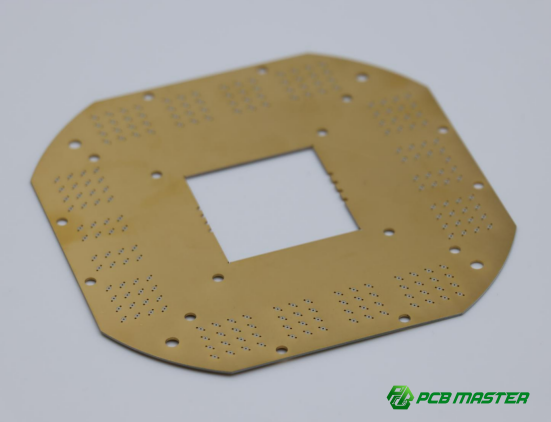
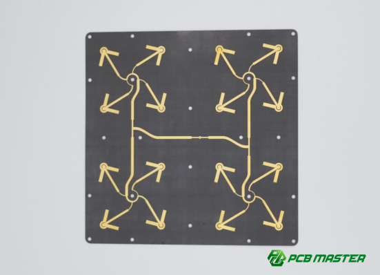
PCB Stack-Up and Panel Design DFM Issues: How Do They Affect Structural Reliability?
PCB stack-up and panel design DFM issues mainly cause board warping, mechanical cracking, assembly instability, and increased manufacturing cost due to unbalanced material structure and poor panel layout design.
Asymmetric Stack-Up Warping: Why Does Uneven Layer Design Cause PCB Deformation?
When PCB stack-up is not symmetrical, uneven copper and dielectric distribution creates internal stress, leading to board warping after reflow soldering.
In PCB stack-up DFM, symmetry is critical. If copper layers or dielectric thickness are uneven, the board expands and contracts differently during heating.
Main effects:
- Copper imbalance → internal stress: one side expands more than the other
- Reflow warping: PCB bends after high-temperature SMT process
- Automated assembly issues: SMT machines struggle with warped boards
Real-world example:
- 6-layer PCB designed with heavy copper on top layer only
- After reflow, board bends upward like a “banana”
- SMT machine fails pick-and-place alignment, causing placement errors
Key insight: Asymmetric stack-up is one of the most common PCB structural reliability failures in high-volume manufacturing.
Panel Connection Area Too Close: Why Does It Cause Mechanical Breakage?
If panel breakaway tabs or mouse bites are too close to circuits, mechanical stress during depaneling can damage traces and pads.
During PCB depaneling (separation), mechanical force is applied. If connection tabs are too close to sensitive areas, stress transfers directly into copper structures.
Main risks:
- Trace cracking: copper lines break near separation area
- Pad lifting: pads detach from substrate due to force stress
- Post-SMT failure: hidden damage appears after assembly
Example scenario:
- IoT device PCB places mouse-bite tabs only 0.2mm from signal trace
- During depaneling, slight force causes micro-crack in trace
- Device passes initial test but fails after vibration testing
Design insight: PCB panel DFM requires keeping connection points away from functional circuits.
V-Cut vs Irregular PCB Shapes: Why Do They Cause Manufacturing Conflicts?
When V-cut design is used on irregular PCB shapes, it can lead to structural weakness, assembly mismatch, or even manufacturing failure.
V-cut is designed for straight-line separation. When combined with irregular PCB outlines, problems occur.
Key issues:
- Mechanical interference: PCB cannot fit into enclosure properly
- Weak panel strength: uneven stress causes board cracking during handling
- Process limitation: some shapes cannot be routed using standard V-cut tools
Real example:
- Smart home device uses curved PCB outline
- Engineer still applies V-cut panelization
- Manufacturer cannot follow routing path → redesign required
Key takeaway: V-cut is only suitable for straight-line panel separation, not complex geometries.
Improper Panel Spacing: How Does It Increase PCB Manufacturing Cost?
Poor panel spacing reduces material utilization and machining efficiency, which directly increases PCB production cost.
Panel design is not only about fit—it directly affects cost per board.
Main cost factors:
- Low material utilization: wasted FR4 space increases cost per unit
- Reduced CNC efficiency: too many small cuts slow production
- Higher processing time: more tool paths = higher labor and machine cost
Example scenario:
- Designer leaves large unused space between small PCBs
- Panel utilization drops from 85% to 60%
- Manufacturer increases unit price due to wasted material
Key insight: Efficient PCB panel DFM directly reduces cost in mass production.
PCB Stack-Up and Panel Design Optimization: How to Improve Structural Reliability?
The best optimization approach is to design symmetric stack-ups, maintain safe panel spacing, and keep breakaway areas away from functional circuits.
1. Symmetric stack-up design (critical rule)
- Balance copper thickness on top and bottom layers
- Keep dielectric layers uniform
- Prevent thermal imbalance during reflow
2. Safe panel spacing design
- Maintain ≥2mm spacing between individual boards
- Avoid placing components near panel edges
- Improves mechanical stability during depaneling
3. Keep connection tabs away from circuits
- Minimum ≥0.6mm clearance from traces or pads
- Prevents stress transfer during breaking
- Reduces hidden micro-cracks
4. Choose correct panelization method
- Use V-cut only for straight edges
- Use routing + tabs for irregular shapes
- Match method to mechanical design requirements
Final insight: PCB stack-up and panel DFM are not just mechanical layout tasks—they directly determine board flatness, assembly success rate, and long-term product reliability in real-world applications.
How Can DFM Design Rules Systematically Reduce PCB Cost and Rework Rate?
Systematic PCB DFM (Design for Manufacturability) reduces cost and rework by aligning design with manufacturing capability, using automated verification tools, standardizing process documentation, and building a continuous feedback loop with PCB fabs.
Why Is It Important to Obtain PCB Manufacturer Capability Early?
Early access to PCB fabrication capability prevents design overruns, reduces redesign cycles, and ensures that layout rules match real manufacturing limits.
In PCB DFM optimization, the most common failure is designing beyond what the PCB factory can produce. Each manufacturer has limits such as minimum trace width, minimum spacing, and minimum drill size.
Key principles:
- Match design rules with factory capability: e.g., 0.1mm line width is not possible in standard FR4 processes
- Avoid over-designing beyond fabrication limits: reduces yield loss and scrap risk
- Reduce engineering change orders (ECO) : fewer revisions save time and cost
Real-world example:
- A startup designs a high-density board with 0.075mm trace spacing
- Selected PCB fab only supports 0.1mm minimum
- Result: full redesign required → 2-week project delay
Key insight: PCB DFM cost optimization starts before layout—at the fabrication capability alignment stage.
How Do DFM Automated Checks and Simulation Improve PCB Quality?
DFM tools and simulations detect manufacturing and signal issues before production, reducing physical prototyping failures and improving first-pass yield.
Modern PCB design uses software tools to automatically detect errors and simulate electrical behavior.
Core components:
- DRC/DFM rule check: verifies spacing, width, via size violations
- Signal integrity simulation: detects reflection, crosstalk, and delay issues
- Impedance analysis: ensures controlled impedance for high-speed signals
Example scenario:
- USB 3.0 high-speed PCB designed without impedance simulation
- DFM tool flags impedance mismatch before fabrication
- Designer adjusts trace width → avoids data error issues in production
Key takeaway: PCB DFM verification tools act as a “virtual factory” before real manufacturing begins.
Why Is Standardized Process Documentation Important in PCB Manufacturing?
Clear and standardized PCB process notes reduce misinterpretation between designers and manufacturers, improving first-pass success rate.
Many PCB failures are not design errors but communication issues. Without clear documentation, PCB fabs may misinterpret special requirements.
Key documentation practices:
- Clearly mark impedance-controlled layers: e.g., 50Ω single-ended, 100Ω differential
- Specify special via treatments: such as via-in-pad, tenting, or filling
- Define stack-up requirements explicitly: avoids guessing by fabrication team
Real-world example:
- Designer forgets to specify impedance layer in Gerber notes
- Manufacturer uses default stack-up
- Result: signal failure during high-speed testing
Key insight: Standardized PCB documentation improves manufacturing accuracy and reduces rework cycles.
How Does a Continuous DFM Feedback Loop Improve PCB Design Quality?
A DFM feedback loop collects manufacturing issues and converts them into updated design rules, continuously improving PCB quality and reducing repeat mistakes.
PCB manufacturing is iterative. Each production cycle generates valuable feedback that should be reused.
Core process:
- Collect factory feedback: yield issues, defects, assembly problems
- Convert feedback into design rules: update internal DFM checklist
- Build enterprise DFM rule library: standardized internal knowledge base
Example scenario:
- PCB fab reports repeated via solder void issues
- Engineering team updates via design rules (add tenting requirement)
- Future designs eliminate same defect automatically
Key insight: A mature DFM system evolves continuously, making each new PCB design more reliable than the last.
Hidden Cost Pitfalls in PCB DFM Design That Are Often Overlooked
The most overlooked PCB DFM hidden costs come from small design defects that scale into full-board scrap, repeated redesign cycles that delay delivery, increased manufacturing complexity that raises unit price, and supply chain limitations that reduce supplier flexibility.
How Can Small PCB DFM Issues Lead to Large-Scale Scrap Costs?
Even a small PCB defect such as a local short circuit can cause the entire production batch to be scrapped, leading to extremely high cost loss.
In PCB manufacturing, production is usually done in batches. A small design defect does not affect just one unit—it can affect the entire panel or lot.
Key cost risks:
- Local short circuit → full board scrap: one defect invalidates the entire PCB panel
- Repair cost exceeds design cost: fixing boards after assembly is often more expensive than redesigning
Real-world example:
- A 10-layer industrial PCB has a minor clearance issue in BGA area
- During production testing, repeated short circuits occur
- Entire batch of 500 boards is scrapped → thousands of dollars lost
Key insight: In PCB DFM cost management, small design mistakes scale into large manufacturing losses.
How Do PCB Rework Cycles Increase Delivery Delay Costs?
PCB design errors force engineering changes and re-fabrication, which significantly extend project timelines and delay product launches.
When DFM issues are discovered after fabrication or assembly, the design must be revised and re-submitted to the factory. This creates a full rework cycle.
Main impacts:
- Engineering redesign delays: layout changes, simulation updates, and revalidation required
- Delivery postponement: PCB re-spin adds 1–3 weeks or more per cycle
- Product launch impact: delays entire system integration schedule
Example scenario:
- Consumer device PCB fails EMC test due to routing issue
- Team must redesign and re-fabricate board
- Final product launch delayed by one month
Key insight: PCB DFM errors directly translate into project timeline risk and market delay.
Why Do Complex PCB Processes Increase Unit Cost Significantly?
Advanced PCB manufacturing features such as via filling, blind/buried vias, and controlled impedance routing significantly increase production cost.
As PCB design complexity increases, manufacturing requirements become more specialized, which increases cost per unit.
Main cost drivers:
- Via filling and plugging: requires additional processing steps and materials
- Blind/buried vias: increase drilling and lamination complexity
- Controlled impedance: requires tighter process control and testing
Example comparison:
- Standard 4-layer PCB cost: low, fast production
- HDI PCB with blind vias and impedance control: 2–5x higher cost
Key insight: PCB DFM cost optimization requires balancing performance needs with manufacturability.
How Does Supply Chain Limitation Increase PCB Manufacturing Risk?
Complex PCB processes reduce the number of capable manufacturers, increasing dependency on limited suppliers and raising delivery risk.
Not all PCB factories can produce high-complexity boards. Advanced requirements significantly narrow supplier options.
Key risks:
- Fewer qualified PCB suppliers: HDI or fine-line boards require specialized factories
- Longer lead time: limited capacity increases queue time
- Higher supply chain risk: dependency on fewer vendors
Real-world example:
- A high-density PCB requires laser drilling and microvias
- Only a few approved fabs can produce it
- Lead time increases from 7 days to 20+ days
Key insight: PCB DFM complexity directly affects supply chain flexibility and delivery stability.
How to Build a Systematic PCB DFM Checking Mechanism to Improve First-Pass Yield?
A systematic PCB DFM check system improves first-pass success by aligning design rules with manufacturing limits before layout, enforcing real-time constraints during design, using structured post-design reviews, and continuously improving rules based on production feedback.
Rule Input Stage in PCB DFM System — Why Is It Critical?
The rule input stage ensures PCB design starts with correct manufacturing limits, preventing impossible layouts and reducing redesign risk.
At the beginning of a PCB project, designers must define clear manufacturing constraints. This is the foundation of PCB DFM rule-based design.
Key actions:
- Define PCB fabrication capability limits: minimum trace width, spacing, drill size, and stack-up constraints
- Align with PCB manufacturer capability sheet: avoid designing beyond real process limits
- Build a standard design library: reuse proven layouts, pad sizes, and via structures
Example scenario:
- A company uses different PCB fabs with different capabilities
- Without rule input standardization, designers create inconsistent layouts
- Result: repeated redesigns and long approval cycles
Key insight: PCB DFM success starts before layout, not after errors appear.
How Does Real-Time DFM Constraint Checking Improve PCB Design Quality?
Real-time DFM checking prevents errors during layout by automatically detecting violations in trace width, spacing, and high-risk design areas.
Modern PCB design tools support real-time rule checking during routing. This helps engineers correct mistakes immediately instead of after completion.
Core functions:
- Line width and spacing validation: prevents unsafe routing automatically
- High-risk zone alerts: BGA, high-voltage, and impedance-controlled areas are flagged
- Instant feedback loop: designers fix issues before they become manufacturing problems
Example scenario:
- Engineer routes high-speed USB lines too close together
- DFM tool immediately flags crosstalk risk
- Routing is adjusted in real time → avoids signal failure later
Key insight: Real-time DFM is like an “automatic safety net” during PCB layout design.
Why Is Post-Design PCB DFM Review Checklist Essential?
A structured post-design review ensures all PCB manufacturing risks are checked before sending files to fabrication.
Even with real-time tools, final manual or semi-automated review is necessary to ensure no hidden issues remain.
Checklist coverage:
- Hole design review: via size, aspect ratio, via-in-pad validation
- Trace review: width, spacing, impedance compliance
- Solder mask review: openings, bridge width, via tenting
- Stack-up review: symmetry, copper balance, dielectric structure
Additional step:
- Mechanical compatibility check: ensure PCB fits enclosure and assembly fixtures
Example scenario:
- lA PCB passes routing DRC but fails due to missing solder mask clearance in BGA area
- Post-design checklist catches the issue before production
- Prevents costly re-spin
Key insight: PCB DFM review checklist acts as the final safety gate before manufacturing.
How Does Data Feedback Improve PCB DFM Optimization Over Time?
Continuous feedback from manufacturing defects helps refine PCB design rules, making future designs more reliable and cost-efficient.
PCB DFM is not static—it evolves based on real production data. Each manufacturing cycle provides valuable insights.
Core feedback loop:
- Collect production issues: shorts, opens, solder defects, warping
- Analyze root causes: design rule violations vs process limitations
- Update DFM rule library: refine constraints and best practices
Example scenario:
- Multiple boards fail due to via solder voids
- Engineering team updates rule: via tenting required in high-density areas
- Future designs eliminate the same failure mode
Key insight: PCB DFM improves continuously when manufacturing feedback is systematically integrated into design rules.
Conclusion
Ultimately, most PCB manufacturing problems are not caused by fabrication defects—they originate in the design stage. A small DFM oversight in vias, routing, solder mask design, stack-up, or panelization can quickly turn into lower yield, higher costs, production delays, and unnecessary redesign cycles.
By understanding these common PCB DFM pitfalls and building a structured review process, engineers can improve first-pass success rates, enhance product reliability, and shorten time to market. More importantly, proactive DFM practices help transform PCB design from a reactive process into a predictable and scalable manufacturing strategy.
Equally important, choosing the right manufacturing partner can make a significant difference. An experienced supplier can identify potential manufacturability issues early and provide practical recommendations before production begins. This is where PCBMASTER, a trusted PCB and PCBA supplier with extensive industry experience, can add value through professional engineering support, advanced manufacturing capabilities, and comprehensive DFM review services.
As PCB designs continue to become denser and more complex, combining sound DFM principles with expert manufacturing guidance remains one of the most effective ways to achieve higher yields, lower costs, and faster delivery.
FAQs
What is the most common PCB DFM mistake that leads to board scrap?
The most common PCB DFM mistake is placing a via directly in a solder pad or using insufficient spacing between vias and nearby conductors. These issues can cause soldering defects, electrical shorts, and CAF (Conductive Anodic Filament) failures. In mass production, even a small design error can result in an entire batch being rejected.
Why do BGA designs frequently create DFM challenges?
BGA (Ball Grid Array) components have extremely small pitch sizes, which makes the design window very limited. Solder mask openings, pad dimensions, and routing channels must all fit within a small area. If any of these elements are not optimized, problems such as solder bridging, routing congestion, and assembly defects can occur.
Does solder mask design really affect PCB manufacturing yield?
Yes. Solder mask design has a direct impact on PCB assembly quality and manufacturing yield. In high-density areas, especially around BGAs and fine-pitch ICs, poorly designed solder mask bridges can fail during production, allowing solder to connect adjacent pads and create short circuits.
How can I determine whether my PCB design matches the manufacturer's capabilities?
The best approach is to compare your design rules with the PCB manufacturer's DFM capability specifications, including minimum trace width, trace spacing, drill size, aspect ratio, and solder mask limitations. Relying only on default EDA software settings may result in designs that exceed the actual manufacturing process limits.
How much cost can PCB DFM optimization save?
The cost savings depend on the complexity of the product, but effective PCB DFM optimization can typically reduce hidden costs related to rework, scrap, and engineering changes by 20% to 50%. It can also improve first-pass yield, shorten production lead times, and reduce overall project risk.
About the Author

Carol Luo
PCB Design EngineerI'm Carol, a PCB Engineer at PCBMASTER with experience in PCB design and manufacturing engineering since 2018. I focus on translating engineering requirements into reliable PCB solutions, with expertise in stack-up design, material selection, and design-for-manufacturing (DFM). I share practical engineering insights from real-world PCB design and production experience.
Visit Carol Luo's Profile
