


PCB Cost Breakdown: How Design Choices Impact Manufacturing Expenses
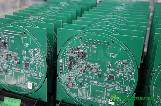
PCB cost is influenced by far more than just board size or layer count. Factors such as panelization strategy, stack-up design, material selection, surface finish, hole structures, manufacturing complexity, and quality requirements can significantly impact the final price. Understanding these cost drivers during the design phase allows engineers and procurement teams to optimize manufacturability, reduce waste, improve yields, and achieve lower overall project costs. With extensive PCB and PCBA manufacturing capabilities, PCBMASTER helps customers identify cost-saving opportunities while maintaining product reliability, quality, and delivery performance.
Understanding the Main Factors That Affect PCB Costs
Printed Circuit Boards (PCBs) are among the most important inventions in modern electronics. They connect components and enable functionality across countless products, from consumer electronics and industrial equipment to automotive systems and medical devices.
As market competition intensifies, reducing costs while maintaining quality has become a critical objective for both PCB designers and manufacturers. However, many cost increases originate during the design stage, long before production begins.
So what design choices have the greatest impact on PCB pricing? Let's examine the key cost drivers.
PCB Mechanical Design and Cost Impact
Board Size Matters
The most direct factor affecting PCB cost is board size.
Larger boards require:
- More laminate material
- Longer processing times
- Increased drilling and routing operations
- Higher shipping and storage costs
As a result, PCB pricing generally increases proportionally with board dimensions.
Optimize Panelization for Better Material Utilization
Panelization plays a major role in manufacturing efficiency.
Well-designed panel layouts can:
- Increase material utilization
- Improve SMT assembly efficiency
- Reduce handling time
- Lower production costs
At PCBMASTER, free engineering reviews help customers optimize panel layouts before production, reducing unnecessary manufacturing expenses.
V-Cut vs. Mouse Bites
When designing panelized PCBs , V-cut (V-scoring) is typically the most cost-effective depanelization method.
Benefits include:
- Higher panel utilization
- Better structural stability
- Faster separation process
- Lower manufacturing cost
For irregularly shaped boards where V-cut is not feasible, mouse bites (breakaway tabs) are commonly used.
However, designers should avoid placing tabs near:
- SMT components
- Critical traces
- Sensitive mechanical structures
Improper placement may lead to:
- Delamination
- Solder joint cracking
- Copper lifting
- Component damage during depanelization
Stack-Up Design: A Hidden Cost Multiplier
Stack-up decisions can significantly affect PCB pricing.
Excessive Dielectric Thickness
Thicker dielectric layers often require:
- Multiple prepreg sheets
- Additional lamination cycles
- Special filler materials
For example, dielectric spacing exceeding approximately 9 mil may require extra prepreg layers or even copper-free core materials, increasing material and processing costs.
Core-to-Core Lamination
Standard PCB structures typically use:
Copper Foil + Core + Copper Foil
A Core + Core construction generally costs more because it involves:
- Additional materials
- More complex lamination processes
- Lower manufacturing efficiency
Unless required for specialized applications such as RF or high-frequency designs, this structure is usually not recommended.
Non-Standard Materials
Special materials often increase procurement and manufacturing costs.
Examples include:
- Asymmetric copper laminates
- Heavy copper PCBs (2 oz and above)
- Specialty RF materials
- High-Tg laminates
- Metal-core PCBs
Asymmetrical Stack-Ups
Symmetrical stack-ups are preferred because they:
- Improve dimensional stability
- Reduce warpage
- Increase manufacturing yield
Asymmetrical constructions increase process complexity and may reduce yield rates, resulting in higher costs.
Board Thickness
Thicker PCBs require:
- More raw material
- Longer drilling times
- Additional processing controls
Generally speaking, thicker boards cost more to manufacture.
Surface Finish Selection and Pricing
Surface finish choices can significantly influence PCB cost.
Multiple Surface Finishes
Combining finishes such as:
- ENIG (Electroless Nickel Immersion Gold)
- Gold Fingers
requires additional processing steps, increasing manufacturing expenses.
Gold Thickness
For ENIG and hard gold plating:
The thicker the gold layer, the higher the cost.
Gold remains one of the most expensive materials used in PCB manufacturing.
Special Surface Finishes
Rare finishes such as Flash Gold are less common today.
Because fewer factories offer these processes, limited availability often results in higher pricing.
Other Critical PCB Cost Drivers
Drilling Complexity
The number of holes directly affects:
- Drill time
- Tool wear
- Inspection workload
More holes generally mean higher costs.
Complex Board Outlines
Intricate board shapes require:
- Additional routing operations
- Longer machine runtime
- Higher tooling costs
Advanced Manufacturing Processes
Certain technologies significantly increase PCB costs:
- Resin-filled vias
- Via-in-pad
- Blind vias
- Buried vias
- HDI structures
These processes require specialized equipment and tighter process control.
Hole Copper Thickness
Thicker plated copper inside vias requires:
- Longer plating cycles
- Increased chemical consumption
Therefore, thicker hole-wall copper increases manufacturing costs.
Restrictions on X-Out Panels
Allowing X-outs improves material utilization and yield.
When customers require:
- No X-outs
- 100% perfect panels
material utilization decreases, increasing overall production costs.
Solder Mask Color
Green solder mask remains the industry standard and most economical option.
Alternative colors such as:
- Black
- White
- Blue
- Red
- Purple
typically increase costs due to lower production volumes and additional process requirements.
Silkscreen Requirements
Special silkscreen orientations, multiple print directions, or unique marking requirements may add manufacturing complexity.
Material Grade Selection
Higher-performance materials naturally command higher prices.
Examples include:
- Automotive-grade laminates
- High-frequency materials
- High-Tg materials
- Aerospace-grade substrates
PCB Complexity and Yield
The more complex the PCB design, the greater the risk of manufacturing defects.
Lower yields often result in:
- Increased scrap rates
- Additional inspection
- Higher production costs
Acceptance Standards
Stricter quality requirements demand more extensive testing and inspection.
For example:
| Requirement | Standard PCB Production | High-Reliability Production |
| Inspection Level | Standard Testing | Enhanced Testing |
| Acceptance Criteria | IPC Class 2 | IPC Class 3 |
| Manufacturing Cost | Lower | Higher |
| Yield Requirements | Standard | More Stringent |
Organizations requiring IPC-6012 Class 3 quality standards should expect higher production costs due to tighter controls and inspection procedures.
Cost Comparison Overview
| Cost Driver | Standard Option | Higher-Cost Option |
| Panelization | V-Cut | Complex Routing |
| Surface Finish | HASL | Thick ENIG / Hard Gold |
| Layer Structure | Symmetrical | Asymmetrical |
| Copper Weight | 1 oz | 2 oz+ Heavy Copper |
| Hole Structure | Through Hole | HDI Blind/Buried Via |
| Solder Mask | Green | Custom Colors |
| Material | FR-4 | RF / High-Tg Materials |
| Quality Standard | IPC Class 2 | IPC Class 3 |
Practical Cost-Reduction Strategies
Design for Manufacturability (DFM)
Many PCB cost issues can be avoided during the design phase.
Best practices include:
- Optimize board dimensions
- Improve panel utilization
- Minimize unnecessary layer count
- Avoid excessive via structures
- Use standard materials whenever possible
- Maintain symmetrical stack-ups
Collaborate Early with Manufacturers
Early engineering reviews help identify:
- Manufacturing risks
- Yield concerns
- Material optimization opportunities
- Alternative cost-saving approaches
PCBMASTER provides free engineering file checks to ensure manufacturability, performance, and cost-effectiveness before production begins.
PCBMASTER's Approach to Cost Optimization
As a professional PCB and PCBA manufacturer serving global electronics industries, PCBMASTER combines advanced manufacturing capabilities with practical cost-control strategies.
Leveraging an 80,000㎡ manufacturing facility , PCBMASTER delivers:
- PCB fabrication
- SMT assembly
- PCBA services
- Component sourcing
- Engineering support
Supported by ISO 9001, IATF 16949, UL, and RoHS certifications , PCBMASTER ensures every project meets international quality standards.
Key Advantages
| Capability | PCBMASTER Performance |
| Quick-Turn PCB Prototype | 24 Hours |
| On-Time Delivery Rate | 99.59% |
| Product Yield Rate | 99.5% |
| Engineering Support | 50+ Engineers |
| Customer Base | 300,000+ Users |
| Service Availability | 24/7 Support |
PCBMASTER's engineering team works directly with customers to optimize stack-ups, panelization, material selection, and manufacturing processes, helping reduce unnecessary costs while maintaining product reliability.
Final Thoughts: PCB Cost Control Starts at the Design Stage
PCB costs are driven largely by material usage, manufacturing complexity, and quality requirements. While manufacturers continuously improve production efficiency, the greatest cost-saving opportunities often originate during the PCB design phase.
By considering manufacturability early, optimizing material utilization, and collaborating with experienced manufacturing partners such as PCBMASTER , companies can achieve the ideal balance between cost, quality, and performance.
As PCB technologies continue evolving toward HDI, high-frequency, automotive, and AI-driven applications, intelligent design decisions will become increasingly important for maintaining competitive advantages in both product development and manufacturing.
Tags: #PCBManufacturing #PCBA #SMTAssembly #PCBDesign #PCBMASTER #HDIPCB #RigidFlexPCB #DFM #CostOptimization #ElectronicsManufacturing #IndustryInsights
About the Author

Carol Luo
PCB Design EngineerI'm Carol, a PCB Engineer at PCBMASTER with experience in PCB design and manufacturing engineering since 2018. I focus on translating engineering requirements into reliable PCB solutions, with expertise in stack-up design, material selection, and design-for-manufacturing (DFM). I share practical engineering insights from real-world PCB design and production experience.
Visit Carol Luo's Profile
