


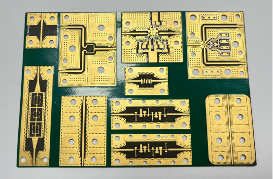
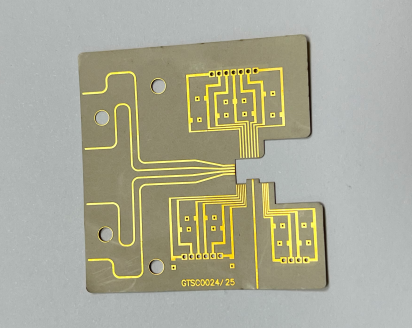
High-Frequency PCBs for RF Applications: Materials, Manufacturing, and Design
High-frequency PCBs (Printed Circuit Boards) are critical components in modern wireless communication systems. They handle RF (Radio Frequency) signals that range from 300 MHz to 300 GHz, a spectrum used by technologies like 5G, IoT devices, radar systems, and satellite communications. These signals need to travel long distances without losing power or clarity, which is where high-frequency PCBs play a crucial role.
High-frequency PCBs are designed to minimize signal loss and interference, ensuring that the RF signals remain strong and clear throughout their journey. They do this by using specialized materials and manufacturing processes that reduce energy wastage and improve signal integrity. This is particularly important for applications like 5G networks, where even small signal losses can lead to performance issues, or in radar systems where precise signals are essential.
Moreover, these PCBs help extend the lifespan of electronic devices by handling heat and electromagnetic interference (EMI) better than standard boards. By ensuring minimal signal degradation, high-frequency PCBs support the development of faster, more reliable technologies that are crucial for the next generation of wireless communication.
What Are High-Frequency PCBs and How Do They Differ from Standard PCBs?
High-frequency PCBs are specially designed boards that handle high-frequency signals in the range of 300 MHz to 300 GHz. These PCBs are used in applications where fast, reliable signal transmission is essential, such as in 5G communications, radar systems, and satellite technology. The key difference between high-frequency PCBs and standard PCBs lies in the materials used and the way they are designed to manage high-frequency signals without significant loss or distortion.
Standard PCBs are designed for lower-frequency signals (typically in the MHz range) and are made using general-purpose materials like FR4, which do not perform well at high frequencies. On the other hand, high-frequency PCBs use specialized materials like Rogers RO4003C or Megtron6, which minimize signal loss and maintain signal integrity over longer distances and higher frequencies.
Key Features of High-Frequency PCBs
Low-Loss Materials (Dk, Df)
High-frequency PCBs are made from materials with a low dielectric constant (Dk) and a low loss tangent (Df). These properties reduce the amount of signal energy lost as heat and allow the signal to travel with minimal interference. For example, Rogers RO4003C has a Dk of 3.38 and a Df of 0.0027, making it ideal for 5G and radar applications, where low signal loss is critical.
Controlled-Impedance Design
High-frequency PCBs require precise impedance control to prevent signal reflections, which can degrade the quality of the transmitted signal. By maintaining a constant impedance (typically 50Ω), high-frequency PCBs ensure that the signal travels smoothly from the source to the load, minimizing issues like signal distortion and data loss. This is especially important in high-speed communications like 5G networks.
Durability and Precision for RF Signal Integrity
The materials and design of high-frequency PCBs are engineered for durability and precision. These PCBs are built to handle high temperatures, electromagnetic interference (EMI), and mechanical stress without compromising the integrity of the RF signals. For example, using surface activated bonding (SAB) for better layer adhesion and advanced manufacturing techniques ensures that the board will function reliably over its lifetime, even under harsh conditions.
These key features make high-frequency PCBs essential for modern RF applications, offering enhanced signal quality, reliability, and performance compared to standard PCBs. By using specialized materials and precise manufacturing processes, high-frequency PCBs ensure that critical communications, such as 5G connectivity and satellite signals, remain clear and efficient.
How Do Material Choices Impact High-Frequency PCB Performance?
Material choice is key to high-frequency PCB performance. Low Dk and Df values reduce signal loss and interference, ensuring better performance in applications like 5G and radar. Poor materials can lead to signal degradation and shorter PCB lifespan, so third-party testing is essential for verifying material reliability.
Selecting Low-Loss Substrates for RF Signals
Importance of Dielectric Constant (Dk) and Loss Tangent (Df) for Signal Loss Reduction
When selecting materials for high-frequency PCBs, the dielectric constant (Dk) and loss tangent (Df) are critical factors. The dielectric constant determines how well a material can store electrical energy, while the loss tangent shows how much energy is lost as heat. Lower values of Dk and Df mean less signal loss and better performance.
For optimal signal transmission, the material should have:
Dk in the range of 2.2 to 3.6.
Df lower than 0.005.
Materials with these properties ensure minimal energy loss, allowing signals to travel longer distances without degradation. This is especially important in high-speed communications like 5G and radar, where clear signal transmission is vital.
How Material Choices Affect Signal Integrity
Effects of Poor Material Selection on Signal Degradation, EMI, and PCB Lifespan
Poor material selection in high-frequency PCBs can lead to signal degradation, electromagnetic interference (EMI), and a shorter PCB lifespan. Materials with a high Dk or Df can cause more signal loss, resulting in weaker signals and reduced performance. Inconsistent impedance and excessive EMI can further degrade the signal quality, causing errors and reducing the overall efficiency of the system.
For example, using standard FR4 material, which has a high Df (around 0.01–0.02), would lead to significant signal loss and increased interference, making it unsuitable for high-frequency applications. On the other hand, specialized materials like Rogers or Teflon, which have lower Df and Dk values, provide better signal integrity and longer-lasting performance.
Common Materials Used in RF Applications
Here’s a comparison of common materials used in RF PCBs:
| Supplier | Material | Resin Type | Dk (@10 GHz) | Df (@10 GHz) |
| AGC | TLY-5 | PTFE + Glass Fiber | 2.2 | 0.0009 |
| AGC | TLY-3 | PTFE + Glass Fiber | 2.33 | 0.0012 |
| AGC | TLX-0 | PTFE + Glass Fiber | 2.45 | 0.0012 |
| AGC | TLT-0 | PTFE + Glass Fiber | 2.45 | 0.0006 |
| AGC | TLX-8 | PTFE + Glass Fiber | 2.55 | 0.0015 |
| AGC | TLC-27 | PTFE + Glass Fiber | 2.75 | 0.003 |
| AGC | TLE-95 | PTFE + Glass Fiber | 2.95 | 0.0026 |
| AGC | TLC-30 | PTFE + Glass Fiber | 3 | 0.003 |
| AGC | TLC-32 | PTFE + Glass Fiber | 3.2 | 0.003 |
| AGC | RF-60TC | PTFE + Ceramic | 6.15 | 0.002 |
| AGC | RF-10 | PTFE + Ceramic | 10.2 | 0.0025 |
| ROGERS | RT/duroid 5880 | PTFE + Glass Fiber | 2.2 | 0.0009 |
| ROGERS | RT/duroid 5870 | PTFE + Glass Fiber | 2.33 | 0.0012 |
| ROGERS | AD250C | PTFE + Glass Fiber | 2.5 | 0.0013 |
| ROGERS | RT/duroid 6002 | PTFE + Ceramic | 2.94 | 0.0012 |
| ROGERS | AD300C | PTFE + Glass Fiber | 2.94 | 0.002 |
| ROGERS | CLTE-XT | PTFE + Glass Fiber | 2.94 | 0.0012 |
| ROGERS | RO3003 | PTFE + Ceramic | 3 | 0.001 |
| ROGERS | RO4730G3 | Hydrocarbon + Ceramic | 3 | 0.0029 |
| ROGERS | AD320A | PTFE + Glass Fiber | 3.2 | 0.0032 |
| ROGERS | TMM-3 | Hydrocarbon + Ceramic | 3.27 | 0.002 |
| ROGERS | RO4003C | Hydrocarbon + Ceramic | 3.38 | 0.0027 |
| ROGERS | RO4350B | Hydrocarbon + Ceramic | 3.48 | 0.0037 |
| ROGERS | RO4353 | Hydrocarbon + Ceramic | 3.48 | 0.0037 |
| ROGERS | AD350A | PTFE + Glass Fiber | 3.5 | 0.003 |
| ROGERS | RO3035 | PTFE + Ceramic | 3.5 | 0.0015 |
| ROGERS | TMM-4 | Hydrocarbon + Ceramic | 4.5 | 0.002 |
| ROGERS | AD450L | PTFE + Glass Fiber | 4.5 | 0.0035 |
| ROGERS | AD600L | PTFE + Glass Fiber | 6.15 | 0.003 |
| ROGERS | RO3006 | PTFE + Ceramic | 6.15 | 0.002 |
| ROGERS | RO4360G2 | Hydrocarbon + Ceramic | 6.15 | 0.0038 |
| ROGERS | RT/duroid 6006 | PTFE + Ceramic | 6.15 | 0.0027 |
| ROGERS | TMM-6 | Hydrocarbon + Ceramic | 6 | 0.0023 |
| ROGERS | TMM 10 | Hydrocarbon + Ceramic | 9.2 | 0.0022 |
| ROGERS | TMM 10i | Hydrocarbon + Ceramic | 9.8 | 0.002 |
| ROGERS | RT/duroid 6010.2LM | PTFE + Ceramic | 10.2 | 0.0023 |
| ROGERS | RO3010 | PTFE + Ceramic | 10.2 | 0.0022 |
| ROGERS | RO3210 | PTFE + Ceramic + Glass Cloth | 10.2 | 0.0027 |
| ROGERS | AD1000 | PTFE + Glass Fiber | 10.2 | 0.0023 |
| ROGERS | TMM 13i | Hydrocarbon + Ceramic | 12.85 | 0.0019 |
| SY | SCGA-500 GF220 | PTFE + Glass Fiber | 2.2 | 0.0009 |
| SY | SCGA-500 GF255 | PTFE + Glass Fiber | 2.55 | 0.0014 |
| SY | mmWave77 | PTFE + Glass Fiber | 3 | 0.001 |
| SY | AERO WAVE300 | Thermosetting Resin System | 3 | 0.0031 |
| SY | SCGA-500 GF300 | PTFE + Glass Fiber | 3 | 0.0023 |
| SY | LNB33C | Hydrocarbon + Ceramic | 3.3 | 0.003 |
| SY | S7136H | Hydrocarbon + Ceramic | 3.42 | 0.003 |
| SY | LNB33C(350) | Hydrocarbon + Ceramic | 3.5 | 0.0035 |
| SY | SGT350D | PTFE + Ceramic | 3.55 | 0.0022 |
| Wangling | F4BM220 | PTFE + Glass Fiber | 2.2 | 0.001 |
| Wangling | F4BK225 | PTFE + Glass Fiber | 2.25 | 0.0015 |
| Wangling | F4BMX245 | PTFE + Glass Fiber (Imported) | 2.45 | 0.0014 |
| Wangling | F4BME245 | PTFE + Glass Fiber | 2.45 | 0.0015 |
| Wangling | F4B255 | PTFE + Glass Fiber | 2.55 | 0.0015 |
| Wangling | F4BMX275 | PTFE + Glass Fiber | 2.75 | 0.0014 |
| Wangling | F4BME295 | PTFE + Glass Fiber | 2.95 | 0.0015 |
| Wangling | F4BM300 | PTFE + Glass Fiber | 3 | 0.0015 |
| Zhongying | ZYF220D | PTFE + Glass Fiber | 2.2 | 0.0009 |
| Zhongying | ZYF250D | PTFE + Glass Fiber | 2.5 | 0.0017 |
| Zhongying | ZYF255DA | PTFE + Glass Fiber | 2.55 | 0.0018 |
| Zhongying | ZYC8255 | Hydrocarbon + Ceramic + Glass Fiber | 2.55 | 0.0024 |
| Zhongying | ZYF300CA-C | PTFE + Ceramic | 2.94 | 0.0016 |
| Zhongying | ZYF300CA-P | PTFE + Ceramic | 3 | 0.0018 |
| Zhongying | ZYC8300 | Hydrocarbon + Ceramic | 3 | 0.0026 |
| Zhongying | ZYC8320 | Hydrocarbon + Ceramic | 3.2 | 0.0027 |
| Zhongying | ZYF320CA | PTFE + Ceramic | 3.2 | 0.003 |
| Zhongying | ZYF340CA | PTFE + Ceramic | 3.4 | 0.0033 |
| Zhongying | ZYC8340 | Hydrocarbon + Ceramic | 3.4 | 0.003 |
| Zhongying | ZYF350CA | PTFE + Ceramic | 3.5 | 0.0031 |
| Zhongying | ZYF350CA-T | PTFE + Ceramic | 3.5 | 0.002 |
| Zhongying | ZYC8350 | Hydrocarbon + Ceramic | 3.5 | 0.0032 |
| Zhongying | ZYF430CA | PTFE + Ceramic | 4.3 | 0.0034 |
| Zhongying | ZYS-P438 | PTFE + Ceramic | 4.38 | 0.001 |
Each material has its own strengths, making them suited for different applications. For example, Rogers RO4003C is ideal for 5G base stations due to its low loss and high thermal stability, while Teflon is used for ultra-high-frequency designs like mmWave because of its extremely low Df.
Real-World Testing of RF Materials
Why Third-Party Testing Data is Essential for Validating Vendor Claims
Third-party testing data is crucial for ensuring the reliability and performance of RF PCB materials. Vendor claims about material properties like Dk and Df can sometimes be inaccurate or vary in real-world conditions. Independent testing verifies that materials meet the required specifications for high-frequency applications, ensuring that the final PCB performs as expected.
For instance, Rogers and other trusted suppliers often provide third-party test results for their materials, which help manufacturers confirm the material’s true performance in real-world RF systems. This is especially important when designing complex RF systems like 5G or satellite communication, where small differences in signal loss can have a significant impact on system performance.
By requesting or reviewing third-party test data, engineers can make informed decisions about which materials will provide the best performance, minimizing the risk of signal degradation, overheating, or unexpected failures.
What Manufacturing Techniques Ensure High-Frequency PCB Reliability?
High-frequency PCB reliability is ensured through specialized techniques like laser drilling for microvias, automated inspections for defect detection, surface activated bonding (SAB) for stronger connections, and statistical process control (SPC) for consistent impedance. Quality control tests, including insertion loss (IL), return loss (RL), and thermal cycling, ensure minimal signal loss and durability, critical for applications like 5G and radar.
Specialized Manufacturing Equipment for RF PCBs
Laser Drilling: Creating Microvias for Dense Designs (5G Modules, etc.)
Laser drilling is a key technique used to create microvias—tiny, precise holes that connect different layers of a PCB. These microvias are essential for high-frequency designs like 5G modules where space is limited but the need for more connections is high. Laser drilling reduces the length of signal paths, which helps lower signal loss and electromagnetic interference (EMI). This technique is crucial for making dense, high-performance RF PCBs that maintain signal integrity at high frequencies.
Automated Optical and X-Ray Inspections: Ensuring Defect-Free Boards and Proper Inner-Layer Alignment
Automated Optical Inspection (AOI) and X-ray inspection are essential for checking the quality of PCBs during production. AOI visually inspects the surface of the board for defects such as solder bridges or misaligned components, catching 95% of defects early. X-ray inspection goes deeper, checking inner-layer alignment and solder joints, which are invisible to the naked eye. These inspections ensure that all layers of the PCB are perfectly aligned, which is critical for maintaining the signal integrity in high-frequency applications.
Surface Activated Bonding (SAB): Enhancing Peel Strength and Reducing Signal Loss
Surface Activated Bonding (SAB) is a process where plasma is used to bond LCP (Liquid Crystal Polymer) layers to copper without the need for adhesives. This method creates a strong bond with a peel strength of 800–900 g/cm, three times stronger than traditional bonding methods. The result is improved mechanical reliability and reduced signal loss due to a smoother surface. SAB is especially important in high-frequency PCBs, where every detail can impact the RF signal integrity.
Statistical Process Control (SPC): Real-Time Monitoring to Maintain Impedance Consistency
SPC is a technique used to monitor the manufacturing process in real-time, ensuring consistency across large batches of high-frequency PCBs. By tracking variables like temperature and pressure, SPC helps maintain impedance consistency within a tight tolerance, typically ±5%. This ensures that controlled-impedance traces, which are crucial for preventing signal reflections, stay accurate across thousands of units, avoiding signal degradation in 5G systems and other RF applications.
Quality Control Methods for High-Frequency PCB Manufacturing
Insertion Loss (IL) Testing: Ensuring Minimal Signal Loss (<0.7 dB/in at 10 GHz)
Insertion loss (IL) testing measures the amount of signal loss that occurs as the signal passes through the PCB. For high-frequency PCBs, the target is to keep the insertion loss below 0.7 dB/in at 10 GHz. This ensures that the board has minimal signal attenuation, which is especially important in high-speed applications like 5G or satellite communications. High-quality materials and precise manufacturing processes help achieve this low insertion loss.
Return Loss (RL) Testing: Verifying Impedance Matching to Prevent Signal Reflections
Return loss (RL) testing verifies that the PCB’s impedance is properly matched to prevent signal reflections. A return loss greater than -10 dB ensures that the board has minimal reflections, which can otherwise cause data errors and reduce performance. For RF applications, proper impedance matching is critical for maintaining signal clarity and preventing issues like phase shifts or signal degradation.
Thermal Cycling Tests: Ensuring the Board Survives Temperature Fluctuations Without Performance Degradation
Thermal cycling tests subject the PCB to repeated temperature fluctuations (e.g., -40°C to 125°C) to ensure that it can withstand extreme environmental conditions without performance degradation. For high-frequency PCBs, this test is vital as thermal expansion can cause delamination or signal loss over time. Reliable PCBs, like those from PCBMASTER, are designed to endure these fluctuations while maintaining signal integrity and long-term durability.
These manufacturing techniques and quality control methods ensure that high-frequency PCBs meet the strict demands of modern RF systems, delivering reliable performance, minimal signal loss, and long-term durability in challenging environments.
How Do You Achieve Optimal Impedance Matching in RF PCB Design?
Optimal impedance matching in RF PCB design ensures signal integrity by using 50Ω traces, impedance calculators, and the right trace geometry (microstrip or stripline). This minimizes signal loss and reflection, crucial for high-performance systems like 5G and satellite communications.
Impedance Matching: Why It’s Critical for RF Signal Integrity
Role of Controlled-Impedance (50Ω) Traces in Minimizing Signal Reflection and Loss
Impedance matching is essential in RF PCB design to ensure that the signals flow smoothly from the source (e.g., RF chip) to the load (e.g., antenna) without any signal reflection. When the impedance of the trace does not match the source or load impedance, signal reflections occur. These reflections degrade the signal quality and cause loss of data integrity. In most RF systems, the standard impedance is 50Ω. Maintaining a 50Ω controlled-impedance trace is crucial for achieving reliable and high-performance RF communication, particularly for applications like 5G and radar systems.
Techniques for Achieving 50Ω Impedance
Using Impedance Calculators: Tools like Polar SI9000 for Precise Trace Design
Achieving a 50Ω impedance requires precise calculation of the trace width and spacing. Impedance calculators, like Polar SI9000, help design traces with accurate dimensions to meet the required impedance. These tools take into account the dielectric constant (Dk) of the PCB material, the trace thickness, and the dielectric thickness to determine the correct width for the trace. For example, if you're using Rogers RO4003C, the calculator will provide the exact trace width for achieving 50Ω impedance. Using these tools helps to avoid manual errors and ensures that the board is optimized for performance.
Trace Geometry:
1. Microstrip: Surface Traces with a Ground Plane Beneath (Suitable for 1–10 GHz)
A microstrip design is a common method for achieving controlled impedance. The trace is placed on the top layer of the PCB, with a ground plane directly beneath it. This configuration works well for frequencies 1–10 GHz, as it offers good performance and is relatively easy to manufacture.
Advantages: It’s simple, cost-effective, and provides sufficient shielding for lower-frequency RF signals.
2. Stripline: Traces Sandwiched Between Ground Planes (Better for >10 GHz and mmWave)
For higher-frequency applications, like mmWave (above 10 GHz), the stripline configuration is preferred. In a stripline, the trace is sandwiched between two ground planes, offering better electromagnetic shielding. This helps reduce interference and ensures signal integrity at higher frequencies.
Advantages: Excellent for high-speed signals and reducing cross-talk and interference, making it ideal for 5G and satellite communications.
Trace Design Best Practices
1. Avoid Sharp Bends and Ensure Differential Pair Alignment for 5G Systems
Sharp bends in traces can cause signal reflections and increased loss. For high-frequency signals, it’s best to use 45° angles instead of 90° bends to reduce the impact on the signal.
Differential pairs (used in systems like 5G) must also be carefully aligned. The trace length should be matched as closely as possible to avoid phase shifts and signal mismatches.
Example: If two traces are designed for a differential pair (e.g., for 5G), they should be routed together and kept as close as possible to avoid signal skew or loss.
How Impedance Mismatch Affects Performance
Examples of How Poor Impedance Matching Impacts Signal Strength and Integrity
If impedance matching is not properly achieved, signal reflections occur, which can lead to signal degradation and data loss. For example:
In a 5G system, poor impedance matching can lead to signal distortion and reduce the data transfer speed.
In radar systems, impedance mismatch can cause false readings or missed detections, as the signal integrity is compromised.
In a satellite communication system, mismatch can cause signal interference, leading to reduced clarity and reliability in communication.
Real-World Example: A 5G base station PCB with an impedance mismatch might have signal loss of up to 1-2 dB at higher frequencies (28 GHz), which would reduce the effective communication range and speed, resulting in slower data rates for users.
What Are the Best Practices for Grounding and Shielding in High-Frequency PCBs?
Best practices for grounding and shielding in high-frequency PCBs include using solid ground planes, ground stitching vias, and single-point grounding to reduce EMI and crosstalk. Shielding techniques like metal cans and copper pour protect components and maintain signal integrity in high-performance systems like 5G.
Grounding: Minimizing EMI and Crosstalk
Importance of Solid Ground Planes and Ground Stitching Vias
Good grounding is critical for reducing electromagnetic interference (EMI) and crosstalk between signals in high-frequency PCBs. A solid ground plane provides a low-impedance path for current to flow back to the power source, minimizing noise and interference. Ground stitching vias—small connections between the ground plane and other layers of the PCB—are used to ensure a continuous ground path across the entire board. This prevents voltage fluctuations and reduces the risk of signal degradation.
Best Practices:
Cover 70%+ of unused space with copper: Ensuring most of the unused PCB area is covered with copper creates a low-impedance return path for RF signals. This helps improve signal integrity and reduces EMI by providing an optimal path for return currents.
Single-point grounding: To avoid ground loops—which occur when there are multiple paths to ground—it's crucial to use single-point grounding. This means connecting all ground connections to a single point, ensuring that there are no unintended current paths that can cause noise and interference.
Shielding Techniques for RF PCBs
Metal Shielding Cans: Protecting Sensitive Components from External Interference
Metal shielding cans are often used to protect sensitive RF components, such as 5G ICs, from external interference. These cans enclose the component and act as a barrier to prevent EMI from external sources. Metal shielding is particularly useful for high-power RF components where interference can degrade performance. The shielding can also reduce the amount of radiated EMI, ensuring that the device complies with strict electromagnetic compatibility (EMC) standards.
Copper Pour Shielding: Surrounding RF Traces with Grounded Copper for Isolation
Another effective method of shielding is copper pour shielding. In this technique, grounded copper is poured around the RF traces to isolate them from noise generated by other signals on the PCB. This approach helps reduce crosstalk—unwanted signal coupling between adjacent traces—and ensures that RF signals maintain their integrity. Copper pour is especially useful in high-density designs where space for traditional shielding cans might be limited.
Absorptive Materials: Ferrite Beads and Absorbing Foam for Damping Stray RF Energy
Absorptive materials like ferrite beads and absorbing foam are used to dampen stray RF energy that might interfere with nearby components. Ferrite beads are often placed on power lines to filter out high-frequency noise, while absorbing foam is used to reduce radiated EMI by absorbing unwanted RF signals. These materials help ensure that sensitive components, like RF transceivers, remain protected from interference.
Real-World Example: Shielding for 5G Modules
Case Study of Using Shielding Cans to Protect RF Transceivers and Reduce EMI
In 5G module design, shielding is critical for ensuring that RF transceivers work efficiently in high-density environments. For example, by using metal shielding cans around 5G ICs, designers can prevent external EMI from disrupting the signal processing. These cans effectively isolate the RF transceiver from external noise, ensuring that the module delivers high-speed communication without errors. This shielding also helps meet EMC regulations for 5G devices, ensuring compliance with industry standards.
In this case, the use of shielding cans improves signal reliability, reduces interference, and helps extend the life of the module by protecting sensitive components from thermal damage caused by heat buildup. This practice is common in high-performance applications, ensuring that 5G modules perform reliably in urban, high-interference environments.
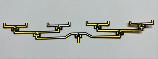
How Do You Optimize PCB Layout for RF Performance?
Optimizing PCB layout for RF performance involves minimizing trace length to reduce signal loss, strategically placing RF components to shorten signal paths, and avoiding vias that can introduce additional loss. Efficient layer stacking for dense designs helps with impedance control and signal integrity. These strategies ensure high-quality performance in 5G and other high-frequency applications.
Layout Optimization for Reduced Signal Loss
Minimizing signal loss is crucial for maintaining high RF performance in PCBs. The longer the trace length, the more signal loss occurs due to resistance and the interaction between the trace and surrounding materials. To reduce this, designers aim to keep the RF trace lengths as short as possible.
Prioritize RF traces in the layout and ensure they remain as short as possible, ideally less than 50mm for high-frequency applications like 28 GHz. This minimizes the travel distance for the RF signal, improving signal integrity and reducing attenuation.
It’s also important to ensure there are no sharp bends in the traces, as sharp turns can cause additional signal reflections that degrade performance.
By focusing on minimizing trace length, the PCB layout will have better signal quality, leading to enhanced performance in systems like 5G, Wi-Fi 6, and radar applications.
Component Placement Strategies for RF Designs
Effective component placement is essential for optimizing signal performance in RF PCBs. Proper placement reduces the distance that signals need to travel, helping maintain signal quality.
Group RF components (e.g., antennas, filters, transceivers) as closely together as possible. This minimizes trace length and helps ensure that the signal remains strong without losing power over long distances.
Avoid vias in RF paths. Vias add resistance and capacitance, leading to signal loss and reflection. If vias are unavoidable, use blind or buried vias, which do not affect the RF signal path as much as traditional through-hole vias.
By grouping related components and minimizing via usage, you ensure the RF signal remains clean and strong, improving overall system performance.
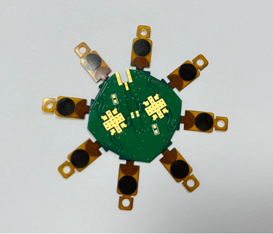
Layer Stacking for Dense RF Designs
For high-density RF designs, layer stacking plays a key role in optimizing performance. Multi-layer boards allow for more efficient routing of traces and better control over impedance.
4-layer stack-ups are suitable for moderate-density designs. The typical configuration includes top and bottom layers for RF traces, while inner layers serve as ground and power planes. This setup reduces crosstalk and ensures signal isolation.
For even denser designs, 8-layer stack-ups are ideal. These allow for more RF layers, which can be sandwiched between ground planes for better shielding and signal integrity. They are often used in 5G modules and other high-performance RF applications, where high-frequency signals need additional layers for routing and isolation.
Optimizing layer stacking not only enhances signal integrity but also improves thermal management, helping to dissipate heat generated by high-frequency signals.
What Are the Common Problems in High-Frequency PCB Design and How Can They Be Solved?
Common issues in high-frequency PCB design include signal loss, EMI, and thermal management problems. Solutions involve using low-loss materials, improving grounding, adding shielding, and managing heat with thermal vias and heat sinks. These fixes ensure better performance and reliability in RF applications.
Signal Loss (Insertion Loss)
Problem:
Signal loss, or insertion loss (IL), occurs when the RF signal weakens as it travels through the PCB. This is usually caused by poor material choices, improper trace geometry, or contamination on the PCB.
Diagnosis:
Poor material choice: Using high loss tangent materials like standard FR4 results in more energy being lost as heat, weakening the RF signal.
Improper trace geometry: If the trace is too narrow or incorrectly designed, it increases resistance and signal attenuation.
Contamination: Dust, flux residue, or other contaminants on the PCB surface can cause signal reflections and additional losses.
Solutions:
Low-loss materials: Switch to high-performance materials like Rogers RO4003C, which has a low loss tangent (Df), minimizing signal loss.
Adjust trace geometry: Use precise impedance calculators to design traces with the correct width and spacing to match the target impedance.
Clean manufacturing: Ensure PCB manufacturing is done in a cleanroom environment to avoid contaminants that can impact the signal.
By using better materials and ensuring a clean manufacturing process, you can reduce signal loss and improve overall RF signal integrity.
EMI and Crosstalk
Problem:
Electromagnetic interference (EMI) and crosstalk occur when unwanted signals interfere with the desired RF signals. This can degrade performance and cause systems to malfunction.
Diagnosis:
Grounding issues: Poor grounding can cause high impedance paths, which act as antennas and increase EMI.
Inadequate shielding: Insufficient shielding can let external interference into sensitive RF areas, leading to crosstalk between traces.
Solutions:
Improve grounding continuity: Use solid ground planes and ground stitching vias to provide a low-impedance return path, which helps reduce EMI.
Ferrite beads: Adding ferrite beads to power lines can block high-frequency noise from components like voltage regulators, preventing it from affecting RF signals.
Redesign shielding: Ensure metal shielding cans are used around sensitive components like RF transceivers. Extending these cans over ground vias and between signal traces helps block external interference and reduce crosstalk.
By improving grounding, adding ferrite beads, and enhancing shielding, you can effectively reduce EMI and crosstalk in high-frequency PCBs.
Thermal Management
Problem:
High-frequency circuits generate heat, and without effective thermal management, this heat can degrade signal integrity and lead to thermal expansion or even material failure.
Diagnosis:
Excessive heat: High-power RF components like amplifiers and oscillators generate heat that can affect the PCB material, leading to higher loss tangent (Df) and signal degradation.
Poor thermal conductivity: Using materials with low thermal conductivity can trap heat, causing thermal stress on the PCB.
Solutions:
Thermal vias: Add thermal vias directly beneath high-heat-generating components to direct heat to the ground plane for dissipation.
Heat sinks: Attach heat sinks to power-hungry components to reduce the heat generated and prevent overheating.
Better materials: Select materials like Rogers RO4003C, which have better thermal conductivity than standard FR4 to dissipate heat more efficiently.
By implementing proper thermal management solutions, such as thermal vias and heat sinks, and selecting materials with better heat dissipation properties, you can maintain signal integrity and prolong the lifespan of your high-frequency PCBs.
Conclusion
As 5G, IoT, and advanced radar systems continue to evolve, high-frequency PCBs will remain essential for ensuring seamless communication and signal integrity. These PCBs are designed to handle higher frequencies, reduce signal loss, and improve system reliability, making them a cornerstone of modern RF technology. PCBMASTER stands at the forefront of this innovation, offering specialized high-frequency PCB design and manufacturing services. Our expertise in precise impedance control, signal integrity, and low-loss materials ensures that their products meet the highest standards for applications ranging from automotive radar to medical electronics. With a commitment to advanced materials, precision manufacturing, and comprehensive quality testing, PCBMASTER helps clients achieve optimal performance in demanding environments. From prototype development to mass production, they deliver reliable, high-performance solutions that meet the needs of critical industries. Whether you're developing 5G infrastructure or satellite communications, PCBMASTER ensures your designs achieve maximum efficiency and stability.
FAQ: Common Questions About High-Frequency PCBs
What is the main difference between high-frequency PCBs and high-speed PCBs?
High-frequency PCBs and high-speed PCBs serve different purposes and are optimized for different types of signals:
High-Frequency PCBs: These are specifically designed to handle radio frequency (RF) signals typically in the range of 300 MHz to 300 GHz. RF signals, such as those used in 5G, satellite communications, radar systems, and microwave applications, require special attention to signal integrity, low loss, and minimal interference. The materials used for high-frequency PCBs, like PTFE, ceramics, and Teflon, have low dielectric constant (Dk) and low loss tangent (Df) to maintain high signal integrity over long distances.
High-Speed PCBs: These are designed to handle digital signals at speeds commonly seen in data transmission, such as PCIe 6.0, HDMI, USB, and Ethernet. High-speed PCBs focus on minimizing signal degradation due to signal reflections and crosstalk within the PCB. Materials like FR4 can be used in these designs, though low-loss variants are preferred for better performance.
In summary, high-frequency PCBs are optimized for RF signals, while high-speed PCBs handle high-speed digital signals with a focus on data transmission performance.
Can standard FR4 be used for RF applications?
No, standard FR4 is not suitable for high-frequency RF applications. Here's why:
High Dielectric Loss (Df): FR4 has a high loss tangent (Df), which means it absorbs more energy during signal transmission. This leads to signal attenuation and higher insertion loss, which is unacceptable for high-frequency signals.
Signal Degradation: The high loss in FR4 can cause significant signal degradation in applications where maintaining signal quality is critical, such as in 5G or satellite communications.
Material Alternatives: For high-frequency applications, specialized materials like Rogers, Megtron, Teflon, and ceramic-filled PTFE are preferred. These materials offer lower Df values (as low as 0.0009) and a stable dielectric constant (Dk), ensuring minimal signal loss and reflection.
Thus, to achieve the required signal integrity and reliability in RF applications, materials like Rogers RO4003C or Megtron 6 are essential, rather than standard FR4.
What is the typical cost difference between high-frequency and standard PCBs?
High-frequency PCBs typically cost 2 to 3 times more than standard FR4 PCBs. This price difference arises from several factors:
Specialized Materials: High-frequency PCBs use premium materials like Teflon, ceramics, and low-loss PTFE, which are significantly more expensive than the basic epoxy glass fibers used in FR4 boards.
Complex Manufacturing: High-frequency PCBs require precise impedance control, specialized processes, and more stringent quality control measures. These factors contribute to higher manufacturing costs.
Benefits: Despite the higher upfront cost, high-frequency PCBs offer lower signal loss, minimal reflection, and better thermal stability, which help to reduce field failures, improve system reliability, and ensure long-term performance in RF applications. Therefore, the investment in high-frequency PCBs is worthwhile for high-performance, critical applications.
What is the maximum frequency a high-frequency PCB can support?
High-frequency PCBs can support frequencies of up to 300 GHz, with the right design and materials. The frequency range depends on factors like:
Substrate Material: Materials such as Teflon and ceramic-filled PTFE can handle microwave frequencies and mmWave (up to 110 GHz and beyond).
Design Configuration: For very high frequencies (over 100 GHz), stripline and microstrip designs are used, ensuring the transmission lines are properly controlled to minimize loss and maintain signal integrity.
For applications such as mmWave communications, satellite systems, and advanced radar systems, high-frequency PCBs made with these materials and designs are capable of transmitting signals effectively at frequencies as high as 300 GHz.
How long does it take to manufacture high-frequency RF PCBs?
PCBMASTER offers rapid turnaround for high-frequency RF PCBs, with typical lead times:
Prototyping: PCBMASTER can deliver prototypes in 5–7 days, which is faster than the industry average. This allows clients to quickly test their designs and make adjustments before mass production.
Mass Production: For larger quantities, mass production takes about 15–20 days. This timeframe includes the full process of manufacturing, from material selection and etching to final testing and inspection.
This fast production schedule, coupled with a commitment to quality and reliability, ensures that customers can meet tight project timelines while maintaining the integrity and performance of their high-frequency RF applications.
Author Bio
Hi, I'm Carol, the Overseas Marketing Manager at PCBMASTER, where I focus on expanding international markets and researching PCB and PCBA solutions. Since 2020, I've been deeply involved in helping our company collaborate with global clients, addressing their technical and production needs in the PCB and PCBA sectors. Over these years, I've gained extensive experience and developed a deeper understanding of industry trends, challenges, and technological innovations.
Outside of work, I'm passionate about writing and enjoy sharing industry insights, market developments, and practical tips through my blog. I hope my posts can help you better understand the PCB and PCBA industries and maybe even offer some valuable takeaways. Of course, if you have any thoughts or questions, feel free to leave a comment below—I'd love to hear from you and discuss further!

