


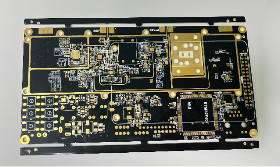
Why Backdrilling is Crucial for High-Speed PCB Design and Signal Integrity
High-speed PCB designs demand the highest level of precision, where even the smallest flaws can disrupt signal integrity. One common culprit is the unused portion of vias, or “stubs,” which can cause signal reflections, noise, and overall performance degradation. Backdrilling offers an effective solution by removing these unnecessary copper sections, ensuring signals travel smoothly and without interference. This technique has become essential in modern PCB design, where maintaining the quality of high-frequency signals is crucial for success.
What is Backdrilling?
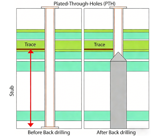
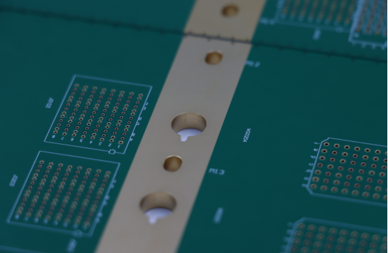
Backdrilling is a process used in printed circuit board (PCB) design to remove unwanted portions of vias (the small holes that connect different layers of a PCB). The goal is to improve signal integrity by eliminating extra copper within the via that can cause issues such as signal reflections, impedance mismatches, and unnecessary noise. By carefully drilling away this excess copper, backdrilling ensures that high-speed signals travel smoothly through the PCB, maintaining their quality.
Definition and Working Principle of Backdrilling
How does backdrilling work?
The basic process of backdrilling involves drilling from the opposite side of a via to remove unwanted copper material. In a typical multi-layer PCB, a via runs from one layer of the board to another, but in many cases, only a portion of that via is used for signal transmission. The extra copper that does not participate in the signal path can create "stubs" (short sections of unused via) that negatively affect the signal. By drilling away this unnecessary copper, the stub is removed, and the signal path is cleared.
The goal of backdrilling:
Improve Signal Integrity: Unused copper in vias can cause reflections, ringing, and signal degradation. By eliminating these stubs, backdrilling helps the signal travel with minimal interference.
Reduce Impedance and Reflection: The copper stubs in a via can create impedance mismatches. These mismatches lead to signal reflections, which distort the signal and can cause timing issues. Backdrilling reduces these reflections by removing the stubs.
For example, in a 10-layer PCB, a signal might travel from the surface layer (Layer 1) to an inner layer (Layer 3). The via might go all the way through to Layer 10, but only the copper between Layers 1 and 3 is needed for the signal. The excess copper between Layers 3 and 10 creates a stub, which could act like an antenna, interfering with the signal. Backdrilling removes this unwanted copper, ensuring the signal remains clean.
How is Backdrilling Implemented?
Process Steps:
1. Plating and Lamination: The PCB is first subjected to plating (adding copper) and lamination (layering the board with insulation and copper). This is where the via is initially formed, creating a continuous copper path from top to bottom.
2. Drilling: Once the PCB layers are completed, backdrilling is done from the opposite side of the board. This step removes the extra copper from the via that is not part of the signal path. Specialized drilling machines are used to carefully remove the copper at precise depths.
3. Controlled Depth and Position: Precision is crucial in backdrilling. The drilling depth must be accurate to avoid damaging the copper that is part of the signal path. If the depth is too shallow, the stub won't be completely removed; if it's too deep, it could damage the layers being used for signal transmission.
For instance, imagine drilling a hole through a stack of paper layers. If you drill too deep, you could go through the layers that you need to keep intact. The same principle applies to PCB backdrilling—careful control over depth ensures that only the unused copper is removed, leaving the signal path intact.
Real-World Example:
Consider a high-speed PCIe (Peripheral Component Interconnect Express) connection in a computer motherboard. PCIe signals run at very high speeds, and even the smallest imperfections in the PCB can cause issues such as jitter (timing errors) or data loss. By applying backdrilling, the extra copper in vias can be removed, reducing signal distortion and improving the overall reliability of the PCIe signal transmission.
Importance of Precision:
Backdrilling is not a simple drilling process; it requires careful control to avoid damaging the PCB. Special equipment and skilled technicians are needed to ensure that the drill stops at the exact right point to remove the unwanted copper, preventing damage to other layers. The depth and position of each drilled via are critical to ensure that only the unnecessary portions are removed without affecting the signal path.
Why is Backdrilling Crucial for Signal Integrity?
Backdrilling is vital for maintaining signal integrity in high-speed PCB designs. Without it, unwanted portions of vias—referred to as stubs—can cause several issues that affect the quality of the signal. These issues include signal reflections, interference, waveform distortion, and even bandwidth limitations.
Signal Reflection Problems: How Does It Affect Signal Quality?
Signal reflections occur when there is unused copper in a via.
When a signal travels through a via, only the portion of the via that is part of the signal path should be involved in the transmission. If there is extra copper, called a stub, it can act like an open-ended wire. This stub reflects some of the signal back toward the source, causing signal reflections. These reflections distort the original signal and can interfere with the clear transmission of data.
Effects on Time and Frequency Domains:
Time Domain: Reflections cause ringing and overshoot in the signal. This means that the signal doesn’t just go to its intended destination—it bounces back and creates echoes that can confuse the receiving system.
Frequency Domain: The signal’s frequency response is also affected. Reflections create impedance mismatches, leading to signal loss at certain frequencies, resulting in deep dips in the signal's frequency spectrum.
For example, in a high-speed data transfer, such as a 10Gbps Ethernet connection, even small reflections can lead to timing errors or lost data packets, significantly slowing down the system.
Interference and Waveform Distortion
Reflected signals distort the waveform and cause overshoot.
The reflections from the stub interact with the original signal, causing a phenomenon called waveform distortion. This happens when the reflected signal combines with the forward signal, altering its shape. Overshoot occurs when the signal spikes beyond its normal range, while ringing occurs when the signal oscillates before settling at its final value.
Impact on Eye Diagrams: Eye diagrams are used to visualize the quality of digital signals. Reflections cause the signal to degrade, leading to a closed eye pattern, which indicates poor signal quality. This results in the loss of data.
Impact on Bit Error Rate (BER): Distorted signals increase the bit error rate—the number of incorrect bits received compared to total bits transmitted. A higher BER leads to more frequent communication errors and lower system reliability.
A practical example is in DDR (Double Data Rate) memory used in computers. If the signal reflection is significant, the memory controller might misinterpret data, causing errors in data storage or retrieval. This can significantly slow down system performance and cause crashes.
Bandwidth Limitations
Stubs can reduce the bandwidth of a signal, especially at higher frequencies.
The length of the stub influences its resonance frequency—the frequency at which it naturally vibrates. When a signal’s frequency approaches this resonance, the stub starts absorbing the signal, resulting in signal attenuation (reduced signal strength). The longer the stub, the lower the resonance frequency, which leads to more pronounced attenuation at higher frequencies.
High-frequency signals like those used in PCIe (Peripheral Component Interconnect Express) or DDR memory are especially susceptible to this problem. These signals rely on very high frequencies for fast data transmission. If a stub is too long, it can cause signal loss, making the system slower or even causing communication failure.
For instance, a PCIe signal running at 16GT/s (gigatransfers per second) could suffer significant degradation if the stub within the via is not removed via backdrilling. The signal might not reach its destination in time, causing errors or delays.
Impact on Bandwidth:
Reduced Effective Bandwidth: When stubs absorb parts of the signal, the effective bandwidth decreases because the system cannot transmit data efficiently at high speeds.
System Performance: In high-speed data protocols, such as PCIe or DDR, the bandwidth limitations introduced by stubs can result in poor system performance, causing bottlenecks or failures in data processing.
Negative Effects of Stubs
In high-speed PCB design, stubs (the unused portions of vias) can have several negative impacts on signal integrity. These issues include signal reflection, increased insertion loss, crosstalk, and timing problems, all of which degrade the performance of the system.
Signal Reflection and Impedance Mismatch
Stubs act as sources of signal reflection.
When a signal travels through a via, it is intended to pass through the via and continue to the next layer without interference. However, if there is unused copper, forming a stub, this portion can reflect part of the signal back toward the source. This phenomenon is called signal reflection. The reflected signal interferes with the original signal, causing distortions such as overshoot, ringing, and incorrect signal timing.
Effect on Differential Signals:
Differential signals, which use two complementary paths for transmission, are especially sensitive to reflections. A stub can cause mode conversion, where the desired differential signal turns into unwanted common-mode noise. This noise can significantly affect the quality of the signal, especially in high-speed digital circuits.
For example, in a DDR memory system, reflections caused by stubs can cause errors in reading or writing data, leading to slowdowns and system instability. In high-frequency systems like PCIe, this signal disruption could result in data loss, reducing the performance of the entire communication channel.
Increased Insertion Loss and Crosstalk
Stubs increase insertion loss.
Insertion loss refers to the loss of signal strength as it travels through the transmission path. Stubs increase insertion loss by absorbing energy from the signal at certain frequencies, which reduces the overall power reaching the destination. The longer the stub, the more energy it absorbs, leading to more significant signal attenuation.
Example: In a high-speed Ethernet connection, even a small amount of signal loss can lead to slower data transmission or complete communication failure.
Stubs contribute to crosstalk.
Crosstalk occurs when signals from adjacent transmission paths interfere with each other. Stubs act as unwanted conductors that can create parasitic capacitance and inductance between nearby signal traces. This parasitic coupling can cause signals to leak from one path to another, creating interference that degrades signal quality.
In modern communication systems, such as USB or HDMI, crosstalk can severely affect the data integrity of high-speed signals, leading to errors, noise, and slower data rates. By removing stubs through backdrilling, these interference issues are minimized.
Timing Issues: Signal Transmission Timing Disruptions
Reflections and ringing introduce timing jitter.
When signals are reflected back due to stubs, they cause ringing—oscillations that occur after the signal has passed its peak. This results in timing jitter, where the timing of the signal’s edges (the transitions between high and low states) becomes uncertain. Jitter is problematic in high-precision systems because it reduces the available timing margin for correctly interpreting the signal.
Impact on High-Precision Timing Systems:
Timing is crucial in systems like clock signals or high-speed serial data transmission. Even small amounts of jitter can lead to misinterpretation of the signal, causing data corruption, errors, or even system failure.
Example: In high-performance computing or telecommunications systems, where clock signals synchronize multiple components, jitter can cause significant issues. If the timing isn’t precise, components may operate out of sync, leading to data loss or malfunction.
The effect of stubs on jitter is especially critical for high-speed serial links like PCIe 4.0 or Thunderbolt, where even tiny timing deviations can lead to severe system instability.
How Does Backdrilling Solve These Problems?
Backdrilling is a critical technique in high-speed PCB design that helps resolve various signal integrity issues, such as reflections, signal distortion, and timing problems. By removing unwanted copper from vias (the holes connecting different layers of the PCB), backdrilling enhances signal transmission and ensures high-quality performance, especially in high-speed applications.
The Role of Backdrilling in High-Speed Signal Transmission
How does backdrilling reduce reflections and signal distortion?
Backdrilling plays a vital role in reducing signal reflections and signal distortion caused by stubs. When there is unused copper in a via (the stub), it reflects part of the signal, which distorts the waveform and introduces errors. Backdrilling removes this excess copper, effectively eliminating the stub and preventing reflections. This results in a cleaner signal, which is crucial for high-speed data transmission.
Example: In PCIe or DDR memory applications, backdrilling ensures that the high-speed signals can travel through the PCB without interference from reflections, allowing for faster and more reliable data transfer.
How does backdrilling shorten stub length and improve signal integrity?
The key to improving signal integrity is reducing the length of the stub. The longer the stub, the greater the potential for it to act as an antenna, causing signal degradation. By backdrilling, the excess copper is removed, effectively shortening the stub length. This makes the signal path more direct and reduces the likelihood of signal loss or distortion.
Impact on Signal Integrity: A shorter stub means less chance for unwanted resonance or impedance mismatches, improving the signal's overall quality. This is especially important in high-frequency systems, where even small imperfections can significantly affect performance.
Real-World Example: Consider a high-speed USB 3.0 connection. Backdrilling ensures that the signal travels smoothly with minimal loss or distortion, allowing for faster data rates and more reliable device connections.
The Precision Requirements and Challenges of Backdrilling
How does the precision of backdrilling affect signal integrity?
Precision is crucial when performing backdrilling. If the drilling is not done accurately, there is a risk of damaging the signal path or failing to remove enough of the stub. This can negatively impact signal integrity, leading to issues such as reflections, impedance mismatches, or even complete signal failure. Therefore, backdrilling must be performed with high accuracy to avoid such problems.
Example: In advanced PCBs used for 5G communication systems, even minor imperfections caused by imprecise backdrilling can result in high-frequency signal degradation, reducing the overall performance of the system.
How is the depth and position of backdrilling controlled to avoid damaging the signal path?
Controlling the depth and position of the backdrill is critical. The goal is to remove only the unused copper without touching the parts of the via that are part of the active signal path. This requires specialized equipment and precise control to ensure that the drill stops at the exact right point. If the depth is too shallow, some of the stub may remain, and if it's too deep, the signal path could be damaged.
Step-by-Step Precision Control: Modern backdrilling machines use advanced sensors and software to monitor the drilling process in real-time. This ensures that the drill reaches the correct depth and position. The depth is usually measured in microns (thousandths of a millimeter), making it a highly precise operation.
Example: In high-speed networking equipment, where reliability is crucial, ensuring that the backdrilling process is precise prevents costly mistakes, such as signal disruptions or total communication failure between devices.
Considerations in Backdrilling Design
Designing backdrilling for high-speed PCBs requires careful consideration of various factors that can impact the quality of the signal transmission. These include the materials used, the processing techniques applied, and the best practices for optimizing signal paths.
Material Selection and Manufacturing Process
How does the choice of PCB material affect the backdrilling process?
The choice of material used in the PCB affects both the performance and efficiency of backdrilling. Different PCB materials have different properties, such as thermal expansion and electrical conductivity, which influence how easily backdrilling can be performed. Materials that are easier to drill and more stable under heat and pressure will produce better backdrilled vias, ensuring cleaner signal paths.
Example: Materials like FR4 (a commonly used fiberglass material) are easier to process compared to more complex materials like Teflon or ceramic, which are used in high-frequency applications. The higher the frequency of the signal, the more sensitive the material selection becomes.
How do different manufacturing techniques (e.g., laser drilling) apply to backdrilling?
In addition to the traditional mechanical drilling process, laser drilling has become a popular technique for backdrilling, especially for more advanced or high-density PCBs. Laser drills provide greater precision and can be used to create finer holes, ensuring that only the unnecessary copper in the via is removed.
Laser Drilling for Backdrilling: Laser backdrilling allows for controlled depth and precision, which are crucial when removing the stub without damaging the rest of the via. Laser drilling also reduces the mechanical stress on the PCB, which is particularly beneficial when working with sensitive materials.
Example: 5G antennas and high-speed memory modules require laser drilling for backdrilling due to the need for extreme accuracy in removing the stub, as even the slightest imperfection can result in signal degradation.
Best Practices for High-Speed Signal Design
How should signal paths and hole sizes be optimized in backdrilling?
Optimizing signal paths and hole sizes is essential in minimizing signal loss and ensuring clean signal transmission. The signal path should be as short and direct as possible to reduce the potential for signal degradation. Furthermore, the hole size (via diameter) plays a role in how much copper is available to remove during backdrilling. Larger holes may create more opportunities for stubs, but they also offer more space for precise backdrilling.
Signal Path Optimization: Ensuring that the signal path is as straight as possible reduces the chances of reflections or distortion. Additionally, improving the via structure (i.e., minimizing the number of vias required) can help streamline the signal flow.
Hole Size Considerations: Properly sizing vias can help reduce unnecessary copper and ensure that backdrilling is effective. Smaller vias tend to minimize stub length, which is ideal for high-speed designs. However, they require more precision to backdrill accurately.
What are common mistakes in backdrilling design, and how can they be avoided?
There are several common errors in backdrilling design that can negatively affect signal integrity. These include imprecise drilling depths, incorrect via sizes, and inadequate signal path planning.
Common Mistake 1: Incorrect Drilling Depth: One of the most frequent mistakes is not drilling the via deep enough to remove the stub completely, or drilling too deep, damaging the signal path. This can be avoided by using precise equipment and closely monitoring the depth during the backdrilling process.
Common Mistake 2: Poor Signal Path Planning: Not optimizing the signal path and via layout can lead to longer signal routes and more vias, increasing the chance for signal degradation. Using advanced simulation software can help plan the most efficient path for high-speed signals, minimizing the risk of interference.
Common Mistake 3: Inconsistent Via Sizes: Using inconsistent via sizes across different layers can lead to impedance mismatches, which cause signal reflection. It's important to standardize via sizes and ensure that backdrilling operations are performed consistently across the entire PCB.
Example: In high-frequency circuits, such as RF antennas or optical networks, the signal loss due to poor backdrilling design can lead to severe degradation of performance, resulting in slower data rates or complete system failure.
Applications of Backdrilling in Different High-Speed Signal Designs
Backdrilling is a crucial technique in the design of high-speed PCBs, especially when working with signals that require high precision and minimal interference. By removing unnecessary copper from vias, backdrilling ensures that high-speed signals travel smoothly without reflections or signal degradation.
The Importance of Backdrilling in High-Speed Digital Signal Design
Why is backdrilling critical for 10Gbps or faster signals?
High-speed digital signals, such as those used in 10Gbps Ethernet or DDR memory, require extremely high precision in their transmission. At these speeds, even tiny disruptions—such as reflections caused by stub vias—can cause significant signal degradation. For instance, signal reflections can cause data corruption or timing errors, which are detrimental to the performance of systems that rely on fast data transmission.
Backdrilling helps by removing the unused copper in the via, shortening the stub and ensuring that the signal is transmitted as cleanly and efficiently as possible. With backdrilling, high-speed signals can travel through the PCB without being affected by the negative effects of reflection, ensuring reliable data transfer at high rates.
Example: In a 10Gbps Ethernet connection, even small signal losses can cause data transmission delays, resulting in slower network speeds. Backdrilling ensures the signal travels with minimal interference, maintaining the high-speed data transfer.
How does backdrilling affect transmission stability?
Backdrilling significantly improves the transmission stability of high-speed signals. By removing the stub from vias, it reduces the potential for signal reflections and impedance mismatches, which are common sources of instability in high-speed digital signals. With less disturbance in the signal path, the transmission becomes much more stable, leading to improved performance and fewer errors.
For instance, in PCIe (Peripheral Component Interconnect Express) applications, where data transfer rates can exceed 16GT/s, maintaining a stable signal path is essential to prevent errors and ensure the system operates efficiently.
Real-World Example: In DDR memory modules, data is transferred at very high speeds. Backdrilling ensures that the signals remain stable and that the timing between data bits is maintained accurately, preventing errors in data storage and retrieval.
Backdrilling in RF Microwave Signal Applications
How does backdrilling improve RF signal quality?
Radio Frequency (RF) and microwave signals operate at much higher frequencies than digital signals, and even small imperfections in the signal path can lead to significant degradation in performance. Backdrilling is especially beneficial in RF and microwave applications because it removes stubs in vias, preventing them from acting as antenna-like structures that can interfere with the signal.
By backdrilling, the stub is shortened, preventing unwanted resonance and impedance mismatches that can distort the RF signal. This results in a cleaner signal and reduced signal loss, which is critical for maintaining the integrity of RF communication systems.
Example: In 5G communication networks, where signals are transmitted at high frequencies, backdrilling ensures that the signal remains strong and undistorted, enabling faster and more reliable connections.
What is the relationship between high-frequency signals and stubs, and how is it addressed with backdrilling?
High-frequency RF signals are especially sensitive to stubs because the length of the stub can create resonant circuits that absorb and reflect part of the signal. This resonance can cause signal attenuation (loss of signal strength) or introduce phase shifts, which disrupt the accurate transmission of RF signals.
Backdrilling addresses this problem by removing the stub and reducing the potential for these resonant effects. Shortening the stub eliminates unwanted interference and helps maintain signal strength and integrity, even at high frequencies.
Example: In microwave radar systems, where signals operate at frequencies from 1 GHz to over 100 GHz, backdrilling ensures that the signals are transmitted clearly and accurately without being affected by stub-induced resonance, ensuring the reliability of the radar’s measurements.
Conclusion
In modern PCB design, backdrilling is an essential technique for ensuring high-speed signal integrity. By removing unnecessary copper from vias, backdrilling helps eliminate signal reflections, reduces stub lengths, and improves transmission stability. This is particularly important for high-frequency signals like those used in 10Gbps Ethernet, DDR memory, and RF communication systems, where even the smallest interference can cause performance issues. As the demand for faster, more reliable circuits increases, backdrilling will continue to play a critical role in overcoming signal integrity challenges.
Looking ahead, the development of backdrilling technology will likely focus on improving precision and reducing costs. As signals continue to increase in speed, the need for more sophisticated backdrilling methods, including advanced laser techniques and integration with emerging materials, will become even more significant. At PCBMASTER, a leading PCB supplier with years of experience, we are committed to delivering high-quality products that meet these evolving demands. Our focus on precision and innovation ensures that our customers benefit from the best possible signal integrity solutions for their high-speed applications.
FAQs
1. What is the difference between backdrilling and regular drilling?
Backdrilling serves a special function by removing excess copper from vias (the holes connecting different layers of a PCB). In comparison to regular drilling, which only creates holes to facilitate electrical connections between layers, backdrilling specifically targets and removes the unused section of the via—also known as the stub—that doesn’t contribute to the signal path.
The primary role of backdrilling is to minimize signal interference caused by these unused copper sections. The presence of a stub can cause signal reflections, leading to waveform distortion, jitter, and other signal integrity issues. By eliminating the stub, backdrilling helps reduce these problems, ensuring a cleaner signal path and improving overall signal quality in high-speed applications, such as high-frequency communication or high-speed memory systems.
2. What key considerations must be taken into account when designing backdrilling?
Designing effective backdrilling requires attention to several key factors, including precision, material selection, and manufacturing processes.
Precision: Backdrilling requires extremely precise control to avoid damaging the signal path. If the depth is too shallow, the stub may remain, causing reflections. If it’s too deep, it can damage the copper needed for the active signal path.
Material Selection: Different PCB materials can affect the backdrilling process. Materials like FR4 are more common but may be easier to drill than specialized materials like Teflon or ceramic, which are often used for high-frequency applications. Choosing the right material ensures better precision and signal integrity.
Manufacturing Processes: Techniques such as laser backdrilling allow for finer control over the drilling depth and can help prevent damage to the PCB. Regular mechanical drilling may not provide the same level of accuracy, particularly for high-speed designs.
3. How does backdrilling affect the quality of high-speed signals?
Backdrilling plays a critical role in improving signal quality for high-speed designs. The most significant improvements are seen in the reduction of signal reflections and crosstalk.
Signal Reflections: When a signal passes through a via, any unused copper inside the via (the stub) can reflect part of the signal back toward the source. These reflections cause signal distortion and waveform degradation, leading to jitter and data transmission errors. Backdrilling removes these stubs, ensuring that the signal is transmitted without interference.
Crosstalk: The unused via portion can also create parasitic capacitance and inductance, which interfere with nearby signal traces, causing crosstalk. By removing the stub, backdrilling minimizes the chance of crosstalk, ensuring cleaner signal transmission and reducing interference between adjacent circuits.
In summary, backdrilling enhances signal integrity by preventing unwanted reflections and crosstalk, which is essential for maintaining high performance in high-speed digital systems.
4. How can you determine if backdrilling is necessary in a design?
The need for backdrilling depends on the application’s signal speed and the presence of via stubs that may interfere with signal integrity. Here’s how to assess whether backdrilling is necessary:
Signal Speed and Frequency: High-speed signals (such as those in 10Gbps Ethernet or DDR memory) are highly sensitive to interference. If your design involves such high-speed signals, backdrilling is often necessary to ensure clean signal transmission.
Stub Length and Signal Path: In cases where the via stub is long enough to affect signal integrity (typically above a certain frequency or data rate), backdrilling will help remove the stub and prevent issues like signal reflections and data corruption.
Simulation Tools: Using simulation tools to model the PCB can help determine if the via stub is long enough to cause problems. If the simulation indicates that stub-induced reflection is a potential issue, backdrilling should be considered.
5. How important is the precision of backdrilling?
Backdrilling precision is critical to maintaining signal integrity, timing accuracy, and bandwidth. Even minor inaccuracies in drilling depth can lead to significant problems:
Signal Integrity: Inaccurate backdrilling can leave part of the stub intact, allowing reflections to disrupt the signal. Alternatively, drilling too deep could damage the active signal path, which could completely interrupt the signal flow. This would result in severe signal degradation or failure.
Timing Accuracy (Jitter): In high-speed digital systems, precise timing is crucial. Any timing deviation caused by signal reflections or impedance mismatches can introduce jitter—small fluctuations in the signal's timing—which can degrade performance and increase bit error rates.
Bandwidth: High-speed systems require high bandwidth to transmit large amounts of data. If backdrilling isn’t performed with the necessary precision, the stub could create a resonant circuit that absorbs energy, limiting the bandwidth and reducing the overall performance of the system.
To avoid these issues, precision in backdrilling ensures that only the unnecessary stub is removed, preventing any negative impact on signal timing or bandwidth, and allowing the design to achieve optimal performance.
Author Bio
Hi, I'm Carol, the Overseas Marketing Manager at PCBMASTER, where I focus on expanding international markets and researching PCB and PCBA solutions. Since 2020, I've been deeply involved in helping our company collaborate with global clients, addressing their technical and production needs in the PCB and PCBA sectors. Over these years, I've gained extensive experience and developed a deeper understanding of industry trends, challenges, and technological innovations.
Outside of work, I'm passionate about writing and enjoy sharing industry insights, market developments, and practical tips through my blog. I hope my posts can help you better understand the PCB and PCBA industries and maybe even offer some valuable takeaways. Of course, if you have any thoughts or questions, feel free to leave a comment below—I'd love to hear from you and discuss further!

