Copper Thieving in PCBs: A Comprehensive Guide to Improving Copper Plating
Achieving uniform copper plating in PCB manufacturing is often more complicated than it first appears. Even the slightest variation in copper thickness can lead to serious issues, affecting both performance and production efficiency. Enter copper thieving—an essential technique that addresses these challenges by ensuring consistent plating across the entire board. While it may not be directly involved in the circuit itself, its role in the manufacturing process is indispensable, boosting yields and enhancing overall design quality. Let’s dive into how this seemingly simple strategy can make a world of difference in your PCB production.
Introduction to Copper Thieving
What is Copper Thieving in PCB Manufacturing?
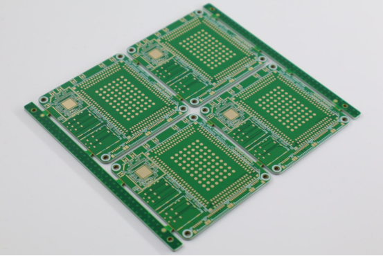
Copper thieving is a technique used in PCB manufacturing to add small, non-functional copper shapes in empty areas of a circuit board. These shapes ensure uniform copper plating, preventing defects like uneven copper thickness and poor etching.
Overview of Copper Thieving and Its Role in Improving PCB Plating and Etching Processes
Copper thieving improves the copper plating process by adding small copper features to empty spaces on a PCB. Without these features, the electroplating current can become uneven, leading to over-plating in empty areas and under-plating near traces. By using copper thieving, the current is distributed more evenly, ensuring consistent copper thickness across the entire board.
Purpose and Importance in Maintaining Uniform Copper Thickness on PCBs
Copper thieving ensures that the copper layer is evenly distributed, which is crucial for the board’s electrical performance and durability. Uneven plating can result in weak connections, short circuits, or open circuits. Copper thieving prevents these issues by maintaining uniform copper thickness, which is especially important for high-precision PCBs like HDI boards.
Why Copper Thieving is Necessary in PCB Manufacturing
Copper thieving is necessary to ensure even copper plating by balancing the current flow during electroplating, preventing over-plating and under-plating that could cause defects.
Impact of Empty Spaces on Electroplating
Empty spaces on a PCB cause the electroplating current to flow unevenly, leading to over-plating in those areas. This creates problems when etching the PCB later, as over-plated areas may cause short circuits, while under-plated areas result in weak, thin traces.
The Challenge of Uneven Current Distribution
Without copper thieving, the electroplating current isn’t evenly distributed across the PCB, causing some areas to receive too much copper (over-plating) and others too little (under-plating). Both situations lead to defects that can affect the final product’s quality and reliability.
Copper Thieving as a Solution
Copper thieving solves this by adding small copper shapes in empty areas, helping distribute the plating current more evenly. This results in uniform copper thickness and prevents plating defects, ensuring a high-quality finished PCB.
What Are the Key Functions of Copper Thieving in PCB Manufacturing?
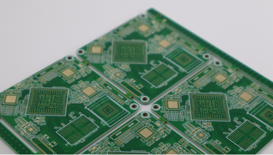
Copper thieving serves three primary functions in PCB manufacturing: improving plating uniformity, preventing plating defects, and enhancing etching consistency. These functions help ensure high-quality, reliable PCBs with even copper layers and precise trace dimensions.
1. Improvement of Plating Uniformity
In PCB manufacturing, electroplating is used to apply a copper layer onto the board. However, areas without traces or components—referred to as “dead zones”—tend to have an uneven flow of plating current. This can result in uneven copper thickness, causing areas to become too thick (over-plating) or too thin (under-plating). Copper thieving helps solve this by placing small, non-functional copper shapes in these empty regions. These shapes spread out the plating current more evenly, ensuring that the copper thickness is consistent across the entire PCB. For example, in a PCB with a large empty space between components, adding copper thieving ensures the plating process is more uniform, preventing problems caused by uneven current distribution.
2. Prevention of Plating Defects
Over-plating occurs when areas of the PCB, particularly those without traces, receive too much copper. This leads to thick copper regions that are difficult to etch and can result in short circuits or electrical failures. Under-plating, on the other hand, happens when areas with traces don’t receive enough copper, making the traces weak and prone to breaking under stress. Copper thieving addresses both of these issues. By placing copper dots or other shapes in the empty areas, the plating current is distributed more evenly, preventing over-plating and ensuring that all areas of the board receive the correct amount of copper. This is particularly important for high-precision PCBs, where even small variations in copper thickness can cause failure. For instance, in high-frequency circuit boards, any excess copper could affect signal integrity, while insufficient copper could lead to unreliable performance.
3. Enhancement of Etching Consistency
Etching is the process used to remove excess copper from the PCB after electroplating, leaving behind the desired circuit pattern. If the copper layer is uneven, etching can be inconsistent, resulting in defects. Over-plated areas are harder to etch and may leave behind unwanted copper, while under-plated areas may etch too quickly, leading to weak or broken traces. Copper thieving helps mitigate this issue by ensuring that the copper layer is even across the entire board. The copper shapes added in the empty spaces help balance the current distribution during plating, resulting in a more uniform layer of copper that can be etched cleanly. For example, in multi-layer PCBs, thieving ensures that the copper thickness on each layer is consistent, preventing etching defects that could compromise the integrity of the final product.
Why Is Copper Thieving Necessary in PCB Production?
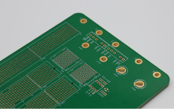
Copper thieving is necessary in PCB production to prevent plating issues like over-plating and under-plating, which arise due to large empty areas on the board. By balancing the current flow, copper thieving ensures uniform copper thickness, improving the overall quality of the PCB.
1. Impact of Empty Spaces on Electroplating
In PCB manufacturing, electroplating is the process of applying a layer of copper to the board. However, when there are large empty spaces—areas without components or traces—the current can flow in an unbalanced manner. These empty areas, known as "dead zones," allow the plating current to concentrate, leading to over-plating in those regions. Over-plating results in thick copper layers, which can be difficult to etch and may cause short circuits or defects.
On the other hand, areas with dense traces or components might not receive enough current during the electroplating process, leading to under-plating. Under-plating results in thinner copper layers that weaken the PCB's traces and may cause them to break under stress. Copper thieving helps solve this problem by filling these empty spaces with small copper features, ensuring an even current flow and uniform copper distribution.
For instance, a PCB with a large gap between a microcontroller and a connector would benefit from copper thieving. By adding small copper shapes (like dots or grids) in the empty space, the plating current can be distributed evenly, preventing the over-plating in the gap and under-plating near the dense areas.
2. The Challenge of Uneven Current Distribution
Electroplating relies on the even distribution of current to achieve a consistent copper layer across the entire PCB. However, when there are varying densities of copper features on the board, the current can flow unevenly. Empty areas (with no traces or components) act as low-resistance paths, allowing more current to flow through them, which can cause over-plating. Trace-heavy areas create more resistance, limiting the current flow and potentially leading to under-plating.
This imbalance can cause significant issues during the production process. Over-plated areas are difficult to etch and might leave behind excess copper, while under-plated areas may have weak copper layers that are prone to failure. For example, in multi-layer PCBs where precision is essential, any imbalance in plating can lead to malfunctioning circuits or even complete board failure. Copper thieving helps address these issues by creating an even current flow across the entire board, ensuring that each area is plated correctly.
3. Copper Thieving as a Solution
Copper thieving is an effective solution to the problem of uneven current distribution during electroplating. By adding non-functional copper features (like dots, grids, or small copper blocks) to empty spaces on the PCB, the plating current is spread more evenly across the board. These shapes do not connect to the circuit and do not interfere with the board's functionality, but they help equalize the current flow.
When copper thieving is applied, the empty spaces no longer create low-resistance paths for the current, preventing over-plating in these areas. At the same time, it ensures that trace-rich areas receive adequate current for proper plating. For example, in a PCB with a large empty section near the edge, thieving shapes will be placed in that area, ensuring that the copper layer is as thick and even as in the more densely populated sections.
Copper thieving is especially useful in high-precision applications like HDI (High-Density Interconnector) boards, where even a small variation in copper thickness can cause significant issues. By using copper thieving, manufacturers can maintain consistent copper layers, preventing defects like weak traces or excessive copper build-up that might cause shorts.
How Does Copper Thieving Work in PCB Design?
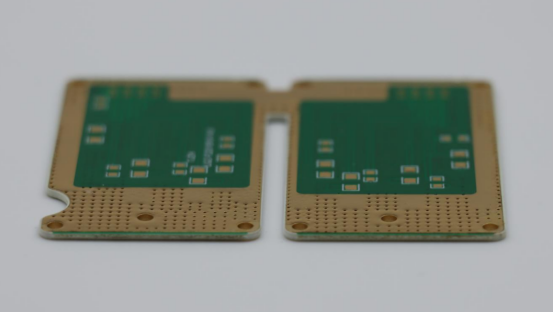
Copper thieving is a step-by-step process used in PCB design to add small copper shapes to empty areas, ensuring uniform copper plating. It involves identifying empty spaces, adding thieving patterns, ensuring isolation from active components, and validating the design through DFM checks.
1. Step 1: Identification of Empty Spaces in the PCB Design
In the PCB design process, it's essential to find large areas that have no components or traces. These areas are referred to as "dead zones." Dead zones can lead to problems in electroplating, as they cause the plating current to become uneven. To identify these areas, PCB designers use design software tools such as Altium Designer, Eagle, or KiCad. These tools help pinpoint regions larger than a specified size (e.g., 5mm x 5mm) that are free from active components like traces and pads.
Designers can also use Design Rule Checks (DRC) to automatically highlight these empty spaces. Once identified, these regions are flagged for copper thieving, ensuring that they won't interfere with the electroplating process. For example, in a PCB design where the space between a microprocessor and other components is too large, it can be marked as a "dead zone" requiring thieving to balance current flow during plating.
2. Step 2: Addition of Thieving Patterns
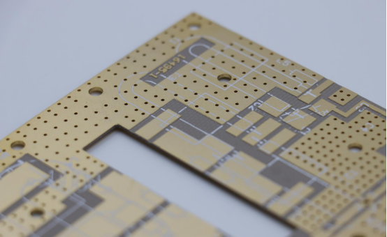
Once the empty spaces are detected, the next step is to add copper thieving patterns. These patterns are non-functional copper shapes that do not connect to the circuit's active elements but are crucial for improving plating uniformity. The most common types of thieving patterns include:
Dots: Small circular copper shapes, usually 0.5–2mm in diameter. Dots are the most versatile and commonly used for small empty areas.
Grids: Square-shaped copper patterns placed in grid formations, typically with 0.2–0.5mm spacing between them. These are ideal for larger empty areas.
Solid Blocks: Larger copper fills, such as 2mm × 2mm, are used to fill narrow gaps between traces, preventing plating imbalance in smaller spaces.
For instance, a PCB design with a large empty gap between a processor and a connector might use a grid pattern to fill the space evenly. This ensures that the copper plating process remains balanced, avoiding the issues caused by empty areas.
3. Step 3: Ensuring Isolation of Thieving Shapes from Active Circuitry
While copper thieving is essential for even plating, it’s equally important to isolate the thieving shapes from the active parts of the PCB, such as signal traces, pads, and planes. Thieving patterns should be placed at least 0.2mm away from these active areas to prevent accidental shorts or signal interference.
If thieving patterns are placed too close to active circuitry, they might cause unwanted electrical connections or disrupt signal paths. This is especially crucial in high-frequency PCBs where even a small interference could lead to signal degradation or malfunction.
For example, if a thieving dot is placed too close to a signal trace, it could create an unintended connection, causing a short circuit or altering the signal path. Therefore, careful attention must be given to maintain the appropriate spacing between thieving shapes and active components.
4. Step 4: Validation Through DFM Checks
Once copper thieving patterns are added to the design, it’s crucial to verify that the patterns comply with the manufacturing capabilities. DFM tools in PCB design software, such as Altium Designer’s DFM check or KiCad’s built-in rules checker, are used to ensure that the thieving shapes meet essential requirements, such as minimum size, spacing, and isolation from active components.
These tools automatically check the PCB design to make sure that the thieving patterns will not cause issues during manufacturing. For example, DFM checks will confirm if the spacing between thieving patterns and traces is sufficient, and if the shapes are large enough to ensure effective current distribution during electroplating.
By using DFM checks, designers can catch potential errors early in the design process, avoiding costly revisions or production delays. A design that passes DFM validation ensures that the copper thieving process will work smoothly in the production phase, leading to high-quality, reliable PCBs.
What Are the Pros and Cons of Using Copper Thieving?
Copper thieving offers several benefits, such as improved copper thickness uniformity, increased production yield, and cost-effectiveness. However, it also has some challenges, including added design complexity, potential signal interference, and a possible increase in design file size.
Benefits of Copper Thieving in PCB Manufacturing
1. Improved Uniformity of Copper Thickness Across the PCB
One of the main advantages of copper thieving is that it helps achieve uniform copper thickness across the entire PCB. In the electroplating process, areas with no components or traces can cause uneven current flow, leading to over-plating in empty areas and under-plating in dense regions. By adding copper thieving patterns, current flow is more evenly distributed, ensuring that the copper layer is consistent throughout the board. This uniformity is crucial for creating PCBs that function well, especially in high-performance applications like HDI (High-Density Interconnector) boards, where even small variations in copper thickness can lead to failures.
2. Increased Production Yield and Reduced Defects
Copper thieving plays a significant role in improving production yields and reducing defects. By ensuring uniform copper plating, copper thieving helps prevent common issues like over-plating and under-plating, which can cause shorts, weak traces, or open circuits. With fewer defects, manufacturers experience a higher success rate in producing fully functional PCBs. This reduction in defects leads to lower rejection rates, meaning that more PCBs pass quality control, ultimately increasing the overall production yield. For example, in a large batch of PCBs, those that use copper thieving are less likely to have plating-related defects, ensuring that more boards meet the desired standards.
3. Cost-effectiveness Due to the Use of Existing Copper Layers
Copper thieving does not require any extra materials, making it a cost-effective solution for improving plating quality. Since it uses the same copper layers already part of the PCB design, manufacturers don’t have to invest in additional copper or expensive materials. This saves money on material costs, especially when working with high-volume production runs. Moreover, copper thieving can help reduce the costs associated with reworking or repairing defective boards, as it minimizes the chance of plating issues that would otherwise require additional resources to fix.
Drawbacks and Challenges of Copper Thieving
1. Complexity Added to the Design Process
While copper thieving provides numerous benefits, it also increases design complexity. Designers must carefully identify empty areas that require thieving, choose the right type of thieving pattern (dots, grids, or blocks), and ensure that the patterns do not interfere with active components. Additionally, copper thieving requires more time and attention to detail during the design phase, which can increase the overall workload. For example, adding and validating thieving patterns using Design for Manufacturability (DFM) tools requires extra steps to ensure that the thieving doesn’t create electrical issues or violate manufacturing rules. As a result, the design process becomes more involved and time-consuming.
2. Risk of Signal Interference and Circuit Issues if Not Correctly Implemented
One of the potential drawbacks of copper thieving is that, if not properly isolated from active circuitry (such as signal traces and pads), it can cause signal interference or circuit issues. Thieving patterns should always be placed with a minimum distance (typically 0.2mm) from active areas to avoid unintended electrical connections. If thieving shapes are too close to signal traces, they can alter the signal path, cause shorts, or lead to crosstalk in high-frequency circuits. This can be especially problematic in sensitive applications, such as high-speed digital or analog PCBs, where signal integrity is critical.
3. Potential Increase in Design File Size
Copper thieving introduces additional small copper shapes into the PCB design, which increases the overall design file size. As more thieving patterns are added, the file becomes more complex, which may slow down the performance of design software and make the file harder to manage. In large, complex PCB designs, the increased file size can affect the efficiency of collaboration, simulation, and analysis processes. For example, designers may experience slower rendering times or difficulty in making quick changes to the layout due to the added complexity. Additionally, larger design files can slow down the manufacturing process if the files need to be processed multiple times.
When Should Copper Thieving Be Used in PCB Design?
Copper thieving is most useful in PCB designs that have large empty areas, high-precision requirements, or varying trace densities. It ensures uniform copper plating, making it ideal for power supply circuits, HDI boards, and designs where consistent copper thickness is crucial for component reliability.
Ideal Applications for Copper Thieving
1. Large Empty Areas with No Components, Especially in Power Supply Circuits
In power supply circuits, there are often large empty spaces between sections like the AC input and DC output. These areas, with no active components or traces, can cause uneven copper plating during electroplating, leading to over-plating in the empty regions. Copper thieving helps solve this by adding small copper shapes to these spaces, ensuring that plating current is evenly distributed and the copper layer is uniform. For example, a PCB used in a power supply system might have an empty section between the rectifier and the voltage regulator. Copper thieving would fill that gap with non-functional copper patterns, improving plating consistency.
2. High-Precision PCBs, Such as HDI Boards, with Fine-Pitch Traces
In high-precision applications, such as HDI boards used in smartphones or medical devices, the copper layer thickness must be very precise. Even slight variations in copper thickness can cause issues like signal interference or broken traces. HDI boards typically have dense and fine-pitch traces that require careful attention to plating uniformity. Copper thieving ensures that areas without traces receive consistent plating, preventing over-plating or under-plating that could affect the performance of fine-pitch traces. For instance, in a smartphone PCB, where traces as thin as 0.1mm are common, copper thieving helps maintain the precision needed for reliable operation.
Scenarios Where Thieving Is Particularly Useful
1. Single-Layer and Multilayer Boards with Varying Trace Density
PCBs with uneven trace density, whether single-layer or multilayer, face challenges in the electroplating process. In areas where traces are dense, current flow is restricted, leading to under-plating, while in areas with fewer traces, the current flows too freely, causing over-plating. Copper thieving helps balance the current distribution across these regions, ensuring even plating. For example, in a single-layer PCB used in a simple device, the spaces between densely packed components can cause uneven copper deposition. Copper thieving fills those gaps with small copper patterns to make the plating process uniform. This approach works the same way in multilayer boards, where different layers might have varying trace densities.
2. PCBs Where Consistent Copper Plating Is Critical to Component Reliability
In high-reliability industries like aerospace, automotive, or medical electronics, the performance of PCBs heavily depends on the consistency of copper plating. Variations in copper thickness can lead to weak electrical connections, signal integrity issues, or even component failure under high stress. Copper thieving helps maintain uniform plating, especially in areas without traces or components, ensuring that all parts of the PCB are robust and functional. For example, in a medical device PCB, where component reliability is critical, copper thieving ensures that the copper layer is uniformly applied, reducing the chances of electrical failures or poor connections.
What Are the Best Practices for Implementing Copper Thieving in PCBs?
To successfully implement copper thieving in PCBs, it is important to select the right thieving pattern, maintain proper spacing between thieving shapes and traces, and utilize Design for Manufacturability (DFM) tools to validate the design. These best practices ensure uniform copper plating and prevent common issues such as interference and manufacturing defects.
1. Optimal Thieving Pattern Selection
Selecting the appropriate thieving pattern is crucial to achieving effective copper plating. The most common types of thieving shapes are dots, grids, and solid blocks.
When choosing a thieving pattern, consider the size of the empty area and the density of the surrounding circuitry. For example, in a power supply PCB, where there might be larger empty spaces, using a grid pattern would be effective for filling those spaces without overcrowding the design. For HDI boards, which require fine control over copper thickness, using smaller dots can help maintain precision.
2. Correct Spacing to Prevent Interference
Maintaining proper spacing between thieving shapes and the active components (such as signal traces and pads) is crucial to avoid unwanted electrical connections or interference. Thieving patterns should be placed far enough from active traces to prevent issues like short circuits or signal interference, particularly in high-frequency circuits.
The recommended minimum spacing is typically 0.2mm. If thieving shapes are placed too close to sensitive areas, they might interfere with the circuit's functionality. For example, in high-speed digital PCBs used in computers or mobile devices, even small interference can disrupt signals and cause malfunctions. Thus, it is important to position thieving patterns carefully, ensuring they do not impact the path of high-frequency signals.
Real-Life Example: In a medical device PCB, where reliability is critical, ensuring that the thieving patterns are correctly spaced from the signal traces prevents any possibility of circuit failure or signal degradation.
3. Utilizing DFM Tools for Thieving Validation
After implementing copper thieving patterns, it’s essential to validate the design using DFM tools within PCB design software (such as Altium Designer, KiCad, or Eagle). DFM tools automatically check the design for errors or potential manufacturing issues, including ensuring that thieving patterns comply with the minimum size, spacing requirements, and other industry standards.
Steps for DFM Validation:
Check Pattern Size and Spacing: DFM tools will verify that the thieving patterns are of the correct size and that they are properly spaced from active components to avoid interference or shorts.
Ensure Plating Compliance: DFM checks confirm that the thieving patterns will result in consistent copper plating, preventing issues like over-plating or under-plating during electroplating.
Simulate Manufacturing Process: Some DFM tools simulate the manufacturing process to predict potential issues and optimize the design for real-world production.
By using these tools, designers can avoid costly production errors and reduce the chances of defects, ensuring that the PCB will perform reliably in its final application.
Example: In a high-precision PCB used in aerospace applications, DFM tools can ensure that the thieving patterns are correctly implemented to maintain the structural integrity of the PCB during the rigorous manufacturing process.
What Are the Common Mistakes to Avoid When Using Copper Thieving?
Common mistakes when using copper thieving in PCB design include placing thieving shapes too close to active circuit elements, choosing inefficient thieving patterns, and ignoring DFM checks. These errors can lead to issues like signal interference, uneven plating, and manufacturing defects.
1. Placing Thieving Shapes Too Close to Active Circuit Elements
One of the biggest mistakes in copper thieving is placing thieving shapes too close to active circuit elements, such as signal traces, pads, or planes. If thieving shapes are positioned too near these elements, it can result in unwanted electrical connections or short circuits. This is especially critical in high-speed or high-frequency circuits, where even a slight interference can disrupt the entire system.
The ideal minimum distance between thieving shapes and active circuitry is generally 0.2mm to 0.5mm, depending on the design rules of the PCB manufacturer. Failing to maintain this distance increases the risk of signal degradation or unintended shorts, which can cause the PCB to malfunction. For example, in a smartphone PCB, where precision is key, incorrect placement of thieving could cause communication failures between components, leading to system errors or device malfunctions.
2. Choosing Inefficient Thieving Patterns
Choosing the wrong type of thieving pattern is another common mistake. Not all thieving patterns are suitable for every PCB design. If the thieving shapes are too large or too small for the empty spaces, the plating may still be uneven. For example:
Too few thieving patterns may not provide enough coverage, causing under-plating in areas with little or no traces.
Too many thieving patterns in small spaces can lead to over-plating, causing copper buildup that makes subsequent etching difficult, leading to defects like open circuits or trace thinning.
The key is to choose an appropriate thieving shape—such as dots, grids, or solid blocks—based on the size of the empty space and the density of surrounding components. For instance, using dots for small gaps and grids for larger empty areas ensures that current flows evenly, leading to uniform copper thickness. An inefficient thieving design might make the electroplating process more difficult or lead to manufacturing defects, resulting in additional costs or board rework.
Real-Life Example: In high-density interconnect (HDI) boards, where fine-pitch traces are common, inefficient thieving patterns can cause plating variations that affect trace width and lead to functionality issues, such as signal loss or trace breakage.
3. Ignoring DFM Checks
Another critical mistake is ignoring DFM checks when designing PCBs with copper thieving. DFM tools in PCB design software are designed to help identify potential issues before the design moves to production. These tools ensure that thieving patterns meet key manufacturing specifications, including minimum size, spacing, and compliance with electroplating rules.
By bypassing DFM checks, designers risk submitting a design that is not manufacturable, resulting in production delays or having to go back to the drawing board. Without DFM validation, thieving patterns might not be properly sized or spaced, leading to defects like over-plating, under-plating, or improper copper distribution.
For example, if a thieving pattern is too small or too close to traces, it may be flagged by DFM tools. Skipping these checks could mean that the PCB will not pass the manufacturing process, requiring costly rework or leading to the rejection of entire batches. This is especially important in high-volume PCB production, where catching these issues early can save significant time and costs.
Real-Life Example: In a medical device PCB, where the failure of a single component can lead to critical issues, ignoring DFM checks could result in defects that might go unnoticed until after manufacturing, compromising the quality and safety of the device.
Conclusion
Copper thieving is a vital technique in PCB manufacturing that ensures uniform copper plating and the overall reliability of the final product. By filling empty spaces with non-functional copper shapes, it balances current distribution during electroplating, preventing common issues like over-plating and under-plating. This process is especially crucial in high-precision applications such as HDI boards and power supply circuits, where consistent copper thickness is key to performance and durability. Copper thieving also boosts production yields, reducing the likelihood of defects and increasing manufacturing efficiency.
Used across a wide range of PCB types, from single-layer boards to multilayer HDI designs, copper thieving is a versatile and cost-effective solution that enhances the quality of both simple and complex circuits. Its widespread application in industries like consumer electronics, automotive, and medical devices highlights its importance in ensuring high-performance, reliable PCBs.
If you have further questions or would like more information about PCB manufacturing, feel free to reach out to PCBMASTER. As an experienced PCB supplier, we are always ready to provide expert insights and assist with your design and production needs.
FAQs
What happens if copper thieving is not used in PCB design?
If copper thieving is not used in PCB design, the electroplating process can become uneven, leading to significant issues. Large, empty areas on the PCB, such as gaps between components or sections without traces, become "low-resistance paths" during the plating process. This causes the plating current to focus too much on these areas, resulting in over-plating. In contrast, regions with dense traces and components receive too little current, leading to under-plating. These plating defects can cause thick copper areas, which are harder to etch, and thin copper regions, which may fail under stress or create weak electrical connections. Over time, these plating inconsistencies can compromise the reliability and performance of the PCB.
Can copper thieving affect the electrical performance of a PCB?
Well-placed copper thieving will not affect the electrical performance of the PCB. Copper thieving shapes are non-functional and isolated from the active circuit, meaning they don’t carry signals or power. They only serve to improve plating uniformity during manufacturing. However, poorly placed thieving can cause problems. If thieving shapes are too close to active circuit elements, such as signal traces, pads, or planes, they might create unwanted electrical connections, causing short circuits or signal interference. This can lead to malfunctioning circuits or degraded performance. Therefore, proper design, ensuring sufficient spacing between thieving shapes and active components, is key to avoiding these issues.
Is copper thieving applicable to all PCB types?
Yes, copper thieving is applicable to all PCB types, including single-layer, multilayer, and HDI boards.
Single-layer boards often have large areas with no traces or components, making them ideal candidates for copper thieving to ensure uniform copper plating.
Multilayer boards, with their varying trace densities and internal layers, benefit from thieving to maintain consistent copper thickness throughout the board.
HDI (High-Density Interconnector) boards require precise copper thickness for fine-pitch traces, and copper thieving helps to achieve this by balancing the plating process in regions with few or no traces.
In short, copper thieving is a versatile solution that can be used effectively across different types of PCBs to enhance manufacturing quality and reliability.
How much does copper thieving affect the overall cost of PCB production?
Copper thieving is a cost-effective solution for PCB production. Since copper thieving uses the existing copper layers on the board, there are no additional material costs involved. The process only requires some extra design steps to incorporate thieving patterns, which are relatively simple to implement in PCB design software. Furthermore, by ensuring uniform plating, copper thieving reduces defects like over- or under-plating, which can lead to costly rework or scrap. This ultimately improves yield, making copper thieving a cost-effective method to enhance PCB production quality without significant additional expense.
How do I know if my PCB design requires copper thieving?
You should consider copper thieving in your PCB design if your board has large, empty areas with no components or traces, especially if these areas are over 5mm x 5mm in size. Copper thieving is particularly beneficial in situations where you want to ensure even copper plating, such as in power supply PCBs, HDI boards, or designs with varying trace densities. If your PCB design has gaps between components that could lead to plating inconsistencies, thieving patterns can help distribute the plating current more evenly across the board. Additionally, if you’re designing for high-reliability applications, such as medical devices or aerospace components, copper thieving can ensure the overall integrity of the PCB by preventing plating defects. You can use DFM (Design for Manufacturability) tools to validate whether copper thieving is required and ensure your design meets manufacturing standards.
Author Bio
Hi, I'm Carol, the Overseas Marketing Manager at PCBMASTER, where I focus on expanding international markets and researching PCB and PCBA solutions. Since 2020, I've been deeply involved in helping our company collaborate with global clients, addressing their technical and production needs in the PCB and PCBA sectors. Over these years, I've gained extensive experience and developed a deeper understanding of industry trends, challenges, and technological innovations.
Outside of work, I'm passionate about writing and enjoy sharing industry insights, market developments, and practical tips through my blog. I hope my posts can help you better understand the PCB and PCBA industries and maybe even offer some valuable takeaways. Of course, if you have any thoughts or questions, feel free to leave a comment below—I'd love to hear from you and discuss further!