


How to Address High Aspect Ratio Challenges in PCB Manufacturing
As electronic devices continue to shrink in size and increase in performance, the demand for advanced packaging technologies, such as 2.5D/3D ICs and Chiplet integration, has soared. However, this progress brings with it a significant challenge: the creation of high aspect ratio PCBs. These components, with their deep, narrow holes, require precision manufacturing techniques to ensure optimal functionality. The difficulties lie not just in creating these holes, but in ensuring the integrity of their metal coatings, cleaning them effectively, and detecting defects that may remain hidden to the naked eye. Tackling these obstacles requires a deep understanding of advanced techniques and materials, each addressing a unique aspect of the process. Let’s dive into the solutions driving the evolution of high aspect ratio PCB manufacturing.
Why High Aspect Ratio is a Key Challenge in PCB Manufacturing?
High aspect ratio holes are crucial in advanced PCB designs but pose significant challenges. Their depth and narrowness make processes like electroplating, cleaning, and defect detection more complex, requiring specialized techniques to ensure quality and reliability.
What is High Aspect Ratio and How is it Applied?
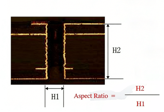
Definition of High Aspect Ratio:
A high aspect ratio in PCB manufacturing refers to holes or vias with a depth significantly greater than their diameter. Typically, a ratio greater than 10:1 or even 15:1 is considered high. This means that for every 10 or 15 units of depth, the hole’s diameter is just 1 unit. These deep, narrow holes are required in many advanced electronic devices, where space is limited but high-performance components are needed.
Applications of High Aspect Ratio:
High aspect ratio holes are particularly critical in advanced packaging technologies like 2.5D and 3D ICs and Chiplet integration. These technologies involve stacking or connecting multiple chips in a compact, high-density format to enhance performance. High aspect ratio vias are needed to make electrical connections between these layers of chips, but creating them reliably poses significant manufacturing challenges.
Manufacturing Challenges of High Aspect Ratio
Uneven Electroplating:
One of the primary challenges in high aspect ratio PCB manufacturing is achieving even electroplating inside narrow, deep holes. During the electroplating process, metal is deposited onto the walls of the hole. However, the electroplating tends to be thicker at the hole opening and thinner at the bottom due to the geometry of the hole. This uneven plating can lead to weak connections, poor electrical performance, and even failure.
To overcome this challenge, techniques like pulse plating are used, where the current is reversed periodically to prevent thick plating at the hole opening, ensuring a more uniform layer of metal.
Cleaning Difficulties:
Another challenge with high aspect ratio holes is cleaning. After drilling the holes, remnants of material, such as resin or metal debris, can get trapped inside. These residues can affect the quality of the subsequent electroplating, as well as create areas prone to corrosion or failure. The cleaning process needs to ensure that no residue is left behind, and this can be particularly difficult for narrow, deep holes.
Effective cleaning methods include plasma cleaning, where a gas like oxygen is ionized to remove organic materials from the surface. Vacuum-assisted cleaning and ultrasonic cleaning are also commonly used to ensure all debris is removed from hard-to-reach areas inside the holes.
Unreliable Filling and Risk of Voids:
Filling the deep holes with metal can also be problematic. Voids or empty spaces may form within the hole during the filling process, leading to unreliable connections. These voids are particularly problematic because they can create weak spots in the PCB, causing electrical failure over time.
The use of super-filling electroplating techniques, where metal is deposited faster at the bottom of the hole than at the edges, helps reduce the formation of voids. This method ensures that the hole is completely filled from bottom to top without gaps or air pockets.
Detection Difficulties:
Finally, detecting defects inside high aspect ratio holes is a significant challenge. Traditional inspection methods, such as visual inspection, cannot easily identify problems inside these narrow, deep holes. Hidden defects like voids, cracks, or incomplete plating can go unnoticed until after the PCB has been assembled and starts to fail.
To overcome this, non-destructive testing methods like 3D X-ray microscopy are used. These technologies can look inside the holes and generate detailed images to check for issues like voids or incomplete fills. Ultrasonic scanning is also used to detect defects by measuring sound wave reflections within the PCB.
How Electroplating Technologies Address High Aspect Ratio Challenges
Electroplating plays a crucial role in overcoming the challenges of high aspect ratio holes in PCB manufacturing. These deep, narrow holes require precise metal deposition to ensure uniformity and reliability. Advanced electroplating techniques, such as pulse plating, special chemical additives, and super-filling technologies, are designed to address issues like uneven plating, voids, and poor filling, ensuring high-quality, durable connections in complex PCB designs.
How Does Pulse Electroplating Improve Plating Uniformity?
Pulse Electroplating Explained:
Pulse electroplating is a technique where the direction of the current used to deposit metal alternates periodically. By reversing the current at regular intervals, the process helps achieve a more uniform coating inside deep, narrow holes—common in high aspect ratio PCB manufacturing.
Effectiveness in High Aspect Ratio Holes:
In traditional electroplating, metal tends to build up faster at the edges of holes, leading to uneven deposits. Pulse electroplating, however, forces the current to focus more on the bottom of the hole, which helps prevent over-deposition near the hole's opening. This results in a more even layer of metal throughout the hole, reducing the risk of weak connections and improving the overall reliability of the PCB.
Advantages:
Better Uniformity: Pulse plating ensures that metal is deposited evenly throughout the entire hole, from top to bottom.
Prevention of Over-deposition: It reduces the likelihood of thick plating at the hole entrance, which can create weak spots.
Enhanced Reliability: By achieving more uniform plating, pulse electroplating helps improve the electrical and mechanical performance of the PCB.
How Do Special Additives and Chemical Solutions Improve Deposition in High Aspect Ratio Holes?
High-Dispersibility and Leveling Electroplating Liquids:
Special additives are used in electroplating solutions to improve metal deposition inside high aspect ratio holes. These additives enhance the dispersibility of the plating solution, allowing it to flow more easily into deep holes. They also improve the leveling ability of the solution, which means it can create a smooth, even surface inside the holes, even at great depths.
How It Helps in High Aspect Ratio Deposition:
Dispersibility ensures that the electroplating solution reaches all parts of the hole, especially the bottom, which is harder to reach in deep holes.
Leveling ability ensures that the metal inside the hole is deposited evenly, avoiding the formation of uneven layers or voids.
Chemical Copper Plating as a Foundation for Electroplating:
Chemical copper plating is often used as a preparatory step before the main electroplating process. This process involves depositing a thin layer of copper chemically, rather than by electric current. This chemical copper layer ensures good conductivity and provides a smooth surface for the subsequent electroplating process, improving the adhesion and uniformity of the metal deposits inside high aspect ratio holes.
Advantages:
Improved Filling and Coverage: Additives improve how well the electroplating solution covers the hole and ensures it fills the entire depth evenly.
Better Adhesion: Chemical copper plating provides a smooth surface for better metal adhesion, which improves the overall reliability of the final PCB.
How Does Super-Filling and Bottom-Up Electroplating Prevent Voids in High Aspect Ratio Holes?
Super-Filling Electroplating:
Super-filling is a special technique that ensures metal fills deep holes without leaving voids (empty spaces). Unlike traditional electroplating, where metal deposits more on the edges than at the bottom, super-filling uses a combination of additives that promote faster deposition at the bottom of the hole. This ensures that the hole fills from the bottom up, minimizing the risk of air pockets or voids forming inside.
How It Prevents Voids:
The super-filling process helps to achieve bottom-up deposition, meaning the metal fills the hole starting from the deepest point and gradually working its way up to the surface. This method eliminates gaps or voids, which are common issues in high aspect ratio electroplating.
Role of Organic Additives (Inhibitors, Accelerators, and Levelers):
Inhibitors: Slow down the plating process at the edges of the hole, preventing over-deposition.
Accelerators: Speed up the deposition at the bottom of the hole, ensuring faster filling at the deepest part.
Levelers: Help ensure an even distribution of the plating, smoothing out any irregularities in the deposited metal.
These additives work together to improve the overall quality and uniformity of the metal fill, ensuring that high aspect ratio holes are filled reliably from top to bottom.
Advantages:
Eliminates Voids: Ensures complete metal fill, with no air pockets or gaps.
Improved Reliability: Bottom-up filling creates more reliable electrical connections, reducing the chance of failure.
Enhanced Performance: By filling holes completely, super-filling improves the overall performance of the PCB, especially in high-density applications.
How Cleaning and Residue Removal Ensure Metallization Quality
Cleaning and residue removal are critical steps in ensuring the quality of metallization in PCB manufacturing. Any leftover contaminants, such as resin or organic materials, can interfere with the electroplating process, leading to weak connections or poor performance. Advanced cleaning techniques like plasma cleaning, vacuum-assisted cleaning, and ultrasonic cleaning help ensure that high aspect ratio holes are thoroughly cleaned, providing a clean surface for proper metal adhesion and reliable functionality.
What Role Does Plasma Cleaning Play in Removing Residue and Organic Contaminants?
Plasma Cleaning Explained:
Plasma cleaning uses ionized gases (plasma) to clean surfaces by breaking down organic materials like resin residues and other contaminants inside PCB holes. The process involves exposing the PCB to a plasma field, which is generated by applying a high voltage to gases such as oxygen (O₂), carbon tetrafluoride (CF₄), or a mix of argon (Ar) and hydrogen (H₂). The plasma interacts with the surface, removing contaminants at the molecular level.
How Plasma Removes Residues:
Plasma cleaning is effective because it uses highly energetic ions and free radicals to break apart and dissolve organic materials. For instance, oxygen plasma reacts with organic substances to convert them into gas, which is then easily removed from the surface. This process is especially useful for cleaning hard-to-reach areas within deep, narrow holes.
Effects of O₂/CF₄ or Ar/H₂ Mixture:
O₂/CF₄ mixture is particularly effective at breaking down carbon-based residues, such as adhesives or resin, that remain inside holes after drilling.
Ar/H₂ mixtures are more effective in etching or cleaning the metallic surfaces, ensuring better adhesion for subsequent layers of plating or coatings.
Advantages:
Thorough Cleaning: Plasma can reach all areas of the hole, ensuring no residue is left behind.
High Efficiency: Plasma cleaning is fast and effective at removing even the smallest organic molecules that traditional cleaning methods might miss.
Minimal Damage: Plasma treatment is non-abrasive, ensuring that the PCB structure remains intact.
What Are the Advantages of Improved Wet Cleaning Methods?
Vacuum-Assisted Cleaning
Vacuum-assisted cleaning involves applying a vacuum during the cleaning process to help remove contaminants from deep within the holes. By reducing air pressure, the cleaning solution can penetrate deeper into the holes, displacing air pockets and removing stubborn residues more effectively.
How It Improves Cleaning:
The vacuum creates a pressure differential, which encourages the cleaning solution to flow more effectively into tight spaces. This action helps remove trapped air and residues from inside narrow holes, ensuring thorough cleaning before electroplating or other processes.
Advantages:
Deeper Penetration: The vacuum improves the ability of the cleaning solution to reach areas that might otherwise remain dirty.
Better Residue Removal: It effectively removes air pockets and residues trapped deep within holes, improving the overall quality of the metalization.
Ultrasonic Cleaning
Ultrasonic cleaning uses high-frequency sound waves to create microscopic bubbles in a cleaning solution. These bubbles implode when they reach the surface, generating intense scrubbing action that helps dislodge dirt and residues from surfaces. The process is especially useful for removing fine particles and organic residues inside deep vias.
How It Enhances Cleaning:
The sound waves generate rapid pressure changes that create tiny bubbles, which generate intense cleaning force when they collapse. This helps remove even the smallest particles and organic contaminants that could interfere with the electroplating process.
Advantages:
Effective for Fine Residues: The microscopic bubbles are excellent at removing particles as small as 1-2 microns.
Non-Abrasive: The process is gentle on the PCB surface, ensuring that delicate structures are not damaged during cleaning.
Enhanced Cleaning Speed: Ultrasonic cleaning speeds up the cleaning process by allowing for more thorough residue removal.
Alternating Acidic and Alkaline Cleaning Solutions
An alternating use of acidic and alkaline solutions is a cleaning strategy that helps tackle different types of contaminants. Acidic solutions are good for dissolving metal oxides, while alkaline solutions are more effective for breaking down organic residues. By alternating between these solutions, manufacturers can ensure a more thorough and complete cleaning process.
How It Works:
Acidic Solutions: Remove oxidation or metallic contamination that might have built up during drilling or plating.
Alkaline Solutions: Break down organic substances, such as resin residues, oils, or adhesives.
Advantages:
Complete Cleaning: Using both types of solutions ensures that all types of contaminants are effectively removed.
Improved Metallization: Thorough cleaning with both acidic and alkaline solutions ensures that the metal plating adheres properly to the PCB surface, improving the quality and reliability of the final product.
How to Improve Hole Wall Quality During the Drilling Process
Improving hole wall quality is crucial for ensuring the reliability and performance of PCBs. Whether through laser drilling or mechanical drilling, the process must minimize damage, heat, and debris to create precise, smooth holes. By using advanced techniques like UV lasers and optimizing drilling parameters, manufacturers can achieve high-quality hole walls, essential for high-performance electronic devices.
What Are the Advantages of Laser Drilling Technology?
Laser Drilling Explained:
Laser drilling, especially using ultraviolet (UV) and femtosecond lasers, is a highly precise method for creating small holes in PCBs, especially in high aspect ratio designs. This technique uses focused laser light to vaporize material, creating clean and accurate holes without physical contact.
Reducing Heat-Affected Zone and Improving Hole Wall Precision:
The primary advantage of UV and femtosecond lasers is their ability to minimize the heat-affected zone (HAZ) around the drilled hole. Traditional methods like mechanical drilling generate heat, which can cause the surrounding material to melt or burn, creating rough edges and uneven hole walls. However, UV and femtosecond lasers produce very short pulses of light that minimize heat generation, reducing the risk of material deformation and preserving the integrity of the hole's walls. This results in more precise, cleaner holes with smooth, high-quality walls, ideal for advanced PCB designs requiring high accuracy.
Reducing Debris and Carbonization:
Another key benefit of laser drilling is the ability to reduce molten debris or carbonization around the hole. When drilling through certain materials, heat can cause the material to melt and form unwanted residues that can negatively impact the quality of the hole. Using multi-pulse laser control, the laser delivers pulses in a controlled manner, which minimizes the amount of heat produced and reduces the risk of molten material sticking to the hole walls. This process significantly lowers the occurrence of carbonization and helps maintain a clean hole structure.
Advantages of Laser Drilling:
Precise Holes: Laser drilling offers high accuracy with minimal wall damage.
Reduced Thermal Damage: The reduced heat-affected zone keeps the material intact, ensuring better hole quality.
Minimal Debris: The laser’s controlled pulses reduce molten debris and carbonization, leading to cleaner holes.
How Does Optimizing Mechanical Drilling Improve Hole Wall Quality?
Mechanical Drilling Optimization:
Mechanical drilling is another common method used for creating holes in PCBs. While laser drilling is ideal for smaller, more precise holes, mechanical drilling is often used for larger holes. To improve hole wall quality, it’s essential to use high-precision micro-drills and optimize the drilling parameters, such as rotation speed, feed rate, and tool material.
High-Precision Micro-Drills and Optimized Parameters:
High-precision micro-drills with sharp tips are crucial for achieving smooth, clean hole walls. These drills are designed to create holes with minimal friction, reducing the risk of wall damage. Additionally, adjusting the drill rotation speed and feed rate helps to control the amount of pressure applied during the drilling process. This balance ensures that the drill penetrates the material cleanly, without creating rough edges or excessive heat buildup.
By carefully selecting drill materials that are harder and more durable, the drilling process becomes more efficient and less likely to produce damaged hole walls. Using carbide or diamond-coated drills for particularly tough materials helps maintain precision throughout the drilling process.
Optimizing Drilling Parameters for Hole Wall Quality:
Rotation Speed: Proper rotation speed ensures the drill cuts smoothly, preventing excessive force and heat.
Feed Rate: Adjusting the feed rate prevents the drill from pushing too hard, which can lead to rough or jagged hole walls.
Tool Material: The use of harder drill materials like carbide helps maintain sharpness and precision.
Advantages of Optimized Mechanical Drilling:
Precise and Smooth Holes: High-precision drills and optimized parameters create holes with smooth, consistent walls.
Reduced Wall Damage: Proper parameter adjustments prevent excessive heat buildup and pressure, reducing the risk of damaging the hole.
Improved Quality for Larger Holes: Mechanical drilling is more suitable for larger holes and can be optimized for improved quality.
What Are the Detection and Quality Control Strategies in High Aspect Ratio PCB Manufacturing?
In high aspect ratio PCB manufacturing, ensuring the quality and reliability of the final product requires advanced detection and quality control strategies. Both non-destructive methods, like 3D X-ray microscopy and scanning ultrasound, and destructive techniques, such as FIB-SEM and metallographic cross-sectioning, are used to detect defects and verify the integrity of metal fills, hole walls, and layers. These methods help identify potential issues early, ensuring high-performance, defect-free PCBs.
What Are the Key Non-Destructive Testing Methods?
3D X-Ray Microscopy for Assessing Hole Fill and Plating Uniformity:
How 3D X-Ray Microscopy Works:
3D X-ray microscopy is an advanced imaging technique used to inspect the internal structures of PCBs without causing any damage. By using X-rays, this method can capture detailed three-dimensional images of the holes inside a PCB, allowing engineers to assess both metal fill and plating uniformity.
How It Evaluates Hole Fill and Plating:
This method provides a comprehensive view of the hole’s internal structure, including whether it is completely filled with metal and whether the plating is uniform along the walls and bottom of the hole. In high aspect ratio holes, where traditional visual inspection cannot reach, 3D X-ray microscopy can detect potential issues like voids, incomplete filling, or uneven plating, which are crucial for the PCB’s electrical and mechanical reliability.
Advantages of 3D X-Ray Microscopy:
Detailed Imaging: Provides high-resolution, 3D images of internal structures, making it easier to detect defects that are not visible externally.
Non-Destructive: Does not damage the PCB, making it ideal for quality control in high-value, high-performance PCBs.
Accurate Assessment: It helps ensure that metal fills are uniform, reducing the risk of weak electrical connections.
Scanning Acoustic Microscopy for Voids and Layer Defects:
How Scanning Ultrasound Works:
Scanning ultrasound microscopy, or scanning acoustic microscopy (SAM), uses high-frequency sound waves to inspect internal structures. The sound waves are directed into the PCB, and their reflections are used to create detailed images of the internal features, such as voids and layer separations.
How It Detects Voids and Layer Defects:
SAM is especially effective in identifying voids, which are small pockets of air or empty spaces that may remain after the metal filling process. Voids inside the hole can lead to poor electrical connections and are a common problem in high aspect ratio PCBs. SAM also detects delamination or layer separation, which can affect the overall integrity of the PCB. By analyzing how sound waves interact with the material, it can identify internal defects that are not visible to the naked eye.
Advantages of Scanning Ultrasound:
High Sensitivity to Voids: Very effective at detecting tiny air pockets or gaps that can cause failure.
Layer Integrity Checking: Helps verify the integrity of the PCB layers, ensuring no separation or delamination.
Non-Destructive: Like 3D X-ray, SAM does not damage the PCB during inspection.
What Are the Key Destructive Testing Methods?
Focused Ion Beam (FIB) and Scanning Electron Microscopy (SEM) for Micro Analysis:
How FIB and SEM Work Together:
The focused ion beam (FIB) technique involves using a highly focused beam of ions to mill or cut through the material at a microscopic level. Once a sample is prepared, scanning electron microscopy (SEM) is used to observe the detailed structure of the cut surface. The combination of these two techniques allows for detailed, high-resolution imaging and analysis of specific areas of interest on a PCB.
How They Assist in Process Validation:
FIB-SEM is ideal for process validation, as it allows engineers to analyze microstructures of materials at a very fine scale. It helps identify issues like poor metal adhesion, incomplete fills, or layer separation that may not be detected through non-destructive methods. This micro-level analysis provides crucial data for troubleshooting and improving manufacturing processes.
Advantages of FIB and SEM:
High Resolution: Provides incredibly detailed images of even the smallest features on a PCB.
Micro-Scale Analysis: Perfect for investigating minute defects that affect the performance and reliability of the PCB.
Process Validation: Allows engineers to verify that the manufacturing process is achieving the desired results at a microscopic level.
Metallographic Cross-Sectioning for Reliability Testing:
How Metallographic Cross-Sectioning Works:
Metallographic cross-sectioning is a traditional but highly reliable method for inspecting the internal structure of a PCB. The process involves slicing the PCB into thin sections, then polishing and examining the cut surface under a microscope to assess the material’s internal characteristics.
How It Ensures Reliability:
This technique is used to validate the quality of metal fills, plating uniformity, and the overall integrity of the hole walls and layers. By examining the cross-section, engineers can detect issues such as voids, delamination, and improper metal deposition. It also allows for detailed analysis of material properties, ensuring the PCB meets quality standards.
Advantages of Metallographic Cross-Sectioning:
Reliable and Traditional: A tried-and-true method for verifying the physical integrity of PCBs.
In-Depth Analysis: Provides a clear, detailed view of the material structure, allowing for precise identification of potential issues.
Verification of Process Results: Useful for validating that manufacturing processes are producing the desired outcomes.
How to Optimize Materials and Design in High Aspect Ratio PCBs?
Optimizing materials and design is essential for improving the performance and manufacturability of high aspect ratio PCBs. By selecting low roughness and high homogeneity materials like ABF, PI, and modified epoxy, you can enhance hole wall quality and ensure more reliable metal filling. Additionally, design adjustments such as increasing hole diameter and using blind and buried vias help reduce aspect ratio, making the PCB easier to manufacture while maintaining high performance.
How Does Choosing the Right Materials Improve Hole Wall Quality?
Selecting Materials with Low Roughness and High Homogeneity:
When designing high aspect ratio PCBs, the choice of material plays a crucial role in improving hole wall quality. Materials with low surface roughness and high homogeneity, such as ABF (Anhydride-Butyl-Formaldehyde), PI (Polyimide), and modified epoxy resins, are ideal for creating smoother and more reliable hole walls.
How These Materials Help:
Low Roughness: Materials with lower surface roughness provide smoother hole walls. This ensures a better finish during processes like electroplating, where the metal deposits more evenly. A smoother surface reduces the likelihood of defects such as uneven metal fill or poor adhesion.
High Homogeneity: Materials with high homogeneity have a consistent internal structure, which prevents issues such as delamination or layer separation during drilling. This uniformity ensures that the hole walls remain intact during and after the manufacturing process, improving overall PCB integrity.
Advantages of These Materials:
Improved Plating: With smoother, more uniform hole walls, electroplating processes are more consistent, reducing defects.
Better Durability: These materials are more resistant to stress and thermal cycling, ensuring the holes and overall PCB remain reliable over time.
Enhanced Hole Quality: Materials like PI and ABF have good electrical and thermal properties, which are beneficial for high-density and high-performance applications.
How Can Design Optimization Reduce Aspect Ratio?
Optimizing Design to Reduce Aspect Ratio:
Reducing the aspect ratio (the ratio of the hole’s depth to its diameter) is a key strategy in improving PCB manufacturability and performance. The lower the aspect ratio, the easier it is to achieve uniform metal filling and plating, which enhances the overall reliability of the PCB.
Ways to Reduce Aspect Ratio:
Increase Hole Diameter: By increasing the hole's diameter, the depth-to-diameter ratio decreases, lowering the aspect ratio. Larger holes are easier to fill evenly during the electroplating process, reducing the risk of voids or incomplete fills.
Adjust Hole Spacing: Properly adjusting the hole pitch (distance between holes) also reduces the overall aspect ratio. More spaced-out holes allow for better manufacturing processes and minimize the need for extremely deep holes.
These design adjustments help ensure that manufacturing processes like drilling, electroplating, and filling can be performed more effectively, reducing the risk of defects.
Benefits of Reducing Aspect Ratio:
Better Fill and Plating: Lower aspect ratios allow for more consistent and reliable metal filling.
Improved Manufacturing Yield: Designing for lower aspect ratios increases the likelihood of successful, defect-free production.
Cost Efficiency: Easier-to-manufacture designs reduce material wastage and overall production costs.
Advantages of Using Blind and Buried Via Design
Another effective design strategy is to use blind vias and buried vias in the PCB layout. These via designs help optimize the hole structure and reduce the overall aspect ratio, leading to better manufacturability and performance.
Blind Vias (L1-2): A blind via is a hole that connects only the outer layers of the PCB to an inner layer. It doesn’t go all the way through the PCB. By using blind vias, you can avoid drilling through the entire board, reducing hole depth and lowering the aspect ratio.
Buried Vias (L2-3): Buried vias are entirely contained within the PCB layers and do not reach the surface. This design avoids the need for deep drilling, further reducing the aspect ratio and improving manufacturability.
By combining L1-2 blind vias and L2-3 buried vias, the need for deep holes can be minimized, resulting in a more reliable and cost-effective PCB design.
Benefits of Blind and Buried Via Designs:
Minimized Drilling Depth: These designs reduce the depth of the holes, lowering the aspect ratio.
Improved Signal Integrity: By reducing via depth, these designs help optimize the electrical performance of the PCB, especially in high-speed applications.
Space Optimization: They make more efficient use of the available PCB space, improving overall board density.
Conclusion
As the demand for high-performance electronics continues to grow, the complexities of manufacturing high aspect ratio PCBs are becoming more apparent. From ensuring uniform metal plating to achieving precise hole wall quality, these challenges require advanced solutions. Techniques such as pulse electroplating, plasma cleaning, laser drilling, and optimized design strategies are crucial for addressing these issues. Looking ahead, the industry will continue to see innovations in materials and design tools, further enhancing production efficiency and reducing costs.
For manufacturers navigating these challenges, working with a trusted partner is key. PCBMASTER, with its deep expertise in PCB technology, is committed to providing high-quality solutions that meet the demands of complex, high aspect ratio designs. As the industry evolves, PCBMASTER remains dedicated to supporting clients with cutting-edge technologies and reliable service, helping them stay ahead in the fast-paced world of electronics.
FAQs
1. What is the Definition of High Aspect Ratio and Why Is It a Challenge in PCB Manufacturing?
High aspect ratio refers to holes where the depth is much greater than the diameter, typically exceeding a 10:1 ratio. These types of holes are necessary for advanced 2.5D/3D IC packaging and chiplet integration, where space is limited and interconnections need to be made between multiple layers. The challenge in PCB manufacturing comes from the difficulty in ensuring uniform electroplating and reliable hole filling. With deep, narrow holes, the plating often builds up unevenly at the top of the hole, leaving voids or incomplete fills at the bottom. Additionally, cleaning and inspection of these deep holes are more complex, increasing the risk of defects and reducing the overall yield.
2. How Can Electroplating Avoid Voids and Uneven Filling in High Aspect Ratio Holes?
To tackle the challenge of uneven metal deposition in high aspect ratio holes, pulse electroplating and super fill technology are key techniques.
Pulse Electroplating: By alternating the direction of current flow, this method encourages the plating material to build up more evenly along the entire hole. The current reversal prevents excessive metal build-up at the hole’s entrance and directs it toward the hole bottom, improving the uniformity of the plating inside deep holes.
Super Fill Technology: This technique uses specific chemical additives like accelerators, inhibitors, and levelers that control the plating rate. The additives make the plating process faster at the bottom of the hole compared to the walls, filling the hole from the bottom up and ensuring complete fill without voids or gaps.
3. What Are the Advantages of Plasma Cleaning Over Traditional Cleaning Methods?
Plasma cleaning offers significant advantages over traditional wet cleaning methods, particularly in high aspect ratio PCB manufacturing.
Plasma Cleaning: Plasma uses ionized gases (e.g., O2/CF4 or Ar/H2) to remove organic contaminants like drilling residues or resins from the surface and hole walls. Since plasma is highly penetrative, it can clean deep, narrow holes where traditional cleaning methods might fail. Additionally, plasma treatment increases the surface energy of the hole walls, which enhances the adhesion of metal during the electroplating process.
Wet Cleaning: In contrast, wet cleaning involves chemical solutions (acid or alkaline baths) to clean contaminants. While effective, wet cleaning has limitations, especially for deep holes, as it may leave chemical residues behind, impacting the quality of plating and metal adhesion.
4. How Can Design Optimization Reduce Aspect Ratio and Improve Manufacturing Reliability?
Reducing the aspect ratio in PCB design is crucial for improving manufacturability and ensuring high-quality results.
Increase Hole Diameter: Enlarging the hole diameter decreases the depth-to-diameter ratio, which lowers the aspect ratio. Larger holes are easier to fill with metal, ensuring better electroplating uniformity and reducing the risk of voids or incomplete fills.
Optimize Hole Spacing: Adjusting the distance between holes also helps reduce the need for deep drilling. Properly spaced holes ensure better access for plating and cleaning, which leads to improved manufacturing efficiency.
Use Blind and Buried Vias: Blind vias (which connect outer layers to inner layers) and buried vias (which are fully contained within the layers) avoid the need for deep holes that go all the way through the board. This reduces the overall aspect ratio and simplifies the manufacturing process, leading to more reliable and cost-effective PCBs.
5. How Can the Challenges of Inspecting High Aspect Ratio Holes Be Overcome?
Due to the difficulty of inspecting deep, narrow holes, advanced inspection technologies are required.
3D X-ray Microscopy: This non-destructive technique allows engineers to visualize the internal structure of high aspect ratio holes. 3D X-ray imaging creates detailed 3D models, enabling the assessment of metal fill and plating uniformity inside deep holes. This method can identify voids, cracks, or incomplete fills without damaging the PCB.
Focused Ion Beam (FIB): FIB technology uses an ion beam to cut and mill tiny sections of the PCB, allowing for precise cross-sectional views. It helps examine the microstructure of hole walls and plating, providing insight into defects and ensuring quality control at a nano-scale level.
Both 3D X-ray microscopy and FIB are crucial tools for thorough, reliable inspection, addressing the unique challenges posed by high aspect ratio PCBs.
Author Bio
Hi, I'm Carol, the Overseas Marketing Manager at PCBMASTER, where I focus on expanding international markets and researching PCB and PCBA solutions. Since 2020, I've been deeply involved in helping our company collaborate with global clients, addressing their technical and production needs in the PCB and PCBA sectors. Over these years, I've gained extensive experience and developed a deeper understanding of industry trends, challenges, and technological innovations.
Outside of work, I'm passionate about writing and enjoy sharing industry insights, market developments, and practical tips through my blog. I hope my posts can help you better understand the PCB and PCBA industries and maybe even offer some valuable takeaways. Of course, if you have any thoughts or questions, feel free to leave a comment below—I'd love to hear from you and discuss further!

