


Understanding Hi-Pot Testing for PCBs: How It Ensures Insulation Safety and Quality
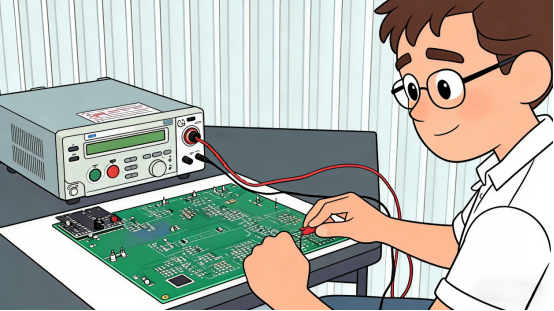
Hi-pot testing is a vital step in PCB manufacturing, ensuring that electrical products can handle high-voltage stress without compromising safety. By exposing the product to high voltage, this test assesses the strength of its insulation, preventing potential electrical failures that could lead to hazards. As electronics become more advanced and demand for reliable, high-voltage devices rises, Hi-pot testing has become essential for meeting safety standards and guaranteeing product integrity.
What is Hi-Pot Testing?
Hi-pot testing, short for "High Potential Testing," is a method used to assess the insulation strength of electrical products by applying a high voltage. During this test, a significantly higher-than-normal voltage is applied to the product's insulation to check whether it can withstand electrical stress without breaking down. The test simulates extreme operating conditions to ensure that the insulation will hold up in real-life scenarios.
For example, if you’re testing a power supply unit (PSU), you would apply a high voltage that is much higher than the normal operating voltage to make sure the internal insulation doesn’t fail under pressure. This test helps ensure that there are no risks of short circuits or electrical shocks that could arise from insulation failure.
The primary purpose of Hi-pot testing is to verify that a product’s insulation is strong enough to prevent electrical breakdown during use. This is crucial for avoiding dangerous scenarios like electric shocks or fires. Since electrical devices often operate at high voltages, any failure in the insulation can lead to catastrophic outcomes, not just damaging the device but also risking user safety.
Hi-pot testing helps prevent these issues by identifying potential weaknesses in the insulation material. It ensures that the device is safe for consumer use, meets industry standards, and passes safety certifications.
For example, consider a power strip that is used to supply power to several devices. If the insulation fails, it could expose users to the risk of electric shock. By conducting Hi-pot testing, manufacturers ensure that the insulation in the power strip can handle high voltages safely, making the product safe for everyday use.
What Are the Core Requirements of Hi-Pot Testing?
Hi-pot testing is a critical step in ensuring the safety and reliability of electrical products, but to get accurate results, certain key requirements must be met. From selecting the right test voltage to controlling leakage current, each aspect of the test plays a crucial role in confirming that a product's insulation can withstand high voltage without failing.
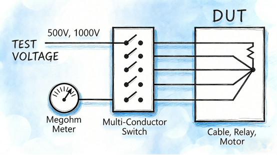
Determining the Test Voltage
The test voltage used in Hi-pot testing is crucial for evaluating the strength of a product's insulation. The correct voltage is selected based on the product's operating voltage, the type of insulation, and the application standards that the product must meet. This ensures that the test accurately simulates the conditions the product will face during real-world use.
Operating Voltage: The voltage a product is designed to handle during normal use. For example, a household electrical appliance typically operates at 110V or 220V.
Insulation Type: The material used to insulate electrical components, such as rubber, plastic, or ceramic, plays a significant role in determining the required test voltage.
Application Standards: Industry standards like UL, IEC, and GB provide guidelines for how much voltage should be applied during the test, based on the product's use and the risks involved.
Common ranges for Hi-pot test voltages are:
AC Voltage Testing: 1.5kV to 4kV is often used for testing household and industrial products.
DC Voltage Testing: For products powered by direct current, the test voltage is typically about 1.4 times the AC equivalent. This means a range of approximately 2.1kVdc to 5.6kVdc.
For example, an AC-powered device like a lamp may undergo a Hi-pot test at 2kV, while a high-voltage power supply might be tested at 4kV or more, depending on its specifications.
To improve efficiency in production environments, some manufacturers use the shortened time method. This involves applying a voltage of about 1.2 times the nominal voltage, but only for a much shorter duration, typically between 1 to 3 seconds. This method speeds up the testing process without compromising safety or accuracy.
Leakage Current Threshold
Leakage current is the amount of electrical current that flows through the insulation during the Hi-pot test. During testing, it is important to ensure that the leakage current stays within a safe limit, which indicates that the insulation is performing correctly. If the leakage current exceeds the threshold, it could suggest that the insulation is failing.
Leakage Current Limit: The threshold for leakage current is usually set between 5mA and 10mA. This is considered acceptable for most products, as it ensures that no significant electrical leakage occurs. However, for products like medical devices or sensitive equipment, the leakage current limit can be much lower, sometimes as low as 0.5mA or even lower. This is to ensure the safety of vulnerable users.
No Breakdown or Arc: In addition to keeping the leakage current under the threshold, manufacturers must ensure that no breakdown or arc formation occurs. An arc happens when the electrical current bridges the insulation, causing a spark or short circuit. If an arc occurs during Hi-pot testing, the insulation is considered to have failed, and the product will need to be redesigned or repaired.
For example, in medical devices like pacemakers, even a tiny leakage current can pose a risk to the patient. Therefore, these devices are tested with strict leakage current limits to ensure the highest safety standards are met.
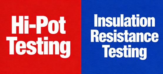
What is the Difference Between Hi-Pot Testing and Insulation Resistance Testing?
Both Hi-pot testing and insulation resistance testing are methods used to evaluate the insulation quality of electrical products, but they serve different purposes and involve different approaches.
Hi-pot Testing: High Voltage, Destructive Test
Hi-pot testing, or "High Potential Testing," applies a high voltage to the electrical product to assess whether the insulation can withstand sudden electrical stress without breaking down. This is a destructive test, meaning it checks the insulation's ability to endure extreme conditions, and if the insulation fails during the test, it is considered a failure. The goal is to simulate real-life high-voltage conditions that could occur during the product's operation, ensuring that the insulation does not allow electrical current to pass through it and cause dangerous situations like electric shock or short circuits.
For example, a power supply unit (PSU) would undergo a Hi-pot test by applying a voltage significantly higher than its normal operating voltage (e.g., 2kV for a 110V device) to see if the insulation holds up. If the insulation withstands the high voltage without any breakdown or arc, the product passes the test.
Insulation Resistance Testing: Low Voltage, Non-Destructive Test
In contrast, insulation resistance testing involves applying a much lower voltage, typically around 500Vdc, to measure the resistance of the insulation material. This is a non-destructive test, meaning that the insulation is not exposed to extreme stress. Instead, it checks for any leakage currents that might indicate weak insulation. The test calculates the electrical resistance of the insulation; if the resistance is too low, it suggests the insulation might fail under high voltage conditions, leading to safety risks.
For instance, an electrical cable might be tested with a 500Vdc voltage, and the resistance should ideally be very high (typically over 100 MΩ). A low resistance reading could indicate that the insulation is faulty or degraded, even though it may appear to work under normal conditions.
Testing Order: Insulation Resistance Test First, Then Hi-pot
Typically, the insulation resistance test is performed first, followed by the Hi-pot test. The reason for this sequence is straightforward: insulation resistance testing checks for the overall health of the insulation material, without stressing it to the point of failure. If the resistance is already too low, there's no need to perform a Hi-pot test, as the insulation is already considered weak. By performing the insulation resistance test first, manufacturers can quickly identify any potential issues with the insulation before subjecting the product to the high-voltage stress of a Hi-pot test.
For example, in a manufacturing process for power cables, the insulation resistance test would be performed initially to detect any obvious weaknesses in the insulation. If the product passes this test, the Hi-pot test would then be conducted to confirm that the insulation can withstand high voltage without breaking down.
What Impact Does Hi-Pot Testing Have on PCB Design?
When designing a PCB for high-voltage applications, ensuring the safety and reliability of the product is crucial. Hi-pot testing plays a key role in this process, as it assesses whether the insulation on the board can withstand extreme electrical stress. The results of Hi-pot testing directly impact several design decisions, from creepage distances to high-voltage trace routing.
Safety Design Considerations in the PCB Layout Stage
When designing a PCB (Printed Circuit Board), one of the most important considerations is ensuring that the board complies with safety standards for electrical products. Hi-pot testing plays a significant role in this because it evaluates whether the insulation on the board can handle high voltages without breaking down. To pass Hi-pot testing, the PCB must meet specific design requirements, particularly regarding the creepage distance and clearance.
Creepage Distance refers to the shortest path along the surface of the PCB that electricity could travel. This path should be long enough to prevent an arc from forming between conductive parts when exposed to high voltage.
Clearance refers to the shortest path through the air between two conductive parts. It ensures that there is enough physical distance to prevent electrical arcing.
For example, if the PCB is part of a high-voltage power supply, it’s crucial to ensure that the creepage distance and clearance between different parts are sufficient to withstand the voltage applied during Hi-pot testing. If these distances are too short, the PCB will fail the test, and insulation breakdown may occur, risking electrical hazards.
Grooving and Isolation Design
In some situations, simply adjusting the layout isn't enough to meet the required insulation standards. For these cases, grooving or isolation design on the PCB becomes essential. This is especially useful when you need to increase the creepage distance between high-voltage paths.
Grooving: This involves cutting isolation channels into the PCB layout to increase the distance between high-voltage components. By creating a physical gap, grooving helps to prevent electrical arcing and short circuits.
For instance, if two high-voltage traces are running too close to each other on a PCB, a groove can be cut between them to act as a barrier, significantly increasing the creepage distance and improving the insulation.
Isolation Design: In some cases, parts of the PCB can be isolated with dedicated areas or slots to ensure high-voltage components don't interfere with low-voltage circuits. This helps maintain safe operation under high-stress conditions.
By using grooving or isolation designs, PCB designers ensure that the board will pass Hi-pot testing and perform safely even under high-voltage conditions.
High-Voltage Trace Design Considerations
When designing a PCB for high-voltage applications, special care must be taken with the trace design. This refers to the layout and routing of the conductive paths on the PCB. High-voltage traces require particular attention to minimize risks like corona discharge and breakdown.
Avoid Sharp Corners: One of the most important guidelines in high-voltage trace design is avoiding sharp angles. Sharp corners in traces increase the likelihood of corona discharge—a phenomenon where electrical breakdown occurs at sharp points, causing small electrical arcs or discharges that can lead to insulation failure.
Solution: Round the corners of high-voltage traces or pads to reduce the risk of corona discharge. By using smooth curves instead of sharp turns, the risk of electric breakdown is minimized.
Increase Trace Width: In high-voltage applications, increasing the width of the traces can also help. Wider traces have better insulation properties and can handle more current without overheating.
For example, when designing a PCB for an industrial power converter, wider traces are used for high-voltage areas to ensure that the board can handle the high current without damage, ensuring compliance during Hi-pot testing.
By paying attention to the design of high-voltage traces, PCB designers reduce the risk of electrical failure and ensure that the board can pass safety tests like Hi-pot with flying colors.
How to Ensure Successful Hi-Pot Testing?
Ensuring a successful Hi-pot test is essential for the safety and reliability of electrical products. The test evaluates the insulation's ability to withstand high voltage, but its success depends on a few critical factors during the PCB manufacturing process.
Process Quality Control
Quality control during the PCB manufacturing process is crucial to ensure the product passes Hi-pot testing. The integrity of the insulation and the overall construction of the board must meet strict standards to handle high voltage without failing.
Layer-to-Layer Insulation: One of the most important factors in successful Hi-pot testing is ensuring that there are no defects in the layer-to-layer insulation. This includes checking for any gaps or inconsistencies in the material between layers that could lead to electrical breakdown during testing. For example, in multi-layer boards, poor insulation between layers could cause a short or leakage current when subjected to high voltage.
Through-hole Quality: Poor-quality via plating or through-holes can create weak points in the insulation. Any failure in these areas may result in breakdowns during Hi-pot testing. It’s crucial to ensure that the vias are properly plated and free of defects like cracks or voids that could affect electrical insulation.
Material Defects: The base material used in PCB manufacturing must be free from defects like bubbles, impurities, or irregularities. These imperfections can create weak spots in the insulation, making it more likely for the product to fail Hi-pot testing. Ensuring high-quality base materials will help the insulation perform under high voltage.
For instance, a poorly constructed PCB with improper layer-to-layer insulation or defective vias could fail the Hi-pot test by allowing current to leak through the board.
Cleanliness Control
Maintaining cleanliness during PCB manufacturing is vital to ensure that there are no contaminants that could cause leakage currents or electrical breakdowns during the Hi-pot test. Contaminants, especially in the high-voltage areas of the board, can lead to severe issues, such as ion contamination, that could result in leakage or arcing under high voltage conditions.
Surface Contamination: Residues like dust, grease, or flux left on the PCB surface can create conductive paths or attract moisture, which could lead to leakage currents during testing. This is particularly important in the high-voltage areas, where even minor contamination can cause a failure.
Ion Contamination: If ionized particles (like salts or metals) are present on the PCB, they can provide a path for current to flow, even if the insulation appears intact. This could lead to a failure during Hi-pot testing as the ions create conductive pathways that allow leakage currents to pass through the insulation.
To prevent these issues, a cleaning process should be followed to ensure that the PCB is free of any contaminants. For example, after soldering, using an ultrasonic cleaning process or other specialized cleaning methods can help remove any remaining flux or debris, ensuring the PCB's surface is clean before the Hi-pot test.
Special Material and Process Selection
For products that are subjected to extremely high voltages, it’s crucial to choose specialized materials and manufacturing processes that can provide enhanced insulation properties. These materials must be able to withstand the high-voltage stress without breaking down.
Materials with Higher Insulation Strength: For devices that are meant to operate at very high voltages, such as in power supplies or medical equipment, using materials with stronger insulation properties is necessary. For example, ceramic materials or high-performance laminates offer better insulation and higher breakdown resistance compared to standard FR4 materials.
Advanced Manufacturing Techniques: In some cases, manufacturers may need to employ special techniques to ensure high-quality insulation. These may include applying multi-layer designs to distribute high voltages more evenly or using specialized coatings that enhance the board's ability to resist electrical breakdown.
For instance, a PCB for a high-voltage power inverter might use a special polyimide film material, known for its excellent insulation properties, to prevent failures during Hi-pot testing. These materials are specifically chosen to ensure that the PCB will pass the test even under extreme voltage conditions.
Challenges and Common Issues in Hi-Pot Testing
Hi-pot testing is essential for ensuring the safety of electrical products, but it can present certain challenges. From equipment malfunctions to contamination issues, these challenges can affect the accuracy and effectiveness of the test.
Common Issues During the Testing Process
Testing Equipment Malfunctions or Voltage Instability
One of the most common issues in Hi-pot testing is testing equipment malfunction or voltage instability. Hi-pot testing relies on precise voltage levels to evaluate insulation strength, and any fluctuation in voltage or malfunction in the test equipment can lead to inaccurate results. For example, if the test equipment is not calibrated correctly or fails to maintain a stable voltage, the test could give false positives or negatives, leading to incorrect conclusions about the product's insulation.
Example: If the testing machine delivers fluctuating voltage, it could cause a product to pass or fail incorrectly, wasting time and resources on re-testing or potentially allowing defective products to pass through.
PCB Surface Contamination or Improper Handling
Another common problem is PCB surface contamination. If the PCB is not properly cleaned or if contaminants like dust, grease, or flux residue remain on the board, they can create conductive paths on the surface, leading to leakage currents or arcing during the Hi-pot test. This results in false failures or potentially dangerous breakdowns in insulation during real-world use.
Example: Even small amounts of flux residue left after soldering can create conductive paths for electricity to flow, which could lead to leakage and failure during the Hi-pot test, even if the insulation material itself is intact.
How to Address Testing Challenges
Regular Calibration of Testing Equipment
To mitigate equipment-related issues, it is crucial to regularly calibrate the testing equipment. Calibration ensures that the Hi-pot tester is delivering accurate and stable voltage levels throughout the test, preventing any false readings caused by equipment malfunction. Manufacturers should implement a routine maintenance and calibration schedule for all testing equipment to maintain reliability and precision.
Example: A company that manufactures power supplies might calibrate its Hi-pot testing equipment every month to ensure the voltage is accurately applied and to avoid test failures caused by faulty equipment.
Strict Cleaning Procedures for PCBs
To address issues of surface contamination, strict cleaning procedures must be followed at every step of the PCB manufacturing process. This includes cleaning the PCB after soldering, handling, and before testing. Advanced cleaning methods like ultrasonic cleaning or chemical cleaning can be used to ensure that no contaminants remain on the board. This helps to eliminate any potential leakage paths that could lead to failures during Hi-pot testing.
Example: A PCB assembly facility may use ultrasonic cleaning to remove flux residues and other contaminants from high-voltage areas of the board before conducting Hi-pot testing. This ensures that the surface is clean and free of any particles that could affect the test results.
Ensuring Proper Handling and Process Compliance
In addition to cleaning, it's important to ensure that the PCB is handled correctly during the manufacturing and testing processes. This means following standard operating procedures (SOPs) for PCB handling to prevent any damage or contamination. Every step, from component placement to testing, should meet established standards to ensure consistency and reliability during Hi-pot testing.
Example: If a PCB undergoes multiple assembly steps, each stage should involve a clear, documented process to handle and clean the board before it reaches the Hi-pot test. This ensures that the board will not be exposed to unnecessary contaminants or handling errors that could lead to failures.
Conclusion
Hi-pot testing is a critical process for ensuring the safety and reliability of electrical products, particularly in terms of insulation quality. By subjecting products to high-voltage stress, this test helps identify any weaknesses in insulation that could lead to dangerous situations like electric shocks or fires. Its role in product safety cannot be overstated, as it guarantees that products will perform as expected in real-world conditions and meet industry safety standards.
For companies like PCBMASTER, which specialize in providing high-quality PCBs, passing Hi-pot testing is a top priority. With years of experience in the industry, we understand the importance of rigorous testing in every stage of production. That’s why all our products undergo thorough Hi-pot testing to ensure that the insulation is flawless, and the final PCB meets the highest safety and quality standards. Our commitment to this process ensures that the PCBs we supply are reliable, durable, and safe for a wide range of applications, giving our customers peace of mind in their product development.
FAQs
Why Should Hi-Pot Testing Never Be Skipped?
Hi-pot testing is a critical step in ensuring the safety and reliability of electrical products. By applying high voltage to the insulation, Hi-pot testing verifies whether the product can withstand extreme conditions without failing. Skipping this test can result in dangerous products that pose electrical hazards, such as electric shocks or even fires. It is essential to thoroughly test the insulation before the product is put into use to guarantee its safety.
Why Does Hi-Pot Testing Require Higher Voltage?
The main reason Hi-pot testing uses high voltage is to simulate real-life operating conditions that the product will face during its use. Insulation must be able to handle more than just the typical working voltage — it must withstand momentary voltage spikes and electrical surges that can occur in daily use. By applying high voltage, the test ensures that the insulation is robust enough to avoid breakdowns over time, preventing hazardous conditions like electric shocks or fires that could arise from insulation failure.
For instance, a power supply unit that operates at 110V might be subjected to 2-3kV during Hi-pot testing, well above its normal operating voltage. This ensures that the insulation can handle occasional surges or spikes without compromising safety.
What’s the Difference Between Hi-Pot Testing and Insulation Resistance Testing?
While both tests check the quality of a product’s insulation, they serve different purposes. Insulation resistance testing involves applying a low voltage, usually around 500VDC, to measure the resistance of the insulation and determine if it is intact. This test helps identify weak insulation or degradation but does not simulate high-voltage conditions.
On the other hand, Hi-pot testing involves applying a much higher voltage to assess whether the insulation can withstand these extreme conditions without breaking down. Essentially, while insulation resistance testing looks for insulation integrity, Hi-pot testing tests the material’s strength to resist high voltage stresses.
Think of insulation resistance testing as a check for leaks in a water pipe, while Hi-pot testing is like pressure-testing the pipe to ensure it won’t burst under extreme conditions.
What Happens If the Hi-Pot Test Fails?
If a product fails Hi-pot testing, it indicates a failure in the insulation or a design flaw. A failed Hi-pot test means that the product cannot handle high-voltage stress, which could lead to short circuits, leakage currents, or electric shock hazards during actual use. To address this, the design, materials, or manufacturing process must be thoroughly inspected.
PCB Design: Ensure the design adheres to safety standards, with proper creepage distances and clearance between high-voltage components.
Materials: Check the quality of the insulation material used and ensure that it is rated for high-voltage use.
Production Process: Inspect for any flaws that may have occurred during the manufacturing process, such as poor via plating or incomplete soldering.
After identifying the problem, the design should be revised or materials replaced, and the product should undergo the Hi-pot test again to ensure it meets safety standards.
How Do Hi-Pot Testing Requirements Differ for Medical Devices?
Medical devices have stricter Hi-pot testing requirements than standard electrical products. Since these devices are used in environments where human life is at risk, ensuring patient safety is paramount. Therefore, the requirements for Hi-pot testing are much more stringent.
Leakage Current: Medical devices often require a much lower leakage current threshold than typical products. While 5mA might be acceptable for standard devices, medical equipment may require a leakage current of 0.5mA or lower, ensuring that even the smallest amount of electrical leakage does not pose a risk to patients.
Testing Conditions: The conditions under which Hi-pot testing is performed for medical devices are also more demanding. The equipment used, as well as the test parameters, may be more precisely controlled to ensure the highest level of safety.
For example, a defibrillator would undergo rigorous Hi-pot testing to ensure that its insulation can handle both high voltage and the potential for patient interaction, with extremely tight tolerance for any leakage current.
Author Bio
Hi, I'm Carol, the Overseas Marketing Manager at PCBMASTER, where I focus on expanding international markets and researching PCB and PCBA solutions. Since 2020, I've been deeply involved in helping our company collaborate with global clients, addressing their technical and production needs in the PCB and PCBA sectors. Over these years, I've gained extensive experience and developed a deeper understanding of industry trends, challenges, and technological innovations.
Outside of work, I'm passionate about writing and enjoy sharing industry insights, market developments, and practical tips through my blog. I hope my posts can help you better understand the PCB and PCBA industries and maybe even offer some valuable takeaways. Of course, if you have any thoughts or questions, feel free to leave a comment below—I'd love to hear from you and discuss further!

