


Multi-Point Grounding: A Comprehensive Guide for High-Speed Circuits
Signal integrity plays a crucial role in the performance of high-speed electronics, where even minor disruptions can lead to major issues. Traditional grounding methods often fail to meet the demands of modern circuits, particularly in high-frequency applications like 5G transceivers and advanced memory systems. Multi-point grounding provides an effective solution by ensuring more efficient return paths and minimizing noise, which is essential for maintaining performance in demanding designs.
This technique goes beyond simply adding extra ground connections. It requires careful attention to layout and execution to reduce electromagnetic interference (EMI), ground bounce, and signal reflections—key factors in preserving the clarity and reliability of high-speed signals. Understanding how multi-point grounding works reveals its importance in achieving optimal performance in today’s most complex electronic systems.
Introduction to Multi-Point Grounding
What is Multi-Point Grounding?
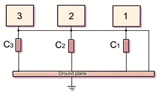
In electronic circuit design, grounding refers to the common return path for current, typically connected to the earth or a designated ground plane. Multi-point grounding differs from the traditional single-point grounding method by establishing multiple ground connections throughout the circuit. Instead of routing all return currents through a single ground point, multi-point grounding uses several strategically placed connections (vias or traces) to connect various components to the ground.
This method reduces the distance and impedance that signals must travel, resulting in faster and more reliable signal returns. It’s particularly useful in high-speed circuits, such as 5G communication systems, high-speed memory interfaces, and RF (Radio Frequency) modules, where even the smallest noise or delay can significantly impact performance.
Comparison to Traditional Single-Point Grounding:
Traditional single-point grounding connects all circuit components to a single ground reference, typically in one corner of the PCB. While this method works for simple, low-frequency circuits, it often leads to issues in high-speed designs. In single-point grounding, return currents may have to travel long paths across the board, which can increase resistance, introduce noise, and cause problems like ground bounce and signal reflections.
On the other hand, multi-point grounding allows for shorter, direct return paths. This reduces the loop area and inductance, leading to more stable and predictable signal behavior, which is essential for high-frequency applications.
Why is Multi-Point Grounding Important for Modern PCBs?
Today’s PCBs are designed to handle signals that travel at extremely high speeds, often exceeding 10 MHz, such as in 5G technology, high-definition video interfaces, and data centers. As signal frequencies increase, so do the challenges associated with maintaining clean, reliable signal paths. Multi-point grounding addresses these challenges by providing multiple short and low-impedance paths for the signal return currents.
High-Speed Circuit Requirements:
In high-speed circuits, signals are rapidly changing, meaning that return currents need to be able to flow smoothly and quickly to maintain signal integrity. When return currents encounter resistance or long, convoluted paths, it leads to signal degradation, where the signal becomes distorted or delayed. Multi-point grounding prevents this by ensuring that each component has an optimal, low-resistance path to ground, reducing the chances of signal loss or delay.
Real-life Example:
Consider a 5G transceiver, where data is transmitted at very high speeds. If multi-point grounding is not used, the return current could travel long distances across the PCB, introducing delays and signal interference. With multi-point grounding, the return current has a short, direct path to the ground, ensuring that the data remains intact and arrives at the destination without distortion.
Minimizing Ground Bounce and EMI:
One of the primary benefits of multi-point grounding is its ability to minimize ground bounce. Ground bounce occurs when there is a significant voltage difference between different parts of the ground plane, causing unwanted variations in signal voltage. This is particularly problematic for high-speed digital circuits, where even the smallest fluctuation can result in errors.
By using multi-point grounding, engineers create multiple grounding points that spread the current over a larger area, reducing the chances of ground bounce and minimizing the potential for EMI. This is particularly important in environments where different components and systems operate in close proximity to each other, such as in smartphones or data servers.
Example of EMI Mitigation:
Imagine a densely packed server motherboard that hosts various high-speed processors. If the grounding is not optimized, the high-speed signals from one part of the circuit could create interference in another part. By implementing multi-point grounding, the signals' return paths are separated and confined, reducing EMI and improving the overall performance of the motherboard.
How Does Multi-Point Grounding Work?
What are the Key Principles Behind Multi-Point Grounding?
In electronic circuit designs, signal return paths are the pathways that current takes back to the ground after completing its journey through the components. In high-frequency circuits, where signals change rapidly, return currents need to be able to move quickly and without obstruction. The faster the signal travels, the more crucial the return path becomes for maintaining signal integrity.
With multi-point grounding, these return currents flow through multiple, short, direct paths rather than one single, long route. This improves the performance of the circuit by minimizing signal distortion and delays. In traditional designs, the return current might have to travel a long distance, which increases the risk of interference, known as ground bounce, and reduces the clarity of the signal.
Ground Return Currents and Their Impact on Signal Integrity
Ground return currents are the electrical currents that flow back to the ground after passing through components in a circuit. These currents are a crucial part of signal transmission. If the return path is long or obstructed, the signal can degrade due to inductance, which is the opposition to the change in current flow. This is especially problematic for high-frequency signals, where even small disruptions can cause a loss of signal quality.
With multi-point grounding, return currents have shorter, low-resistance paths to travel, minimizing inductance and maintaining signal quality. This is especially important for high-speed circuits like 5G transceivers or DDR memory interfaces, where high-frequency signals are critical to performance.
How Does Multi-Point Grounding Optimize High-Frequency Signals?
In high-frequency circuits (typically ≥10 MHz), the impedance of the return path is crucial to maintaining signal integrity. Inductive impedance occurs when the current’s path causes magnetic fields that resist the change in current flow. This resistance can slow down the signal, distort its shape, and reduce the overall performance of the circuit. Multi-point grounding addresses this issue by creating multiple, parallel return paths, which help minimize inductive impedance.
For example, in a 5G communication module, where signals need to travel quickly and with minimal interference, each signal's return current is routed through the shortest and most direct path possible, avoiding long traces that can add unwanted resistance and inductance. This approach ensures the signal remains sharp and intact, improving data throughput and transmission reliability.
How Direct, Short Paths Improve High-Speed Signal Performance (≥10 MHz)
For high-speed circuits, the key to preserving signal integrity is minimizing the length and impedance of the return paths. The longer the return path, the more likely the signal will encounter delays, reflections, or distortion. Multi-point grounding minimizes these issues by providing shorter, more direct return paths.
For example, in a high-speed memory module, return currents are routed through vias placed directly beside signal traces. This reduces the loop area and prevents unwanted noise, which can cause data errors. By placing the vias close to the signal paths, multi-point grounding ensures that the return currents follow the shortest, least resistive route to the ground plane, preserving signal clarity at high speeds.
The Role of a Solid Ground Plane in Efficient Grounding
A ground plane is a large area of metal (usually copper) on the PCB that provides a common reference point for all return currents. It serves as the “earth” or reference for the circuit, providing a low-resistance path for return currents to flow back to. For multi-point grounding to work effectively, a solid and continuous ground plane is essential.
A fragmented or poorly connected ground plane increases the chances of ground bounce and reduces the efficiency of the return currents. A solid, uninterrupted ground plane, however, allows currents to flow smoothly and without interference, ensuring optimal signal integrity. This is especially important in high-speed designs like 10G Ethernet or RF devices, where even a small disruption in the ground can cause significant performance issues.
How Do Vias and Ground Planes Contribute to Multi-Point Grounding?
Vias are small holes in the PCB that allow signals or ground connections to pass through different layers of the board. In multi-point grounding, vias are placed close to the signal traces to ensure that the return current has the shortest possible path to the ground plane. The placement of vias is crucial because if they are too far from the signal trace, it can increase the inductive impedance, leading to slower signal returns and potential signal degradation.
In a typical server motherboard design, where multiple components communicate at high speeds, proper via placement ensures that each signal’s return current is routed efficiently back to the ground. By using multiple vias across the PCB, multi-point grounding ensures that each return current flows through the shortest, least resistive path, optimizing overall circuit performance.
Placement of Vias for Minimal Signal Return Path Length
The key to successful multi-point grounding is ensuring that vias are placed as close as possible to the signal traces they serve. The distance between the via and the trace affects the return path’s inductive impedance. If the via is too far from the signal, the return current has to travel a longer path, increasing impedance and introducing noise.
For instance, in a high-speed DDR5 memory design, vias should be placed directly next to the data lines to ensure that the return current has the shortest and lowest-resistance path to the ground plane. This setup prevents any delay or distortion in the signal and ensures that the memory operates at maximum speed and reliability.
Importance of Solid, Continuous Ground Planes
A solid ground plane is essential for multi-point grounding to function correctly. It acts as a central reference for all return currents, providing a continuous, low-resistance path for current to flow back to. If the ground plane is interrupted by traces or gaps, it increases the likelihood of signal noise and ground bounce, which can degrade performance.
In high-speed applications, like RF devices or 5G network modules, a continuous ground plane helps ensure that return currents have a clean, uninterrupted path to travel. This stability is crucial for preventing signal reflections and ensuring that high-frequency signals remain strong and reliable throughout the circuit.
Advantages of Multi-Point Grounding
What Benefits Does Multi-Point Grounding Provide for EMI Control?
Electromagnetic interference (EMI) occurs when unwanted electromagnetic signals disrupt the normal functioning of an electronic device. This is especially problematic for high-speed circuits like 5G modules, RF devices, or high-speed memory. Multi-point grounding reduces EMI by ensuring that return currents travel through multiple, shorter paths to the ground, which helps keep the overall circuit more stable.
When multiple ground paths are created, the signal return currents are distributed more evenly across the circuit, reducing the buildup of high-frequency noise. This approach significantly reduces radiated emissions, which are unwanted electromagnetic waves that can interfere with nearby circuits or systems. In fact, multi-point grounding can reduce radiated emissions by up to 20 dB, which is a substantial improvement in EMI control.
Real-Life Example:
In a 5G base station, where multiple high-speed signals are transmitted simultaneously, EMI can cause significant issues with data clarity and communication reliability. By using multi-point grounding, engineers ensure that each signal has its own efficient return path, minimizing interference and improving the overall system's reliability.
The Relationship Between Multiple Ground Paths and Lower EMI
In a PCB with single-point grounding, all the return currents flow through a single path, which can cause voltage differences across the ground plane, leading to ground bounce and unwanted EMI. When multiple ground paths are used, the return currents are spread out across the circuit, ensuring that no single path carries all the current, which reduces the risk of interference.
By spreading the return currents across multiple ground connections, multi-point grounding reduces the area over which EMI can be generated, leading to a significant reduction in the strength of radiated emissions. This is particularly important in designs where high-speed signals are involved, as faster signal transitions tend to generate more EMI. With multiple, low-resistance ground paths, the circuit is better shielded from unwanted interference.
Example in Practice:
In a server motherboard that processes large amounts of data, EMI control is crucial for maintaining system stability. Multi-point grounding ensures that each signal’s return path is optimized, reducing noise and improving the performance of the server, especially when multiple signals are transmitted at once.
How Does Multi-Point Grounding Enhance Signal Integrity?
Signal integrity refers to the quality of the electrical signals as they travel through a circuit. When return currents are not properly routed, it can lead to ground bounce and signal reflections, which degrade the signal quality and lead to errors. Multi-point grounding helps by ensuring that each signal has a short and direct return path to the ground plane, which prevents these issues from occurring.
Prevention of Ground Bounce and Reflection:
Ground bounce happens when the voltage difference between different parts of the ground plane causes signals to become distorted. In high-speed circuits, ground bounce can lead to significant data transmission errors. Multi-point grounding minimizes this by providing multiple grounding points that distribute return currents evenly. This ensures that the signal's return current doesn’t cause any unwanted fluctuations in voltage, keeping the signal clean and intact.
Signal Reflection:
Signal reflection occurs when a signal encounters impedance mismatches in the circuit, causing part of the signal to bounce back towards the source. With multi-point grounding, impedance is minimized because the return current flows through a low-resistance, consistent path, preventing reflection and ensuring that the signal reaches its destination without distortion.
Effect on Reducing Noise and Distortion in High-Speed Circuits:
In high-speed circuits, such as DDR memory modules or 10G Ethernet, signal noise can cause major performance problems. Multi-point grounding helps reduce noise by creating more efficient return paths, ensuring that signals remain strong and clear even at high frequencies.
Example:
In high-speed memory systems, like DDR5 memory, return currents must be tightly controlled to avoid delays or errors. Multi-point grounding ensures that these high-frequency signals maintain their integrity, preventing signal degradation and improving data reliability.
Why is Multi-Point Grounding Ideal for High-Density PCBs?
In high-density PCB designs, components are packed closely together, and signals must be routed across complex paths. These designs present significant challenges in ensuring proper grounding and minimizing interference. Multi-point grounding is well-suited for these applications because it ensures that return currents have multiple, short paths to the ground, reducing the impact of nearby signal interference.
Application in Large, Complex Boards (e.g., Server Motherboards):
Server motherboards, for example, handle large amounts of data and feature many high-speed components. Multi-point grounding helps maintain the integrity of signals in such complex systems. By creating multiple, evenly distributed grounding points across the board, multi-point grounding ensures that return currents don't interfere with each other, and the overall system operates efficiently without noise or data corruption.
Handling Signal Interference in Densely Packed Designs:
As circuits become denser, the likelihood of cross-talk (unwanted signal coupling between adjacent traces) and EMI increases. Multi-point grounding helps combat this by providing a stronger reference plane for signals to return to, ensuring that signals from different parts of the board do not interfere with each other. This is especially important in designs like RF transceivers, where even a small amount of interference can cause a significant drop in performance.
Real-Life Example:
In a smartphone PCB, where space is limited but high-speed components must be connected, multi-point grounding allows the design to remain compact while ensuring that signals can travel without distortion. This technique is critical in maintaining the high performance of the phone, ensuring clear communication and fast processing speeds.
Disadvantages and Challenges of Multi-Point Grounding
What Are the Potential Drawbacks of Multi-Point Grounding?
Although multi-point grounding is extremely beneficial for high-speed circuits, it may not be the best approach for low-frequency designs (≤1 MHz). For these types of circuits, using multiple grounding paths can be overkill, creating unnecessary complexity and adding no significant performance improvements.
Overkill for Low-Frequency Designs (≤1 MHz)
In low-frequency circuits, the signals are slower and less sensitive to noise, which means that a single ground connection is usually sufficient. Adding multiple grounding points can unnecessarily increase the complexity of the design without yielding significant benefits. For example, in a simple analog circuit or a low-frequency power supply, multi-point grounding may introduce unwanted complications without enhancing performance.
Example:
For a 1 MHz audio amplifier, using multi-point grounding could actually create more issues than it solves, as the return currents are slow enough that a single ground point is enough to ensure the integrity of the signal. In this case, the extra grounding points could add unnecessary costs and design challenges.
Possible Creation of Ground Loops with Multiple Paths
When using multiple ground connections, there is a risk of creating ground loops, which can lead to signal noise and interference. A ground loop occurs when there are multiple ground points with different potentials, causing current to flow between them in unexpected ways. This can result in hum, buzzing noises, or distorted signals in the system, especially in sensitive analog or RF circuits.
Example of Ground Loop:
In a home audio system, multiple components (such as a receiver, amplifier, and speakers) could form ground loops if they are all connected to different ground points, creating unwanted noise. This would disrupt the sound quality, as electrical interference travels through the ground paths and affects the signal.
How Does Multi-Point Grounding Increase PCB Complexity and Cost?
While multi-point grounding offers significant advantages in high-speed circuits, it also adds complexity to the design process. One of the main challenges is the need for additional ground planes and vias to connect various points of the PCB to the ground. These extra elements increase the number of layers and vias required, leading to a more complicated and costly design.
Need for Additional Ground Planes and Vias
To properly implement multi-point grounding, designers need to add more ground planes to ensure that multiple return paths can be provided. Each ground plane typically requires vias to connect it to the rest of the PCB. This not only complicates the design but also adds to the manufacturing time and cost. The more vias and ground planes used, the more effort is needed to ensure that they are properly placed and connected.
Example:
In a high-speed communication PCB, adding extra ground planes and vias can improve signal quality. However, each via and ground plane increases the number of steps in the design process, making the board harder to route and more expensive to manufacture. This could be a concern for mass-produced consumer electronics, where cost efficiency is crucial.
Impact on PCB Layer Count and Manufacturing Expenses
Adding extra ground planes and vias means that the PCB layer count will increase. More layers increase the cost of manufacturing the PCB, as it requires more material and more complex fabrication processes. Additionally, the increased via holes and routing requirements add to the labor and time needed for production.
Example:
Consider a server motherboard, which requires high-speed signal integrity and multiple ground planes for optimal performance. While this is necessary for the motherboard’s function, the design will result in a multi-layer PCB with added complexity, making the manufacturing process more expensive. This can be a major consideration in large-scale production runs.
What Are the Risks of Improper Via Placement in Multi-Point Grounding?
One of the critical factors in multi-point grounding is via placement. Vias are used to connect different layers of the PCB to the ground plane, ensuring that the return currents follow the shortest and most efficient paths. However, if vias are not placed correctly, they can disrupt the return path, leading to signal issues and degraded circuit performance.
How Poor Via Placement Can Lead to Broken Return Paths
When vias are incorrectly placed—either too far from the signal trace or not aligned with the ground—this can cause broken return paths. A broken return path means that the signal's return current is no longer flowing through the optimal path to the ground, causing signal distortion and increased noise. This can lead to issues such as data errors, dropped signals, or slower circuit performance.
Example:
In a DDR memory system, if the via that connects the ground plane to the signal trace is placed too far away, the return current will have to travel a longer path, introducing unwanted inductive impedance and increasing the risk of signal reflections. This can reduce the memory's reliability, causing slowdowns or failures in data access.
Impact on Signal Degradation and Performance Issues
Improper via placement can lead to performance issues such as delays, distortion, and signal reflections, which are especially problematic in high-speed circuits. This is particularly important in circuits that handle high-frequency signals, where timing is critical. A poorly placed via can cause the signal to arrive later than expected, or even cause the signal to be completely distorted, resulting in a loss of data or functionality.
Example:
In RF circuit designs, such as those used in 5G communication, proper via placement is critical for maintaining the integrity of high-frequency signals. A misplaced via could cause signal attenuation, where the signal strength is reduced, leading to poor communication performance and interference with other devices.
Best Practices for Implementing Multi-Point Grounding
How Should Ground Planes be Designed for Multi-Point Grounding?
When designing a PCB for multi-point grounding, the ground plane plays a crucial role in ensuring that return currents can flow freely and efficiently. A solid, continuous ground plane provides a common reference for all the signals, allowing them to return without encountering significant resistance or inductance.
Key Design Guidelines for Continuous, Solid Ground Planes
A continuous ground plane should cover as much of the PCB area as possible, reducing interruptions and ensuring smooth current flow. The ground plane should be kept uninterrupted by traces or other elements that could create impedance mismatches. This is important because any break in the ground plane can introduce signal reflections or noise.
Real-Life Example:
For a high-speed memory module like DDR5, a continuous ground plane helps ensure that the return currents have a stable, low-resistance path, maintaining the integrity of high-frequency signals.
Use of Multiple Connected Ground Planes in Complex Designs
In large or complex PCBs, such as those found in server motherboards or 5G base stations, multiple ground planes may be required. These planes are often connected by vias to form a single, unified ground system. Each plane may serve a different function, such as providing low impedance for high-speed signals or isolating noisy circuits from sensitive ones.
By using multiple ground planes, designers can improve signal quality and reduce interference, ensuring that return currents can follow the shortest and most direct path to the ground. However, these planes must be carefully connected to avoid creating ground loops or increasing the complexity of the PCB.
Example:
In a 5G base station, multiple ground planes may be needed to handle the numerous high-frequency signals and minimize interference. These planes must be interconnected in a way that ensures optimal signal performance while preventing cross-talk and EMI.
What Role Do Vias Play in Multi-Point Grounding?
Vias are small holes drilled through the PCB that allow electrical connections between different layers of the board. In multi-point grounding, vias are placed strategically to provide a low-resistance path for the return currents, ensuring that each signal’s return current flows smoothly back to the ground.
Proper Via Placement to Minimize Return Path Inductance
The placement of vias is critical in multi-point grounding. Vias should be placed as close as possible to the signal traces they support, minimizing the inductive impedance that could slow down or distort the return current. The farther the via is from the trace, the higher the inductance, which can lead to signal degradation and loss of data integrity.
For instance, in high-speed circuits like 10G Ethernet, placing vias directly next to the signal traces ensures that the return current can flow efficiently, reducing noise and maintaining signal clarity.
Example:
In high-speed digital circuits (e.g., DDR memory), improperly placed vias can increase signal delay and noise, causing performance issues. By placing vias close to the signal traces, designers can reduce signal degradation and improve overall performance.
Via Types and Selection Criteria for Optimal Performance
There are different types of vias—through-hole vias, blind vias, and buried vias—each with different applications. For multi-point grounding, through-hole vias are often the most suitable as they connect the top layer directly to the bottom layer, providing a direct path for return currents. Blind vias and buried vias are used in more complex designs with multiple layers, but their placement must still ensure minimal inductive impedance.
Example:
In a server motherboard, where multiple layers are needed, the designer might use blind or buried vias to optimize the layout and ensure that all signal traces are properly grounded, reducing interference and signal loss.
How Can Designers Avoid Common Pitfalls in Multi-Point Grounding?
Despite its advantages, multi-point grounding can introduce complications if not implemented correctly. Common issues include ground loops, noise, and improper via placement. By following best practices, designers can avoid these problems and ensure that the grounding system works as intended.
Techniques to Prevent Ground Loops and Noise
Ground loops occur when multiple ground points are at different electrical potentials, causing unwanted current flow between them. To prevent ground loops, it’s essential to carefully design the PCB’s grounding system, ensuring that all ground points are connected properly and that there are no significant voltage differences between them. Additionally, placing decoupling capacitors near sensitive components can help reduce noise and smooth out voltage fluctuations.
Example:
In a high-performance audio system, ground loops can lead to unwanted hum or noise. By using multi-point grounding and ensuring proper connections between the ground points, designers can eliminate these issues and achieve clear, noise-free audio performance.
Importance of Ensuring Low Impedance Between Signal Traces and Ground
To maintain signal integrity, it’s crucial to keep impedance low between signal traces and the ground plane. High impedance can lead to signal reflections and noise. Designers should route signal traces as close as possible to the ground plane and avoid unnecessary gaps. This helps to ensure that the return current flows smoothly and without disruption.
Example:
In high-speed digital communication systems like 5G or HD video interfaces, maintaining low impedance between the signal traces and the ground is essential. Any impedance mismatch can cause signal degradation, which can result in data loss or communication failure.
Multi-Point Grounding in Specific Applications
Why is Multi-Point Grounding Crucial for High-Speed Digital Circuits?
In high-speed digital circuits, data transmission rates are extremely fast, with signals frequently switching between high and low states. For example, DDR5 memory operates at speeds exceeding 5,000 MT/s, and 10G Ethernet handles data at 10 gigabits per second. At these high speeds, signal integrity is critical, and any noise or delay can lead to data loss, errors, or slower performance.
Multi-point grounding helps by providing multiple low-resistance paths for return currents. These shorter paths reduce inductive impedance, which is a major source of signal degradation in high-speed circuits. By ensuring that each signal’s return current flows through the shortest, most direct path to the ground, multi-point grounding minimizes delays and signal reflections, keeping the data transmission clear and fast.
Example:
In a DDR5 memory module, the signal paths carrying data must return to the ground quickly and without distortion. Using multi-point grounding ensures that the return currents follow direct paths, reducing the chance of signal jitter and improving overall memory performance. This is especially important in high-performance computing systems where speed and reliability are critical.
Impact on High-Speed Data Transmission (e.g., DDR5, 10G Ethernet)
For circuits like DDR5 memory and 10G Ethernet, where high-speed data must be transmitted with minimal delays, multi-point grounding plays a crucial role. These circuits rely on high-frequency signals that are susceptible to distortions caused by impedance mismatches, noise, and signal reflections. By using multi-point grounding, the grounding system is optimized for the specific needs of high-speed digital transmission, ensuring that return currents flow smoothly without creating noise or interfering with the signals. This leads to faster, more reliable data transmission with fewer errors and delays.
Example:
In a 10G Ethernet system, data packets must be transmitted across the network with minimal loss. Multi-point grounding ensures that the return currents from the high-speed transmission lines are efficiently routed to the ground, preventing delays and signal loss.
How It Improves Performance in High-Frequency Digital Designs
High-frequency digital designs require grounding systems that can handle the rapid switching of signals without introducing noise or causing delays. Multi-point grounding works by reducing loop area and inductive impedance between signal traces and ground. The shorter and more direct the return path, the less likely it is that electromagnetic interference (EMI) will distort the signal. This is crucial for maintaining signal integrity in high-speed digital designs, as even small disturbances can cause significant performance issues.
Example:
In a high-speed processor or FPGA, multi-point grounding ensures that each signal’s return current follows a path with minimal impedance, allowing for faster clock speeds and reducing errors in data transmission.
How Does Multi-Point Grounding Benefit RF and 5G Circuits?
In RF circuits and 5G systems, signals operate at much higher frequencies than typical digital circuits, often in the GHz range. These high-frequency signals are particularly sensitive to electromagnetic interference (EMI) and signal degradation. Multi-point grounding is critical for these applications because it helps to maintain the quality of the transmitted signal by providing multiple, efficient paths for the return currents. This ensures that the signal remains strong and clear, preventing noise and ensuring proper transmission between components.
Specific Advantages for RF and 5G Transceiver Boards
In RF transceivers and 5G communication systems, maintaining the integrity of high-frequency signals is essential for reliable communication. Multi-point grounding provides the following advantages:
Reduces EMI: By creating multiple, direct return paths, multi-point grounding minimizes the chances of noise interfering with the RF signal, improving signal-to-noise ratio (SNR) and enhancing communication quality.
Prevents Ground Bounce: Multi-point grounding minimizes the voltage differences across the ground plane, reducing the risk of ground bounce—a common issue in high-speed circuits where fluctuations in the ground potential cause signal distortion.
Enhances Performance: As 5G systems rely on high-speed, low-latency data transmission, multi-point grounding ensures the signal integrity is maintained, preventing delays and ensuring faster data rates.
Example:
In a 5G base station, the RF signals must be transmitted with minimal delay and distortion to ensure high-speed, reliable communication. Multi-point grounding helps maintain the signal integrity by reducing EMI and ensuring that the return currents flow efficiently back to the ground.
Managing High-Frequency Signals in Compact, High-Speed Modules
5G and RF transceiver boards are often compact, with many components packed into a small area. The challenge in these designs is to ensure that the high-frequency signals remain clear and free from distortion, despite the dense layout. Multi-point grounding is particularly beneficial in these situations because it helps maintain low-impedance return paths, even in tight spaces.
By placing vias and creating multiple ground connections near the signal traces, designers can ensure that the return currents have the shortest and most efficient path back to the ground, reducing signal loss and ensuring reliable performance.
Example:
In a 5G smartphone or small RF transceiver, multi-point grounding is used to ensure that even in a compact, high-density layout, the RF signals can be transmitted without significant interference or degradation. This allows the device to maintain high-speed communication even in challenging environments.
Conclusion
Engineers should seriously consider multi-point grounding for high-speed designs because it directly impacts the performance and reliability of modern PCBs. By creating multiple direct paths to the ground, multi-point grounding minimizes signal degradation, reduces electromagnetic interference (EMI), and ensures the integrity of high-frequency signals. This is crucial in applications like DDR5 memory, 10G Ethernet, and 5G transceivers, where even small distortions can lead to significant performance issues. Proper grounding not only enhances signal quality but also prevents common problems like ground bounce and signal reflections, ensuring smooth data transmission and faster processing speeds.
In the rapidly evolving world of high-speed electronics, multi-point grounding plays an essential role in achieving the high performance and stability required by cutting-edge devices. With the right grounding system, engineers can ensure their designs are optimized for both functionality and efficiency. Whether designing RF circuits or high-speed digital systems, multi-point grounding is a key strategy for maintaining top-tier performance and minimizing errors. If you have any further questions or need expert advice on PCB design, feel free to reach out to PCBMASTER, a seasoned PCB supplier ready to provide professional solutions and insights.
FAQ: Common Questions About Multi-Point Grounding
How Does Multi-Point Grounding Improve Signal Integrity in High-Speed Circuits?
Multi-point grounding enhances signal integrity by ensuring that return currents follow short, direct paths to the ground. In high-speed circuits, such as those used in DDR5 memory or 10G Ethernet, long return paths can introduce unwanted inductive impedance, causing signal degradation and delays. By placing ground connections near signal traces and ensuring multiple, low-resistance paths, multi-point grounding minimizes these issues. The result is reduced noise, better signal-to-noise ratio (SNR), and improved data transmission performance.
Can Multi-Point Grounding Be Used in Low-Frequency Circuits?
Multi-point grounding is typically not necessary or beneficial for low-frequency circuits operating at or below 1 MHz. At these frequencies, signal integrity is less susceptible to issues like inductive impedance and ground bounce, which are the main concerns in high-speed circuits. For low-frequency designs, a single ground connection is usually sufficient, and adding multiple paths can introduce unwanted complexity, cost, and the potential for ground loops, without improving performance.
What are the Key Challenges When Implementing Multi-Point Grounding?
The main challenges of implementing multi-point grounding are cost and complexity. Multi-point grounding typically requires additional ground planes, vias, and layers in the PCB design, which increases both the design time and the manufacturing cost. Moreover, via placement must be done carefully to ensure proper return current paths, which can be difficult in complex, high-density designs. These challenges make multi-point grounding more suitable for high-speed and high-performance applications but less practical for simpler, low-frequency designs.
How Can I Minimize Ground Loops in Multi-Point Grounding Designs?
To minimize ground loops, it is crucial to carefully design the grounding system. Here are some tips:
Control via placement: Ensure that vias are placed close to the signal traces they are supporting, minimizing impedance and ensuring that return currents follow the shortest path.
Continuous ground planes: Avoid breaks in the ground plane and ensure that all ground points are connected properly. This reduces the risk of ground loops by keeping the potential difference across the ground plane uniform.
Use of decoupling capacitors: These capacitors can help filter out noise and stabilize voltage fluctuations, further reducing the risk of ground loops.
What is the Impact of Multi-Point Grounding on PCB Manufacturing Costs?
Multi-point grounding can increase PCB manufacturing costs due to the need for additional ground planes, vias, and layers. Each additional layer adds material and fabrication time, while vias increase the number of drilling steps in the PCB production process. These factors lead to higher costs compared to simpler designs with fewer layers. However, for high-speed applications where performance is critical, these additional costs may be justified by the improvements in signal integrity, reduced EMI, and overall circuit reliability.
Author Bio
Hi, I'm Carol, the Overseas Marketing Manager at PCBMASTER, where I focus on expanding international markets and researching PCB and PCBA solutions. Since 2020, I've been deeply involved in helping our company collaborate with global clients, addressing their technical and production needs in the PCB and PCBA sectors. Over these years, I've gained extensive experience and developed a deeper understanding of industry trends, challenges, and technological innovations.
Outside of work, I'm passionate about writing and enjoy sharing industry insights, market developments, and practical tips through my blog. I hope my posts can help you better understand the PCB and PCBA industries and maybe even offer some valuable takeaways. Of course, if you have any thoughts or questions, feel free to leave a comment below—I'd love to hear from you and discuss further!

