


Rigid-Flex PCBs: Key Structure and Design Requirements for Reliable Electronics
Rigid-flex PCBs are a vital innovation in modern electronics, merging the flexibility of flexible circuits with the durability of rigid boards. This unique combination allows engineers to design compact, reliable, and versatile devices, from smartphones to medical equipment. As the demand for smaller, more efficient electronics grows, understanding the structural intricacies and design principles behind rigid-flex PCBs becomes crucial. Whether you're developing the next cutting-edge wearable or optimizing automotive electronics, mastering these design elements ensures both performance and durability. Let’s explore how the structure and design of rigid-flex PCBs create the foundation for these advanced technologies.
Structure of Rigid-Flex PCBs
Basic Overview of Rigid-Flex PCBs
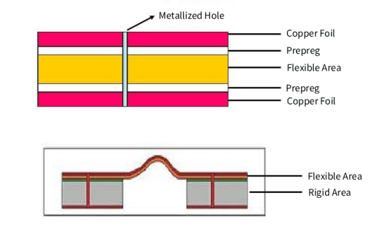
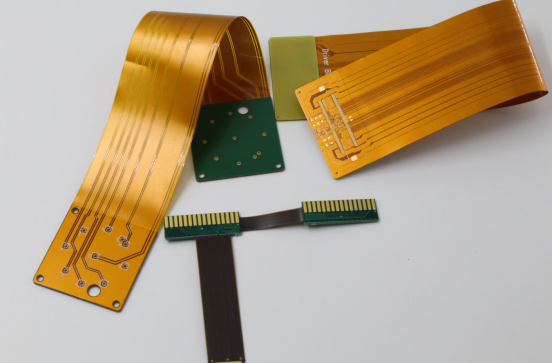
Rigid-flex PCBs combine two types of circuits: rigid and flexible. The rigid area provides strength and support, while the flexible area allows the circuit to bend, making it ideal for compact and complex designs. This combination is used in a variety of applications where space and durability are key, such as smartphones, wearables, and medical devices.
The rigid zones are typically made from sturdy materials, similar to traditional circuit boards, and are designed to maintain their shape. The flexible zones, on the other hand, use flexible materials like polyimide that allow the circuit to twist and bend. These areas are often used to connect components in tight spaces or in devices that need to flex during use, such as foldable phones or robotic systems.
Common Types of Rigid-Flex PCBs
There are two main types of rigid-flex PCBs commonly used in electronics:
Type 1: Rigid-Flex Combination Board
This type of board consists of both rigid and flexible sections that are bonded together, but without the use of plated-through holes (PTH). In this design, the rigid and flexible areas are connected at the surface level, often using adhesives or special bonding processes. This design is typically simpler and is used for applications where minimal interconnection between layers is required.
Structure: Rigid boards and flexible circuits are joined together through adhesive bonding.
Advantages: Less complex, lower cost, ideal for simpler designs that do not require extensive layering.
Example: Early mobile phones used Type 1 rigid-flex boards to connect buttons and screens with the main board.
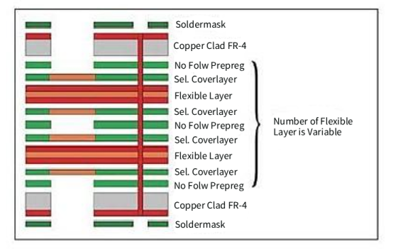
Type 2: Rigid-Flex Multi-layer Board
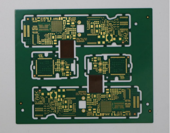
Rigid-flex multi-layer boards have multiple layers of both rigid and flexible sections, with PTH used for more advanced electrical connections. This type allows for more complex designs with multiple circuit layers, providing more flexibility in routing and higher component density. Multi-layer boards are typically used for high-performance applications that require increased reliability and space efficiency.
Structure: Multiple layers of rigid and flexible circuits, interconnected with plated holes.
Advantages: Higher performance, suitable for complex devices where many connections and layers are required.
Example: Wearable devices like smart glasses often use rigid-flex multi-layer boards, which need complex, compact connections and high-density components.
Key Structural Elements
Rigid-flex PCBs are unique because they combine both rigid and flexible sections in one board. Here are the key elements of their structure:
Rigid and Flexible Areas
A rigid-flex PCB will always contain at least one rigid area and one flexible area. The rigid sections are usually used for components that need a solid, stable base, such as processors or connectors. The flexible sections are used for parts of the circuit that must bend or be folded, like connectors to sensors or actuators.
Rigid Area: Solid, used for durable components that should not move.
Flexible Area: Can bend or fold, used for connections that need to move with the device.
Electrical Connections Between Rigid and Flexible Areas
In rigid-flex boards, the rigid and flexible sections are electrically connected through conductive paths. These connections can be made by through-holes (PTH) or surface-mount technology (SMT), depending on the complexity of the design. In Type 2 boards, these connections may also involve via holes that pass through multiple layers, allowing for more complex and high-density connections.
PTH: Used for connecting different layers by passing through the entire board.
SMT: Used for attaching components to the surface of the PCB, common in flexible areas.
For example, in a foldable phone, the rigid parts of the PCB might hold the screen and main processor, while the flexible areas connect the display to the motherboard and allow the device to fold without damaging the circuits.
Design Requirements for Rigid-Flex PCBs
Design of Flex Circuit Lines
When designing the flexible areas of a rigid-flex PCB, it is crucial to ensure that the circuit lines are both reliable and flexible. The flex circuit lines need to be designed in a way that avoids sudden changes in width or direction, as these could create weak points that may break or cause electrical failure over time.
Smooth Transitions: To avoid electrical issues and physical stress, the design should incorporate smooth, gradual transitions for circuit lines. Sharp angles or sudden changes in the width of the line can lead to stress concentrations and increase the risk of failure. A tear-drop shape is often used to smoothly connect wide and narrow traces.
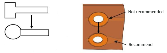
Pad Design: The pads where components are soldered must also be designed for optimal performance. The pad size and shape should be large enough to accommodate soldering, but not so large that they waste space or cause unnecessary stress on the flex material. A round shape is often preferred for pads to reduce stress concentration around the edges.
Dimensional and Material Design
The design of a rigid-flex PCB must also consider both the dimensions and the materials used. Proper material choice ensures flexibility and durability, while careful dimensional planning avoids design flaws and improves performance.
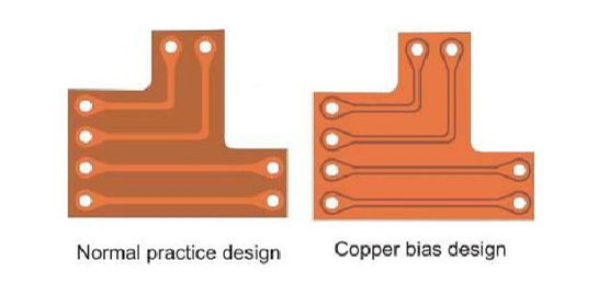
Copper Foil Design and Waste Area Considerations: The copper foil used in the flexible section must be thin and flexible, but also conductive enough to support the electrical current. The design should optimize the use of copper and minimize waste areas. In regions where the circuit does not need to conduct electricity, these areas should be kept as small as possible to reduce material cost and waste.
Coverlay Window Design: The coverlay is a protective layer that covers the flexible section of the PCB, protecting it from environmental factors and mechanical stress. The window in the coverlay (the area that is cut out for the flexible circuit) should be designed to improve alignment accuracy and adhesive flow. The cutout should be slightly larger than the circuit to allow the adhesive to bond securely and avoid air pockets that might cause issues during use.
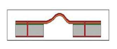
Design of Rigid-Flex Transition Zone
The transition zone between the rigid and flexible areas of the PCB is one of the most critical parts of the design. This is where the circuit moves from a rigid structure to a flexible one, and it needs to be designed carefully to avoid physical and electrical failures.
Smooth Transitions: The circuit lines in the transition zone should maintain a smooth, gradual curve to avoid sharp bends or stress concentrations. This prevents breakage or poor electrical connections that can occur in areas with tight, abrupt bends. Round edges and wide radii are preferred in the transition zones for both the lines and the copper traces.
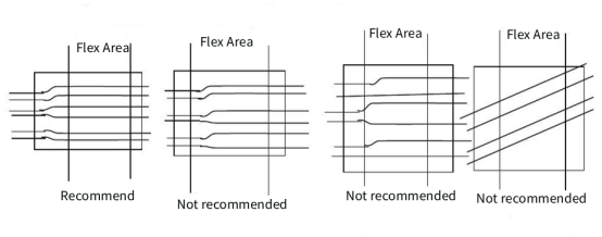
Wire Distribution in the Bending Area: In flexible areas that will experience bending, the distribution of the wires needs to be uniform and optimized. The width of the wires should be maximized in the bending zone to ensure the circuit can handle stress without failure. The more evenly the wires are distributed, the less likely the PCB is to break under pressure.
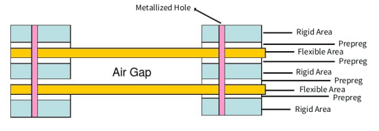
Air-Gap and Protective Copper Wire Design
Designing the air-gap and placing protective copper wires in the flexible areas are crucial to ensure the longevity and reliability of the PCB, especially in areas that experience bending.
Protective Copper Wire Placement and Connection Requirements: In bending zones, protective copper wires are added alongside the main conductive traces to provide extra strength and reduce the risk of breakage. These protective wires should be placed along the edges or within the bend to help maintain the integrity of the circuit. They can also act as a backup if the main circuit lines break or fail.
Air-Gap Design and Challenges: The air-gap refers to the space between the conductive traces in the flexible area that should be free of any components or conductive material. This gap is crucial to avoid short circuits when the PCB is bent or folded. Designing the correct air-gap size is essential, as too little space can lead to unwanted connections, while too much space may reduce the board's efficiency and compactness.
Challenges in Rigid-Flex PCB Design
Design Complexity
Designing a rigid-flex PCB comes with unique electrical and mechanical challenges, especially when integrating both rigid and flexible sections. These challenges require careful planning to ensure the final product works as intended, while also maintaining high performance and durability.
Electrical and Mechanical Challenges in Combining Flexible and Rigid Areas
When combining rigid and flexible regions on a PCB, the electrical connections between these two sections can be complex. The materials used in the rigid sections (like FR4) differ from those in the flexible areas (like polyimide). As a result, the thermal expansion rates of these materials may vary, which can cause stress at the connection points. These stresses could lead to cracking or malfunction over time if not properly designed.
High-Density Connections and Limited Space
Another design challenge in rigid-flex PCBs is the need for high-density connections in a limited space. As devices get smaller, the available space for placing components becomes tighter. Designing a rigid-flex PCB that can handle many connections in a small area requires careful planning of the trace routing, component placement, and layer stacking. Improper planning could result in crowded designs, leading to signal interference, poor performance, or even failure.
Manufacturing Process Limitations
Manufacturing a rigid-flex PCB involves several precision processes, and any deviation from the required standards can result in defective products. There are specific limitations in the lamination and metalization processes that must be carefully managed to ensure the quality of the final product.
Precision Control in Lamination and Metallization
The lamination process involves bonding the different layers of the PCB together. In rigid-flex PCBs, this process is more complex because it involves both rigid and flexible layers. Ensuring that the adhesives are evenly applied and that the layers are correctly aligned is critical. Additionally, metalization, or the process of adding metal to the holes for electrical connections, must be done with high precision. Poor metallization can lead to weak or faulty electrical connections, affecting the PCB's performance.
High Precision Requirements for Materials and Dimensions
Another manufacturing limitation in rigid-flex PCBs is the high precision required for the materials and dimensions. The materials used in rigid-flex designs need to have consistent thicknesses and properties. Even a small variation in the material thickness or size can affect the performance and reliability of the PCB. Additionally, because of the small sizes and compact designs of modern electronic devices, the PCB must be manufactured with extremely tight tolerances. Deviations in dimensions can result in poor fits, weak connections, or failure to meet quality standards.
Conclusion
Designing rigid-flex PCBs involves addressing key challenges, such as integrating rigid and flexible sections, optimizing high-density connections, and ensuring smooth electrical transitions. These challenges require precise planning and innovative solutions to ensure performance, durability, and reliability in compact devices.
For fast, reliable, and high-quality rigid-flex PCBs, look no further than PCBMASTER. Offering 7-day delivery for 10-layer rigid-flex boards, PCBMASTER provides quick turnaround times, from 6 to 20 layers. Whether you need standard designs or advanced HDI technology, PCBMASTER uses top-tier materials from trusted brands like DuPont, Panasonic, and Shinko, and can even accommodate designs as small as 0.8mm in length.
Partner with PCBMASTER for all your rigid-flex PCB needs and experience speed, precision, and excellence.
FAQs
Why should sharp right-angle bends be avoided in rigid-flex PCBs?
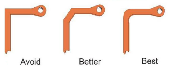
In rigid-flex PCBs, sharp right-angle bends should be avoided because they create stress concentrations in the circuit, which can lead to cracks or failures over time, especially in the flexible areas. These sharp angles cause mechanical stress that can weaken the circuit's structure, particularly when the PCB undergoes bending or movement. To reduce the risk of failure, smooth transitions and rounded corners are used instead of sharp angles. This ensures a more uniform stress distribution, increasing the durability of the PCB during its lifecycle.
How can pad design be optimized in rigid-flex PCBs?
In rigid-flex PCB design, optimizing pad design is crucial for ensuring strong and reliable electrical connections. To achieve this:
Pad Size: The pads should be large enough to accommodate the required components and provide adequate surface area for soldering. However, they should not be too large, as this can waste space and potentially create mechanical stress.
Pad Shape: Round pads are typically preferred over square or rectangular ones to reduce the risk of stress concentration at the edges. Additionally, pad-to-trace transition should be gradual, ensuring smooth and reliable solder joints.
Avoiding Sharp Corners: The transition between the pad and the trace should be rounded, not sharp, to prevent potential weak points that may fail during bending or thermal cycling.
Properly optimized pads lead to stronger electrical connections and improve the PCB's overall durability, especially in flexible areas where movement is expected.
How should trace width changes be handled in flexible areas of rigid-flex PCBs?
In the flexible areas of rigid-flex PCBs, trace width changes should be handled with care to avoid electrical issues or mechanical failure. Here are key design considerations:
Smooth Transitions: Sudden changes in trace width should be avoided, as they can cause stress concentrations and affect the current-carrying capability. Instead, use tear-drop shapes or gradual transitions to ensure smooth changes in width.
Consistent Trace Width: Maintaining a consistent trace width throughout the flexible section is essential for reducing electrical resistance and improving signal integrity. This is particularly important in high-frequency applications.
Optimizing for Flexibility: Trace width should also be optimized for flexibility. Narrow traces are more prone to breaking during bending, so using slightly wider traces in the flexible zones can help distribute stress more evenly.
By following these principles, the flexibility of the PCB is maintained without sacrificing electrical performance.
What are the key requirements for designing the transition zone between rigid and flexible sections of a rigid-flex PCB?
The transition zone between rigid and flexible areas in a rigid-flex PCB is one of the most critical areas to design, as it is subjected to both electrical and mechanical stresses. Key design considerations include:
Smooth Transitions: The lines and traces should have rounded edges and gradual curves to ensure uniform stress distribution. Sharp angles should be avoided, as they can cause stress points that may lead to mechanical failure.
Uniform Trace Distribution: The traces in the transition zone should be evenly distributed to avoid any imbalance that could cause weak points. The wider the traces in the transition area, the better the distribution of stress and current.
Adequate Stiffness: The rigid-flex transition zone should have a balance of rigidity and flexibility to prevent flexing from damaging the PCB. The transition area should not be too rigid or too flexible; it must support the PCB during bending while maintaining electrical integrity.
Properly designing this transition area ensures that the PCB performs reliably, even when bent or flexed repeatedly.
What are the air-gap requirements in rigid-flex PCB design?
The air-gap in rigid-flex PCB design refers to the space between conductive layers, particularly in flexible areas. The key requirements for air-gap design are:
Sufficient Air-Gap: There should be enough space between the conductors to prevent short circuits when the PCB is bent. Too little air-gap could cause the layers to touch, leading to electrical failure. The air-gap size should be designed carefully to accommodate the movement of the flexible PCB without causing electrical faults.
Minimizing Mechanical Interference: In areas of the PCB that experience bending, the air-gap should be sized to avoid interference from adjacent conductive layers. If the gap is too narrow, it could lead to mechanical failure due to the stress applied during bending.
Space Efficiency: While it's important to have an adequate air-gap for reliability, it should not be excessively large. A well-designed air-gap ensures that the rigid-flex PCB is both efficient and reliable without compromising the overall design.
The air-gap ensures the safety and performance of the PCB, especially in highly flexible or dynamic environments, such as wearable devices and foldable electronics.
Author Bio
Hi, I'm Carol, the Overseas Marketing Manager at PCBMASTER, where I focus on expanding international markets and researching PCB and PCBA solutions. Since 2020, I've been deeply involved in helping our company collaborate with global clients, addressing their technical and production needs in the PCB and PCBA sectors. Over these years, I've gained extensive experience and developed a deeper understanding of industry trends, challenges, and technological innovations.
Outside of work, I'm passionate about writing and enjoy sharing industry insights, market developments, and practical tips through my blog. I hope my posts can help you better understand the PCB and PCBA industries and maybe even offer some valuable takeaways. Of course, if you have any thoughts or questions, feel free to leave a comment below—I'd love to hear from you and discuss further!

