


The Importance of EMC Design in Printed Circuit Boards (PCBs)
Every day, we use countless electronic devices, often without considering the invisible forces at play around them. Yet, when these devices start to interfere with each other—like a phone call dropping near a microwave—it's a clear sign that something's gone wrong. At the heart of this issue lies a critical but often overlooked aspect of electronics design: Electromagnetic Compatibility (EMC). It’s what ensures that our devices not only function properly in isolation but also coexist peacefully in an increasingly connected world. Without it, even the most advanced gadgets can become unreliable, unsafe, or even hazardous. Understanding EMC design in PCBs (Printed Circuit Boards) is essential for creating electronics that work seamlessly and safely, both for consumers and manufacturers alike.
Introduction to EMC Design in PCBs
What is Electromagnetic Compatibility (EMC)?
Definition and Role in Electronics:
Electromagnetic Compatibility (EMC) refers to the ability of electronic devices to function without causing interference to other devices and without being affected by interference from other devices. In simpler terms, it ensures that a device works properly while interacting with the electromagnetic "environment" around it. Every electronic device, from your phone to medical equipment, generates electromagnetic signals. If not properly managed, these signals can disrupt other devices, leading to malfunctions or even safety hazards. EMC design ensures that these devices can "coexist" without interference, enabling them to operate smoothly.
Importance of EMC in Ensuring Device Functionality and Safety:
EMC design plays a key role in ensuring the proper functioning and safety of electronic devices. For example, a well-designed EMC system prevents a microwave from interfering with your Wi-Fi signal, or a mobile phone from causing noise in an audio system. In critical areas, like healthcare, poor EMC design can be dangerous—imagine a medical monitor malfunctioning due to electromagnetic interference (EMI), which could endanger a patient’s life. Therefore, EMC is not just about performance—it’s also about safety, ensuring devices work reliably in all environments, from homes to hospitals.
EMC Standards and Compliance
Global EMC regulations are in place to ensure that electronic devices do not emit excessive electromagnetic interference (EMI) and are not vulnerable to external EMI. These regulations help maintain the safety, functionality, and reliability of devices across different regions. Some of the key EMC standards include:
FCC (Federal Communications Commission): In the U.S., the FCC sets strict rules for electromagnetic emissions from electronic devices. Devices must meet these standards before they can be sold in the U.S. The FCC tests devices for both radiated emissions (EMI emitted into the air) and conducted emissions (EMI traveling through power lines or cables).
CE (Conformité Européenne): In Europe, products must carry the CE mark to show they meet EMC requirements. This mark ensures that the device complies with European Union regulations on electromagnetic interference and safety, allowing it to be sold in EU countries.
C-Tick: In Australia, the C-Tick mark indicates that a product complies with Australian EMC regulations. Like the FCC and CE standards, it ensures that the device does not emit excessive EMI or suffer from external interference.
These standards aim to prevent disruptions in the operation of electronic devices and protect consumers from potentially harmful interference.
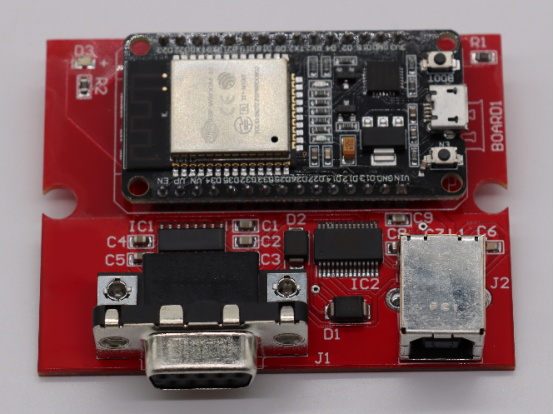
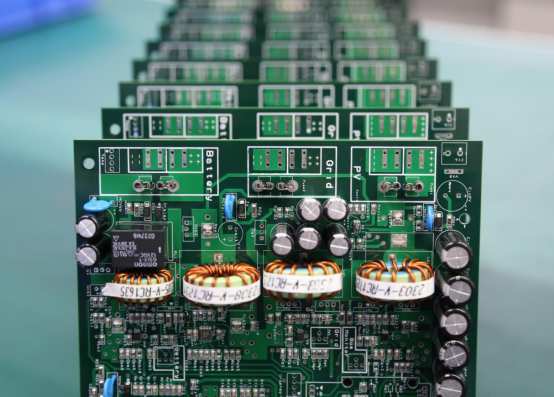
Key Components of EMC Design in PCB
Shielding in PCB Design
Purpose and Importance of Shielding in Preventing EMI:
Shielding is a crucial technique in Electromagnetic Compatibility (EMC) design, primarily aimed at preventing electromagnetic interference (EMI) from entering or leaving a device. EMI can disrupt the normal operation of electronic devices, leading to problems like dropped signals, malfunctioning components, or poor performance. Shielding acts as a protective barrier around sensitive areas of the PCB, blocking unwanted electromagnetic waves from entering the device and preventing the device’s signals from leaking out and interfering with nearby electronics. Essentially, shielding ensures that the device performs as intended without disrupting other devices in its vicinity.
Types of Shielding Materials and Techniques:
There are several shielding materials and techniques used in PCB design, each offering different levels of protection:
Metal Enclosures: A metal casing or enclosure is commonly used to shield the entire device. The metal acts as a barrier that blocks EMI from entering or escaping.
Shielding Covers: These are used to cover specific sensitive components on the PCB, like microchips or oscillators. They help minimize the impact of external EMI on these critical areas.
Conductive Coatings: Some PCBs use special conductive coatings, such as conductive paint or ink, to create a protective layer on the surface of the PCB.
Shielded Cables: In some cases, the cables connecting the device’s components are also shielded using metal braiding or foil to prevent EMI from traveling through the cables.
A good shielding design ensures that the device is less susceptible to interference, both from external sources and from the device's own internal signals.
Grounding: A Crucial EMC Design Technique
Explanation of Grounding and Its Impact on Reducing Interference:
Grounding is another critical EMC design technique that helps reduce interference. It provides a safe path for excess electrical energy to flow away from the device, preventing it from affecting the device's performance or interfering with other devices. Grounding helps stabilize the operation of the device by creating a low-resistance path for electrical current to return to the ground. Without proper grounding, electrical noise can build up, causing erratic behavior, overheating, or even device failure.
In PCB design, grounding is essential for preventing unwanted voltage differences between different components on the board, which could lead to signal interference. A solid grounding system minimizes the effects of EMI, ensuring that the device functions consistently and reliably.
Best Practices for Grounding in PCB Layouts:
Proper grounding is critical for effective EMC performance. Here are some best practices:
Single Ground Plane: Using a single ground plane on the PCB helps ensure that all components are connected to a common reference point, reducing the risk of electrical noise.
Short Ground Paths: Keeping the ground paths short and direct minimizes resistance and the potential for interference. The shorter the path, the less noise and resistance there will be.
Avoiding Ground Loops: Ground loops occur when multiple ground points are connected in a way that creates a circular path for the electrical current, which can lead to unwanted interference. To prevent this, ensure that the ground plane is continuous and not split into separate sections.
Connecting Shielding to Ground: Any shielding used in the device should be properly connected to the ground plane at only one point to prevent ground loops and ensure effective EMI protection.
By following these grounding best practices, you can reduce EMI and improve the overall reliability of the device.
Optimized PCB Layout for EMC
Importance of Strategic Component Placement and Trace Routing:
A well-designed PCB layout is one of the most effective ways to minimize EMI. The placement of components on the PCB and the routing of traces play a major role in how well the device will resist interference. For example, placing high-frequency components, like oscillators or microprocessors, away from sensitive analog areas can prevent unwanted noise from affecting critical signals. Similarly, careful routing of traces can minimize the loop area and reduce the likelihood of EMI being generated.
Strategic placement and routing ensure that signals do not mix in ways that could create interference, leading to better performance and fewer malfunctions.
Layout Practices that Minimize EMI:
Here are some layout practices that help minimize EMI and improve EMC performance:
Solid Return Reference Plane: A solid, unbroken ground plane provides a stable reference for all signals on the PCB. This reduces the chances of signal interference and ensures that the signals travel along the shortest, most reliable paths.
Grouping I/O Ports Together: Grouping input/output (I/O) ports on one side of the PCB minimizes voltage differences between different sections of the board, reducing the likelihood of EMI.
Separating Power and Signal Traces: Separating power traces from signal traces helps to avoid noise coupling from high-current paths into sensitive signal lines.
Minimizing Trace Lengths: Shorter traces help reduce the surface area available for radiating EMI. It also reduces the resistance and capacitance between components, improving signal integrity.
Using Grounded Vias: Grounded vias (holes in the PCB that connect different layers) can be used to connect the ground plane to internal layers, further minimizing interference and enhancing shielding.
By following these layout practices, you can effectively reduce EMI, ensuring that your PCB performs well in environments with other electronic devices.
The Impact of Poor EMC Design
Consequences of Poor EMC Design in Consumer Devices
Real-World Examples of Device Malfunctions Due to EMI:
When a device experiences electromagnetic interference (EMI) due to poor EMC design, it can cause noticeable and frustrating malfunctions. For example, you might experience dropped phone calls when using your smartphone near a microwave or Wi-Fi interference when multiple devices are used at the same time. These types of issues happen because the devices are emitting or receiving unwanted signals that disrupt normal operation. A poorly designed PCB (Printed Circuit Board) may fail to block or shield these unwanted signals, allowing interference from other electronics to affect the device’s performance.
Costly Repercussions: Redesigns, Recalls, and Lost Customer Trust:
The consequences of poor EMC design are not just technical—there are also serious financial and reputational costs. When a device malfunctions due to poor EMC design, manufacturers may face the need for costly redesigns to correct the issue. These redesigns can delay product launches and increase production costs. If the device has already been released to the market, it may need a recall, which can be expensive and damage the company's reputation. Recalls involve removing the product from shelves, offering refunds or replacements, and handling the logistics of returning the faulty items. This is a huge financial burden for any company.
Additionally, repeated product malfunctions can result in lost customer trust, which can be even more damaging than the direct costs. Customers may choose to buy from competitors, and a brand’s reputation can suffer long-term damage. This can significantly reduce future sales and hurt the brand’s market position.
Critical Sectors Affected by Poor EMC Design
Healthcare: Medical Monitors Showing Incorrect Data:
In critical sectors like healthcare, the impact of poor EMC design can be even more serious. For example, medical devices such as heart monitors, blood pressure cuffs, or infusion pumps are highly sensitive to interference. If these devices are poorly designed and cannot withstand external EMI, they may give incorrect data, putting patients’ health at risk. For instance, a heart monitor could display inaccurate heart rates, leading to incorrect diagnoses or delayed treatments. In these cases, poor EMC design doesn't just result in product failure—it can directly harm people’s lives.
To avoid such issues, healthcare devices must be designed to meet stringent EMC standards. This ensures that they operate safely and accurately, even in environments with high levels of electronic devices, such as hospitals, where numerous machines and equipment are used in close proximity. Without robust EMC design, medical devices may malfunction, causing severe consequences for patients and healthcare providers.
Industrial Settings: Machinery Failures Due to Interference:
In industrial settings, where large machines and complex systems operate, poor EMC design can cause equipment failures that lead to operational downtime, lost productivity, and safety hazards. For example, a CNC machine (computer numerical control) that is not properly shielded from EMI may stop functioning during a production run, resulting in delays and waste. Similarly, automated assembly lines can be disrupted if sensitive control systems receive interference from nearby motors or power equipment. These disruptions are not only costly but can also lead to safety incidents or equipment damage.
In industries where precision and reliability are essential, like manufacturing or automotive production, poor EMC design can severely impact efficiency and safety. Proper EMC design ensures that machinery operates without interference, leading to more reliable performance and less downtime, ultimately saving time and money for businesses.
How to Ensure Your Product Passes EMC Tests
Key EMC Tests Every Device Must Pass
Radiated Emissions Test:
The radiated emissions test measures the electromagnetic energy emitted by a device into the surrounding environment. This test ensures that the device does not emit too much electromagnetic radiation that could interfere with nearby devices. For example, if a smartphone or laptop emits excessive EMI (Electromagnetic Interference), it could disrupt other devices like Wi-Fi routers or audio equipment. To pass this test, manufacturers need to ensure that the device’s shielding and layout are designed to minimize radiation.
Conducted Emissions Test:
The conducted emissions test focuses on measuring the EMI that travels along power or signal lines, such as power cords or data cables. If the device generates unwanted signals that travel through its wires, these signals can affect other devices connected to the same power source. For example, a TV that generates EMI through its power line might cause interference with other electronics in the same power grid. Conducted emissions testing ensures that the device does not transmit excessive interference through cables, keeping the device and surrounding electronics safe from disruption.
Immunity Test:
The immunity test checks how well a device can resist external EMI. This test simulates real-world conditions where a device is exposed to electromagnetic interference from other electronics, such as a microwave, power lines, or nearby radio transmitters. The immunity test ensures that the device can continue to operate normally even when exposed to outside electromagnetic signals. For example, a medical device must withstand interference from other hospital equipment to provide accurate readings without failure.
These three EMC tests—radiated emissions, conducted emissions, and immunity—are critical to ensuring that electronic devices function reliably and do not interfere with other devices.
Steps for Ensuring Successful EMC Certification
Early Design Considerations:
The first step to passing EMC tests is to consider EMC requirements early in the design phase. Integrating EMC principles into the design process helps to avoid costly changes later. For example, using shielding materials or planning the PCB layout to minimize EMI can prevent problems before testing begins. Designers should also ensure that sensitive components are properly protected and that the PCB is optimized for low EMI generation. By addressing EMC concerns from the start, you can create a product that is more likely to pass testing on the first try.
Ongoing Testing During Development:
Rather than waiting until the final stages of production, ongoing testing throughout the design and development process is essential. Prototype testing helps identify potential EMC issues early, which can save time and money by allowing engineers to fix problems before they become costly. Testing during development should include preliminary radiated and conducted emissions tests to catch any early-stage interference problems. This proactive approach helps reduce the chances of failing the final certification tests.
Third-Party Certifications:
Once the product design has been finalized and the initial tests passed, third-party EMC certification is the next step. Certification labs conduct the official tests according to national and international standards, such as FCC (Federal Communications Commission) for the U.S. or CE (Conformité Européenne) for Europe. These certifications are essential for products being sold in regulated markets. Before submitting your product for certification, it’s important to choose a reliable testing facility with experience in your type of device. Their expertise can guide you through the certification process and help ensure compliance with all required EMC standards.
Common EMC Design Mistakes and How to Avoid Them
Mistake 1: Ignoring Early Testing
The Risks of Testing Too Late:
One of the most common mistakes in EMC design is waiting until the final stages of development to test for electromagnetic compatibility (EMC). Testing too late can be costly and time-consuming. If a device fails EMC testing at the end of the design process, it may require significant design changes, such as reworking the PCB layout, adding extra shielding, or redesigning key components. These changes can delay product launch, increase development costs, and reduce overall efficiency.
Common Issues Found During Late-Stage Testing:
When testing is done late, designers often face issues that are more expensive to fix. For example, you might find that your device emits too much electromagnetic radiation or that it is highly susceptible to external interference. These problems are much harder to fix once the design is near completion, especially if the device requires substantial changes like re-routing PCB traces or altering the placement of components. By early-stage testing, such as using prototypes for initial checks, you can spot and correct issues before they become major roadblocks.
How to Avoid It:
To avoid these risks, integrate EMC testing early in the design process. Start testing prototypes and mockups as soon as possible. This way, if any issues are detected, they can be addressed early, saving time and costs. Early testing also gives designers the flexibility to make changes without the pressure of tight deadlines, ensuring that EMC compliance is built into the device from the start.
Mistake 2: Inadequate Shielding and Grounding
Case Studies of Devices Failing Due to Poor Shielding or Grounding:
Another major mistake in EMC design is inadequate shielding and grounding. For example, consider a wireless router that fails to operate properly due to excessive interference. Without proper shielding, the router’s internal signals may leak, causing interference with other devices like smartphones or TVs. Similarly, poor grounding in medical devices, such as heart monitors, can result in inaccurate readings due to external interference.
One notable case was the recall of a popular smartphone model, where poor shielding allowed the phone to interfere with other electronics in the same environment, like Bluetooth devices. The phone’s internal components were emitting too much EMI, leading to signal dropouts, malfunctions, and a poor user experience. This issue could have been avoided with more effective shielding and a proper grounding system.
How to Avoid It:
To prevent these issues, ensure that your device’s shielding is designed to block unwanted electromagnetic signals. Use materials like metal enclosures or shielded covers around sensitive components. Additionally, make sure your grounding system is solid. Implement a single ground plane and ensure that all components are connected to it properly to prevent voltage differences that can cause interference. Proper grounding helps reduce noise and stabilize the device’s performance, especially in environments with other electronic devices.
Mistake 3: Poor PCB Layout Choices
Examples of Layouts That Exacerbate EMI:
One of the most common design mistakes that lead to poor EMC performance is a poor PCB layout. For example, high-speed digital circuits like microprocessors or memory modules should not be placed next to sensitive analog components, such as sensors or amplifiers. The high-frequency signals from digital circuits can create interference that affects the performance of analog components. Similarly, traces that carry sensitive signals should not run near noisy power lines or other EMI sources.
Another example is traces running too close to the edge of the PCB. This increases the risk of radiated EMI as the PCB edge acts like an antenna, emitting signals. A bad trace routing can also cause long current loops, which further amplify EMI.
How to Correct Poor PCB Layouts:
To avoid these layout issues, carefully consider the placement of components. Keep digital and analog sections of the PCB as far apart as possible to reduce interference. Use solid, unbroken return paths for signals, which helps minimize the chance of EMI. Another useful tip is to route sensitive signal traces away from the edges of the PCB to prevent them from acting as antennas. Group all I/O ports together and place power traces separately from high-speed signals to minimize interference.
By following best practices for PCB layout, such as optimizing the positioning of components and routing traces effectively, you can significantly reduce EMI and ensure your device operates reliably.
Conclusion
Electromagnetic Compatibility (EMC) is essential for ensuring that electronic devices work without interference, remain safe, and meet regulatory standards. As devices become more connected, effective EMC design helps maintain device reliability and prevent malfunctions or disruptions caused by external signals.
To ensure EMC compliance, manufacturers should focus on early testing, shielding, grounding, and optimized PCB layouts. These practices minimize interference and help devices perform well in various environments.
Looking ahead, innovation in EMC design will be crucial as technology evolves. Manufacturers need to integrate EMC considerations from the start of the design process to stay competitive.
For companies looking to streamline this process, PCBMASTER, a trusted PCB supplier, offers high-quality PCBs that help ensure EMC compliance, allowing manufacturers to bring reliable, interference-free products to market efficiently.
FAQs
What is the difference between EMC and EMI?
EMC (Electromagnetic Compatibility) and EMI (Electromagnetic Interference) are closely related concepts but have distinct meanings:
EMC refers to a device's ability to operate as intended in its electromagnetic environment without causing or being affected by interference. It ensures that electronic devices function reliably without disrupting other devices.
EMI, on the other hand, refers to unwanted electromagnetic energy or signals that interfere with the normal operation of electronic devices. EMI can originate from various sources, such as power lines, household appliances, or other electronic devices, and can cause problems like device malfunctions or signal disruptions.
In simple terms, EMC focuses on preventing interference, while EMI is the interference itself. Poor EMC design makes a device vulnerable to EMI, leading to malfunctioning or degraded performance.
How can I check if my electronic device meets EMC standards?
To ensure your device meets EMC standards, look for certification marks that show it has passed the necessary tests. These marks indicate the device has been evaluated for electromagnetic compatibility and meets the required safety and performance standards.
FCC mark: For devices sold in the U.S., the FCC (Federal Communications Commission) certification ensures compliance with U.S. EMC regulations.
CE mark: The CE mark is required for products sold in the European Union, confirming they meet EMC requirements under European regulations.
C-Tick mark: For products sold in Australia, the C-Tick mark signifies compliance with Australian EMC standards.
Checking for these marks on the product or packaging is a quick way to verify that the device has passed the necessary EMC tests and is safe for use.
What are common signs that a device has poor EMC design?
Devices with poor EMC design often exhibit the following signs of interference:
Dropped calls: In smartphones or communication devices, poor EMC design can result in interference, leading to dropped calls or weak signals.
Signal interference: Devices like Wi-Fi routers, radios, or TVs may experience signal interference when placed near poorly designed electronics (e.g., microwaves or hairdryers).
Flickering screens or audio distortion: Poor shielding and grounding in electronic devices, like monitors or speakers, can lead to image distortion or audio buzzing due to EMI from nearby electronics.
These issues are clear indications that a device may not be designed to prevent or resist interference effectively, which can lead to reduced functionality and user frustration.
Can poor EMC design lead to safety risks?
Yes, poor EMC design can indeed lead to safety risks, especially in critical sectors such as healthcare and industrial environments:
Healthcare: Devices like medical monitors, pacemakers, or radiation therapy equipment can be disrupted by external EMI if they are not properly shielded. This interference can lead to incorrect data readings or malfunctioning, putting patients' lives at risk.
Industrial safety: In industrial environments, poor EMC design can cause machinery to malfunction, leading to safety hazards such as equipment failure, overheating, or even fires. For example, welding equipment or factory robots may fail to function properly due to nearby interference if EMC precautions are not in place.
In both cases, failure to address EMC can have serious consequences, including injury or loss of life.
What are the cost implications of failing EMC tests?
Failing EMC tests can be very costly for manufacturers. Here's a breakdown of the financial impact:
Redesign costs: If a product fails EMC testing, manufacturers must go back to the design phase and make adjustments—such as adding shielding, optimizing PCB layouts, or replacing components. This can add significant costs to the project.
Recall costs: If a non-compliant product has already been released to the market, a recall may be necessary. This involves retrieving the faulty products from customers, offering refunds, or providing replacements. This process is expensive and can damage the company's reputation.
Regulatory penalties: Regulatory bodies like the FCC or CE can impose fines or ban products that fail to meet EMC standards. These penalties can affect sales and harm the brand's credibility, leading to long-term financial losses.
In addition to these direct costs, there is the opportunity cost of delays in bringing products to market, which can hurt a company’s competitive edge and overall profitability.

