


What is a Dual Inline Package (DIP)? Benefits and Applications Explained
The Dual Inline Package (DIP) may seem like a relic from an earlier era of electronics, but it’s far from obsolete. Despite the rise of more compact and advanced packaging technologies, DIP continues to be a popular choice for certain applications, offering simplicity, reliability, and cost-effectiveness. Whether in DIY projects, consumer gadgets, or industrial equipment, its straightforward design still holds significant value. In this article, we’ll explore what makes DIP a lasting choice in the world of electronics, its benefits, and where it’s still the go-to option for many engineers and makers.
What is a Dual Inline Package (DIP) in Electronics?
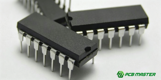
A Dual Inline Package (DIP) is a type of electronic component packaging used to house integrated circuits (ICs). It consists of a rectangular body with two rows of pins on either side that are used to connect the component to a circuit board. Each pin in the DIP corresponds to an electrical connection that allows the IC to interact with other components on the circuit board. The pins are usually arranged in a standardized pattern, making it easier to connect to the board through holes.
DIP is particularly well-known for its through-hole mounting design, where the pins are inserted into holes on a printed circuit board (PCB) and soldered to secure the component. This design contrasts with Surface-Mount Devices (SMD), where components are mounted directly onto the surface of the PCB, without the need for holes.
History and Evolution of DIP
The Dual Inline Package (DIP) was introduced in the 1960s during the early stages of the electronics revolution. It became the standard package for most integrated circuits (ICs) at the time, as it provided a simple and reliable way to mount components on a PCB. DIPs were widely used in consumer electronics, early computers, and communication devices. The design allowed for easy insertion and removal of components, which was especially useful in the early stages of mass production when devices needed to be frequently updated or repaired.
In the early days of electronics, through-hole technology (which includes DIP) was the primary method for connecting components to circuit boards. As technology advanced and components became smaller, manufacturers began developing more compact alternatives like Surface-Mount Devices (SMD). However, DIP remained popular for many years due to its ease of use, durability, and lower cost for low-volume production.
Today, DIP is less common in high-volume, modern electronics, but it still plays a key role in prototyping, educational kits, and legacy systems that require manual assembly. It is a great choice for hobbyists, engineers working with low-volume applications, and for situations where physical handling and ease of soldering are priorities.
How Does a Dual Inline Package (DIP) Work?
A Dual Inline Package (DIP) is an electronic component with a rectangular body and two rows of pins used to connect integrated circuits (ICs) to a circuit board through through-hole mounting.
Electrical Connections and Pin Configuration
A Dual Inline Package (DIP) connects to a circuit board through its pins, which are metal leads that extend from both sides of the package. These pins are inserted into holes drilled into the PCB. When the component is soldered, the pins create electrical connections that allow the circuit to function.
Each pin in a DIP has a specific role, typically corresponding to different signals, power, or ground connections. Some pins provide power (such as VCC or ground), while others may carry data or signal connections to different parts of the circuit. For example, a 14-pin DIP might have several pins dedicated to signal inputs and outputs, with a few for ground and power.
DIPs are often used in low-power circuits, where they serve as the interface between the chip and the rest of the system. The pin configuration is typically standardized, so once the correct layout is known, it's easy to integrate the DIP into a variety of circuits.
Mounting Methods (Through-hole vs. Surface Mounting)
Through-hole mounting is the primary method used for installing DIPs on circuit boards. In this method, the pins on the DIP are inserted into pre-drilled holes on the PCB. After insertion, the pins are soldered to the board, making an electrical connection between the component and the circuit. This process is widely used in low-volume production, prototyping, and DIY electronics because it's easy to handle and can be done manually.
Surface-Mount Technology (SMT) is an alternative method where components are mounted directly onto the surface of the PCB. In contrast to through-hole, Surface-Mount Devices (SMD) do not require holes and are typically smaller, making them better suited for high-density, automated production lines. While SMT offers more compact designs, it can be harder to assemble manually, which is why DIP is still favored for hand-soldering and prototyping.
Comparison: Through-hole vs. Surface Mounting
Feature Through-hole (DIP) Surface-mount (SMD) Assembly Manual soldering possible Requires automated equipment Size Larger components Smaller and compact Application Prototyping, repairs Mass production, high density Durability Strong mechanical bond Weaker mechanical bond Cost Generally cheaper in small volumes More cost-effective for mass production
| Feature | Through-hole (DIP) | Surface-mount (SMD) |
| Assembly | Manual soldering possible | Requires automated equipment |
| Size | Larger components | Smaller and compact |
| Application | Prototyping, repairs | Mass production, high density |
| Durability | Strong mechanical bond | Weaker mechanical bond |
| Cost | Generally cheaper in small volumes | More cost-effective for mass production |
In summary, while through-hole mounting (used by DIPs) is great for ease of assembly, surface-mount offers smaller and more efficient designs for mass production. Both methods have their specific advantages depending on the context of use.
What Are the Key Benefits of Dual Inline Packages (DIP)?
The key benefits of Dual Inline Packages (DIP) include their durability, ease of handling and assembly, and low cost, making them ideal for prototyping, small-scale production, and applications requiring robust connections.
Durability and Mechanical Strength
A Dual Inline Package (DIP) is highly valued in certain robust electronic applications due to its durability and mechanical strength. The through-hole mounting method, where the pins are inserted into holes on a PCB, provides a strong physical connection that can withstand vibrations, mechanical stress, and physical impacts. This makes DIPs ideal for use in industrial equipment, consumer electronics, and outdoor devices that may be exposed to rough conditions.
For example, in older computer hardware or test equipment, DIPs are preferred because they are less prone to damage from handling or environmental factors. The larger, more sturdy structure of DIP components also makes them easier to repair or replace, which is crucial in long-term equipment or field maintenance.
In contrast, Surface-Mount Devices (SMD), though smaller, are less durable in some applications, particularly when it comes to mechanical stress and handling. This durability makes DIP a go-to choice for many applications that require physical resilience.
Easy to Handle and Assemble
DIP components are much easier to handle and assemble compared to modern Surface-Mount Devices (SMD). One key advantage of DIP is its larger size and through-hole mounting, which makes it easier to physically insert, position, and solder onto a Printed Circuit Board (PCB).
For hobbyists, prototyping, or small-scale production, this ease of assembly is invaluable. Unlike SMDs, which often require specialized equipment for automated placement and soldering, DIPs can be manually soldered with simple tools like a soldering iron. This allows for quick fixes and troubleshooting without the need for expensive machinery.
Additionally, because the pins are accessible from both sides, it’s much easier to visually inspect connections and identify problems. This is especially important when troubleshooting circuits or making quick modifications during the development process.
Low Cost and Availability
DIPs are known for their low cost, particularly when used for small-scale production or prototyping. The relatively simple design and manufacturing process make them one of the most affordable options for electronic components. This affordability is one reason why DIPs are still commonly used in educational kits, DIY electronics projects, and small businesses.
Another factor is the wide availability of DIP components in the market. Since DIPs have been around for many years, they are easy to source and often come in a wide range of options, from basic logic ICs to microcontrollers and operational amplifiers. This makes them a go-to option for engineers and hobbyists who need quick access to reliable, low-cost components.
While newer packaging methods like SMD are more cost-effective for high-volume manufacturing, DIPs remain a great choice for projects where the production volume is low, and cost-efficiency is critical.
What Are the Main Applications of Dual Inline Packages (DIP)?
Dual Inline Packages (DIP) are widely used in consumer electronics, industrial machinery, and prototyping projects due to their durability, ease of assembly, and cost-effectiveness, particularly for low-volume and hands-on applications.
Use in Consumer Electronics
DIPs continue to be used in consumer electronics despite the growth of smaller packaging options. Their simplicity, durability, and ease of assembly make them a practical choice for various consumer devices. Radios, televisions, and gaming consoles from earlier generations often relied on DIP components. For example, older models of stereos and TV sets used DIP-based ICs for audio processing, signal routing, and control functions.
While newer models may have shifted to Surface-Mount Devices (SMD) for space-saving reasons, many retro electronics and vintage gaming consoles still feature DIPs. Enthusiasts and repair technicians often prefer these components when restoring or modifying older consumer electronics, as their larger size and through-hole design make them easier to replace and troubleshoot.
In modern consumer electronics, DIPs may still be found in audio equipment, microwave ovens, and other household devices that don’t require the smallest form factor but do benefit from the robustness of DIP connections.
Use in Industrial Electronics
In industrial electronics, DIPs are used in machinery, sensors, and control systems that require high reliability and strong physical connections. DIPs’ mechanical strength makes them ideal for applications where electronic components need to endure heavy vibrations, heat, or physical impacts. For instance, industrial sensors, control systems, and automation equipment often use DIPs for connecting microcontrollers, timing circuits, and signal processing units.
One example is factory automation equipment, where the DIP components' durability helps the systems withstand the harsh conditions of industrial environments. Additionally, machine controllers and robotic systems frequently rely on DIPs to ensure that the components remain intact during installation or maintenance. Their through-hole mounting also allows for easier repairs in the field, which is crucial in industrial settings where downtime is costly.
Use in Prototyping and DIY Projects
For hobbyists and engineers working on prototyping or DIY electronics, DIPs are extremely popular due to their ease of use and availability. In prototype circuit boards and breadboards, DIPs are ideal because they are easy to insert and remove, which allows for quick testing and modifications. Many starter kits for electronics come with DIPs, as they are simple to work with and don't require specialized tools for soldering.
DIPs are commonly used in educational projects, such as learning about microcontrollers or basic circuit design, where hands-on assembly is encouraged. In the maker community, Arduino and Raspberry Pi boards may also include DIPs for specific components, making it easier for DIYers to modify or replace parts as needed.
Additionally, in small-scale production or for limited-run projects, DIPs provide a cost-effective and flexible solution, allowing engineers to prototype and iterate on designs before transitioning to more complex packaging types like SMD.
What Are the Limitations of Dual Inline Packages (DIP)?
The limitations of Dual Inline Packages (DIP) include their larger size, incompatibility with modern high-volume manufacturing processes, and challenges in heat dissipation, making them less suitable for high-density, high-performance applications.
Size and Component Density
A major limitation of Dual Inline Packages (DIP) is their size. DIPs are relatively large compared to modern packaging types, such as Quad Flat Package (QFP) or Ball Grid Array (BGA). This makes them less ideal for high-density circuit designs where space is limited. As the demand for smaller, more compact electronics grows, the size of the package becomes a significant factor.
For example, a 16-pin DIP occupies more PCB space than the same 16-pin configuration in QFP or BGA packages. This limitation means that fewer components can fit in the same area, making DIPs less suitable for high-performance devices like smartphones, laptops, or tablets.
Comparison Table: DIP vs. QFP vs. BGA
Feature Dual Inline Package (DIP) Quad Flat Package (QFP) Ball Grid Array (BGA) Size Larger, occupies more space Smaller, more compact Most compact, saves space Pin Density Lower pin density Higher pin density Highest pin density Application Low-volume, older designs Mid to high-end applications High-end, performance-driven Cost Low cost, good for small runs Moderate cost Higher cost, for mass production Ease of Assembly Easier to manually assemble Requires automated equipment Requires complex machinery
| Feature | Dual Inline Package (DIP) | Quad Flat Package (QFP) | Ball Grid Array (BGA) |
| Size | Larger, occupies more space | Smaller, more compact | Most compact, saves space |
| Pin Density | Lower pin density | Higher pin density | Highest pin density |
| Application | Low-volume, older designs | Mid to high-end applications | High-end, performance-driven |
| Cost | Low cost, good for small runs | Moderate cost | Higher cost, for mass production |
| Ease of Assembly | Easier to manually assemble | Requires automated equipment | Requires complex machinery |
As the table shows, BGA and QFP are more space-efficient, allowing for higher component density, while DIP is more suited to simpler, low-density applications.
Incompatibility with Modern Manufacturing Processes
DIP is less favored in high-volume, automated PCB manufacturing due to its through-hole design, which requires individual insertion of the pins into pre-drilled holes. This process is slower and less efficient compared to Surface-Mount Technology (SMT), which uses SMD components that are placed directly on the surface of the PCB. SMT is more compatible with modern pick-and-place machines, which can quickly and accurately assemble thousands of components in a short time.
DIP components require manual soldering or wave soldering, making them unsuitable for high-speed, high-volume production lines. Surface-mount components, on the other hand, allow for faster, more automated processes that lower labor costs and increase overall production efficiency. This is why DIP is increasingly being replaced by smaller, more automated alternatives, such as QFP or BGA.
Heat Management Issues
Another limitation of DIP is its heat dissipation. Since DIPs are larger and their pins are mounted through holes on the PCB, they tend to trap more heat, which can affect performance, especially in high-power or high-frequency applications. The larger footprint of DIP components means that heat doesn’t dissipate as efficiently as with more compact packaging types, such as BGA or QFP, which are better suited for managing heat in high-performance circuits.
In high-performance electronics like computers, graphics cards, and servers, managing heat is critical. BGA and QFP packages offer better thermal conductivity because they have more surface area and are mounted closer to the PCB, allowing heat to be distributed more effectively. In contrast, DIP components are more prone to heat buildup, which can lead to overheating and reduced reliability over time. This makes DIP less ideal for devices that generate significant heat or require active cooling solutions.
In summary, while DIP has its advantages in terms of durability and ease of assembly, its limitations in size, manufacturing compatibility, and heat management make it less suitable for modern, high-performance electronic applications.
How Do You Choose Between DIP and Other Package Types?
When choosing between DIP and other package types, consider factors like production volume, space constraints, ease of assembly for prototyping, and cost—DIP is best for small runs and DIY projects, while alternatives like QFP or BGA are more suitable for high-density, high-volume applications.
Considerations for Low-volume vs. High-volume Production
When deciding between Dual Inline Package (DIP) and other package types like QFP or BGA, the key factor is the production volume.
For low-volume production or small runs, DIP is often the best choice. Its simple design and easy assembly process make it cost-effective for small quantities. Since DIPs are easier to handle and don’t require specialized machinery, they are perfect for small-scale projects, prototypes, or educational kits.
On the other hand, for high-volume production, QFP or BGA are typically more efficient. These packages are smaller and more compact, allowing for higher component density, which is crucial for modern electronics. Automated assembly processes, such as pick-and-place machines, can easily place and solder SMD components like QFP and BGA, significantly reducing labor costs and increasing production speed. In high-volume settings, DIP becomes less practical due to the need for manual soldering and the large space required on the PCB.
Factors to Consider for DIY and Prototyping
For DIY projects and prototyping, DIPs are often the preferred choice. This is because DIPs are easier to handle and solder, especially for those without access to advanced tools. Many hobbyists and engineers working on prototypes find that DIPs provide a quick and efficient way to test circuit designs without needing complex equipment.
When prototyping, DIP components can be easily inserted into breadboards or PCB prototypes, making them an ideal choice for testing circuits. Unlike SMD components, which often require precision placement tools and specialized soldering techniques, DIPs can be manually inserted and soldered with basic tools. This accessibility makes DIPs a great choice for early-stage designs or learning environments where speed and simplicity are key.
Cost and Space Constraints in Circuit Design
When choosing between DIP and other package types, cost and available space are two of the most important factors to consider.
DIP is cost-effective for low-volume designs because it is simple to manufacture, and manual assembly is feasible. However, when space is limited or a higher pin density is needed, alternative package types like QFP or BGA become more favorable. These packages allow for more components in a smaller area, which is ideal for compact consumer electronics like smartphones or wearables.
In circuits with limited space, DIP’s larger size and wider pin spacing may not be suitable. Choosing QFP or BGA allows designers to fit more components into a smaller PCB footprint. However, these options can be more expensive and require specialized equipment for assembly. Thus, the decision comes down to balancing cost efficiency with the space constraints of your specific design.
Conclusion
While Dual Inline Packages (DIP) offer several benefits such as durability, ease of assembly, and cost-effectiveness for small-scale production and prototyping, they do have limitations when compared to more compact modern packaging options like QFP and BGA. When selecting the right package type, it’s important to consider factors like production volume, space constraints, and specific application needs.
As a seasoned PCB and PCBA supplier, PCBMASTER understands the importance of choosing the right components for your projects. With years of experience in providing high-quality PCBs and assembly services, PCBMASTER is dedicated to helping you find the best solutions for your designs. Whether you're prototyping, assembling for low-volume production, or moving into high-performance applications, we offer tailored support to ensure your success. Reach out to us for top-tier components and expert guidance for your next project.
FAQs
1. Why is DIP still used in certain electronic products despite the rise of SMD?
DIP (Dual Inline Package) continues to be used in certain electronic products for several reasons, despite the widespread adoption of SMD (Surface-Mount Devices).
Ease of repair and replacement is one of the primary reasons DIP remains relevant. In products like vintage electronics, radios, and older computer systems, DIPs allow for easy manual soldering, making repairs and replacements simpler. The larger pins and accessible layout of the DIP package make it much easier for technicians or hobbyists to handle, especially when dealing with faulty or outdated components.
Additionally, niche markets where physical durability and manual assembly are necessary still favor DIP. For example, in low-volume production or custom-built devices (such as educational kits or specific industrial equipment), DIP offers a balance of reliability and ease of use that SMD components do not.
While SMD is more compact and cost-efficient for mass production, DIP offers affordability and simplicity in low-volume and repairable applications. This is why many electronics, particularly older or retro tech, continue to rely on DIP components.
2. Can I use DIP for high-frequency applications?
DIP is generally not suitable for high-frequency applications due to its physical design, which can negatively impact signal integrity and performance.
At high frequencies, components need to minimize parasitic inductance and capacitance, which can interfere with the signal and reduce the overall performance. The larger size and longer leads of DIP components create more parasitic inductance compared to SMD components, which are much smaller and sit closer to the PCB.
For high-frequency circuits—like those used in RF (radio frequency) applications or high-speed communication devices—alternatives like BGA (Ball Grid Array) or QFP (Quad Flat Package) are preferred. These packages offer better thermal performance and lower parasitic effects, making them better suited for high-speed, high-frequency circuits.
3. What is the difference between a DIP and a TQFP (Thin Quad Flat Package)?
The key differences between DIP and TQFP (Thin Quad Flat Package) are related to size, ease of assembly, and applications.
l Size: TQFP is much smaller and thinner than DIP. While DIP has two rows of pins and requires through-hole mounting, TQFP has pins arranged on all four sides and uses surface-mount technology (SMT). This allows TQFP to fit in much smaller spaces, making it ideal for applications with space constraints.
l Ease of Assembly: DIP is easier to hand-solder since it’s larger, and the pins are more accessible for manual insertion into PCB holes. On the other hand, TQFP is more difficult to solder by hand because the leads are finer and require more precision, which is typically handled by automated pick-and-place machines in high-volume manufacturing.
l Applications: DIP is commonly used in low-volume production or prototyping, where manual assembly is common. TQFP, being smaller and more compact, is favored in high-performance electronics like smartphones, laptops, and other devices where space optimization is crucial.
In summary, TQFP offers smaller size and higher pin density but requires automated assembly, while DIP is larger and easier to handle manually but takes up more space.
4. Is it easy to solder a Dual Inline Package by hand?
Yes, DIP is much easier to hand-solder compared to SMD components. There are several reasons for this:
l Larger Pins: The pins of a DIP are thicker and more widely spaced than those of SMD components, making them easier to grab with a soldering iron or soldering tools.
l Through-Hole Design: Because DIP components use through-hole mounting, the pins go through the PCB, allowing for better visibility and easier access during the soldering process. This is much simpler than SMD components, which are placed on the PCB surface and often require more precise soldering techniques.
l Hand-soldering DIP components requires only basic tools, such as a soldering iron, soldering wire, and a soldering pump for rework. SMD components, however, often require hot-air rework stations or soldering paste, making the process more complex for those without specialized equipment.
Overall, for hobbyists or those working on prototypes, DIP is a great choice for manual assembly due to its ease of soldering.
5. What tools do I need to work with DIP in a DIY project?
Working with DIP components for DIY projects requires a few basic tools to ensure proper assembly. Here’s a list of essential tools for soldering and assembling DIP components:
l Soldering Iron: A basic soldering iron (preferably with adjustable temperature) is essential for melting the solder and connecting the pins of the DIP to the PCB.
l Solder: Lead-free solder or rosin-core solder (depending on your preference) is required to make a strong electrical connection.
l Soldering Iron Tip Cleaner: A wet sponge or a tip cleaner will keep your soldering iron tip clean and efficient for precise soldering.
l Tweezers: For positioning the DIP component on the PCB before soldering, a good pair of tweezers will ensure accurate placement.
l PCB (Printed Circuit Board): You'll need a PCB to mount your DIP components. For prototyping, breadboards can also be used.
l Soldering Pump or Desoldering Braid: If you make mistakes, a soldering pump or desoldering braid can help you remove solder and reposition components.
l Multimeter: A multimeter can be used to test the electrical connections and check for continuity after the soldering is complete.
These tools will allow you to solder DIP components easily and accurately for your DIY electronics project.

