


Complete Guide to PCB Materials: Types, Properties, and Sizing
Choosing the right PCB material is crucial to ensuring the reliability and performance of your electronic products. Whether you're designing a consumer gadget, a high-speed communication device, or an energy-efficient lighting solution, the base material of your PCB directly impacts its electrical, mechanical, and thermal characteristics. From the widely-used FR-4 to specialized high-frequency boards, each material serves a specific purpose. But how do you decide which one to use?
This guide dives into the essentials of PCB materials and cutting techniques, offering clear insights into their key properties and applications. We'll break down common material types like FR-4 and metal substrates, explain performance parameters you need to consider, and explore the best practices for optimizing material use during the manufacturing process. If you're ready to make informed choices for your next PCB project, keep reading!
What is PCB Material?
PCB (Printed Circuit Board) material is the foundational component used to build circuit boards for electronic devices. It consists of two main layers: the insulating layer (also called the substrate or dielectric layer) and the conductive layer (often copper). These materials play a critical role in determining the performance, durability, and manufacturing process of a PCB.
Insulating Layer and Conductive Layer
l Insulating Layer: The insulating layer, also known as the substrate, provides electrical isolation between the conductive paths (or traces) on the PCB. This layer is usually made from materials like fiberglass, resin, or plastic. It prevents electrical signals from short-circuiting between different traces.
l Conductive Layer: The conductive layer is typically made of copper foil. It is attached to the insulating layer and is etched to form the electrical pathways that connect different components on the PCB. The copper layer’s quality, thickness, and smoothness affect the performance of the PCB, including its signal integrity and resistance.
For example, in everyday electronics like smartphones or computers, the copper traces connect various chips and components, while the insulating layer ensures no unintended electrical contact occurs between them.
Role of Substrate and Copper Foil Layers
The substrate and copper foil layers together define the structure and electrical properties of a PCB. The substrate provides mechanical strength and supports the copper traces, while the copper foil allows the necessary electrical connections to be made.
For instance, in consumer electronics, such as tablets, the choice of substrate (like FR-4, which is a popular choice) ensures the PCB is durable and can withstand everyday use. Copper foil ensures efficient signal transmission between components. If the copper is too thin, the PCB may struggle with high-frequency applications like wireless communication.
Electrical Performance
PCB materials must have specific electrical properties to perform well in different applications. The key parameters to consider include dielectric constant (Dk) and loss tangent (Df).
l Dielectric Constant (Dk): Dk represents the material's ability to store electrical energy. For example, in high-frequency circuits (like radio transmitters), the lower the Dk value, the less signal loss occurs.
l Loss Tangent (Df): This refers to the signal loss during transmission. Low Df materials are important for high-speed circuits to ensure minimal energy loss and signal degradation.
In applications such as wireless routers or mobile phones, these electrical properties are critical for ensuring fast and reliable signal transmission without interference.
Mechanical Performance
Mechanical performance refers to the material’s ability to endure physical stresses such as pressure, temperature changes, and mechanical stress without failing. The flexibility, strength, and impact resistance of the PCB material play a crucial role in ensuring the PCB can be manufactured and assembled without damage.
For example, in automotive applications where PCBs are exposed to high vibrations and temperature changes, materials with higher mechanical strength, like high-Tg (glass transition temperature) FR-4, are preferred. These materials help maintain the integrity of the PCB in harsh conditions.
Thermal Performance and Heat Dissipation
Heat dissipation is crucial for preventing electronic components from overheating, which could lead to failure. PCB materials with good thermal conductivity help in efficiently dissipating heat away from sensitive components.
l Thermal Conductivity: Materials with high thermal conductivity, such as metal-based PCBs (e.g., aluminum-backed PCBs), are ideal for applications like LED lighting or power electronics, where heat is generated in large amounts.
l Thermal Expansion: A material’s coefficient of thermal expansion (CTE) is the rate at which it expands or contracts with temperature changes. Low CTE is crucial for maintaining the integrity of solder joints and preventing failure over time, especially in circuits that go through multiple thermal cycles.
For instance, in power electronics, choosing a PCB material with high thermal conductivity ensures that the heat generated by power components (like transistors or capacitors) can be efficiently managed, preventing potential damage from overheating.
What Are the Common Types of PCB Materials and Their Applications?
PCB materials come in various types, each designed to meet the specific needs of different electronic devices. Understanding the differences can help you choose the right material for your project. Here, we explore three common types of PCB materials: FR-4, High-Frequency/High-Speed materials, and Metal-Based PCBs.
FR-4 PCB: The Most Common PCB Material
What is FR-4?
FR-4 is the most widely used PCB material due to its balanced performance and cost-effectiveness. It is composed of fiberglass and epoxy resin. The fiberglass provides mechanical strength, while the epoxy resin offers electrical insulation and durability. FR-4 has good electrical properties and is resistant to heat and flame, making it suitable for general-purpose electronic applications.
Key Characteristics:
l Cost-Effective: FR-4 is inexpensive compared to other specialized materials.
l Durable: With a glass transition temperature (Tg) typically around 130–140°C, FR-4 can withstand moderate heat.
l Stable: It offers reliable performance in most everyday electronics.
Applications of FR-4:
l Consumer Electronics: FR-4 is used in devices like smartphones, tablets, and computers.
l Motherboards: Most computer motherboards are made from FR-4 due to its balance of mechanical and electrical properties.
l Industrial Control Boards: FR-4 is also used in industrial machinery for its ability to handle moderate temperatures and mechanical stress.
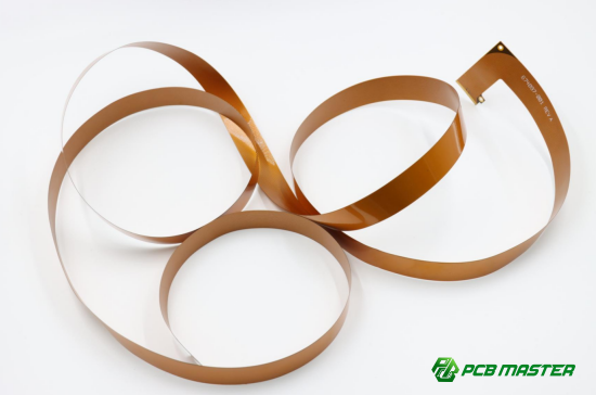
High-Frequency/High-Speed PCBs: Used for Specialized Applications
What Are High-Frequency/High-Speed PCBs?
High-frequency and high-speed PCBs are designed for applications where signal integrity and minimal loss are critical. These materials are made from special compounds such as polytetrafluoroethylene (PTFE), ceramic fillers, and hydrocarbon-based materials. These materials have low dielectric constants (Dk) and low loss tangents (Df), which means they allow signals to travel faster with minimal distortion.
Key Characteristics:
l Low Dk: This property reduces signal delay and ensures fast data transmission.
l Low Df: Low loss means that very little energy is lost as signals travel through the PCB, improving performance.
Applications of High-Frequency/High-Speed PCBs:
l Radar Systems: High-speed PCBs are essential for radar systems, where fast signal processing is critical.
l Satellite Communication: These PCBs are used in satellite communication systems, where high-frequency signals are transmitted over long distances.
l Telecommunication Equipment: Devices like base stations and antennas also rely on these PCBs for clear and fast signal transmission.
Metal-Based PCBs: Excellent Heat Dissipation
What Are Metal-Based PCBs?
Metal-based PCBs (often referred to as MCBs) feature a metal core—usually aluminum or copper—which provides superior heat dissipation. These materials are particularly effective for applications that generate a lot of heat, as the metal quickly transfers heat away from sensitive components, preventing overheating.
Key Characteristics:
l Thermal Conductivity: Metal-based PCBs have high thermal conductivity, which allows them to efficiently manage heat.
l Mechanical Strength: The metal core also adds extra mechanical strength, which is useful in harsh environments.
Applications of Metal-Based PCBs:
l LED Lighting: Metal-based PCBs are commonly used in LED lighting systems where high heat generation is a concern. The metal core helps cool down the components to prevent failure.
l Power Modules: In power electronics, where significant heat is generated, metal-based PCBs are ideal for keeping the system cool and running efficiently.
l Automotive Electronics: These PCBs are used in automotive applications, such as power management systems and lighting, where heat dissipation is crucial for longevity.
Choosing the Right PCB Material
Selecting the right PCB material depends on your application’s specific needs. Each type of PCB material offers distinct advantages based on its intended use. FR-4 is a versatile and cost-effective option for everyday devices. High-frequency PCBs are required for high-speed, high-frequency communication and signal transmission. Metal-based PCBs, on the other hand, are critical for applications with heat-sensitive components, such as LED lighting or power modules.
Understanding these different materials can help you make an informed decision based on performance, cost, and reliability requirements. Here's a simple comparison of these materials to help clarify their key differences and applications:
| Material Type | Key Features | Best Suited For | Example Applications |
| FR-4 | Cost-effective, durable, versatile | General-purpose electronics with moderate performance needs | Computer motherboards, consumer electronics |
| High-Frequency PCBs | Low Dk and Df, fast signal transmission | High-speed, high-frequency signal processing | Radar systems, satellite communication |
| Metal-Based PCBs | High thermal conductivity, heat dissipation | Heat-sensitive applications | LED lighting, power modules, automotive systems |
By examining these key features and use cases, it becomes easier to match the right material to your specific application needs. For instance:
l FR-4 is an ideal choice for designing computer motherboards due to its cost-effectiveness and durability.
l For high-performance systems such as radar systems or satellite communication devices, high-frequency PCBs with PTFE materials are necessary to ensure fast signal transmission with minimal loss.
l In applications like LED lighting, where heat is a concern, metal-based PCBs are perfect for efficient heat dissipation to keep components cool and functional.
By understanding the differences in materials and their specific applications, you can select the best PCB material to ensure your electronic products perform optimally while remaining durable and cost-effective.
What Are the Key Performance Parameters of PCB Materials?
PCB materials need to meet several important performance parameters to ensure they function properly in different environments. These parameters include Tg (Glass Transition Temperature), Td (Thermal Decomposition Temperature), Dk (Dielectric Constant), Df (Loss Tangent), CTE (Coefficient of Thermal Expansion), and CAF (Ion Migration Resistance). Let's break down each one.
Tg (Glass Transition Temperature) and Heat Resistance
What is Tg?
Tg, or Glass Transition Temperature, refers to the temperature at which a PCB material begins to soften and lose its rigid, solid state. Materials with a higher Tg can withstand higher temperatures without warping or losing their electrical properties. The Tg value directly impacts a PCB’s heat resistance, which is critical in high-temperature environments.
Difference Between Standard and High-Tg Boards:
l Standard Tg materials (e.g., FR-4) typically have a Tg between 130°C and 140°C, making them suitable for most consumer electronics and standard industrial applications.
l High-Tg materials have a Tg of 150°C or higher, offering enhanced heat resistance and stability. These materials are ideal for environments where the PCB is exposed to higher temperatures, such as in automotive, aerospace, or high-performance computing applications.
For instance, a high-Tg PCB is often used in automotive electronics to withstand the heat generated by engine components, ensuring long-term reliability.
Td (Thermal Decomposition Temperature) and Material Stability
What is Td?
Td, or Thermal Decomposition Temperature, is the temperature at which a PCB material begins to chemically break down. Materials with a higher Td offer better thermal stability and can endure extreme heat without degrading or losing functionality.
Advantages of High Td Materials:
l Higher Td materials can withstand prolonged exposure to heat without breaking down.
l They are essential in environments where the PCB will encounter high temperatures or fluctuating heat levels.
For example, in power electronics or LED lighting, components often generate heat. Using a material with a high Td ensures that the PCB will not fail or degrade under these thermal stresses.
Dk (Dielectric Constant) and Signal Transmission Speed
What is Dk?
Dielectric Constant (Dk) is a measure of a material's ability to store electrical energy in an electric field. A low Dk value means that the PCB material has a lower signal delay, allowing faster signal transmission.
Dk’s Importance for High-Frequency Circuits:
l For high-frequency applications like radar systems or wireless communication, a low Dk value is essential. It reduces signal delay, allowing signals to propagate faster and with less distortion.
l High-frequency PCBs use materials like PTFE (polytetrafluoroethylene) which have a low Dk, enabling high-speed data transmission.
For example, satellite communication systems rely on low Dk materials to transmit high-frequency signals quickly and efficiently over long distances.
Df (Loss Tangent) and Signal Loss
What is Df?
Loss Tangent (Df) is a measure of the energy lost as a signal travels through a PCB material. A low Df value means that less energy is lost during signal transmission, which is critical for high-speed applications.
Df’s Role in High-Frequency Applications:
l Low Df materials are essential in circuits where signal integrity is critical, such as 5G communications, high-speed data centers, and high-frequency radar systems.
l Materials like ceramic-filled PTFE have low Df and are commonly used in these high-frequency applications to ensure efficient and reliable performance.
For example, 5G mobile networks rely on low Df materials to minimize signal loss, ensuring high-speed data transmission and reducing latency.
CTE (Coefficient of Thermal Expansion) and Material Reliability
What is CTE?
Coefficient of Thermal Expansion (CTE) refers to how much a material expands or contracts when its temperature changes. PCB materials with low CTE are more stable and are less likely to warp or crack due to thermal cycling (the process of repeatedly heating and cooling).
Importance of Z-Axis CTE:
l Z-axis CTE (expansion along the thickness of the PCB) is the most critical factor, as it affects the reliability of solder joints and electrical connections. If the material expands too much in the Z-axis, it can cause cracks in the solder joints, leading to PCB failure.
l Low Z-axis CTE ensures that the PCB can withstand multiple reflow soldering cycles without mechanical failure.
For instance, in automotive electronics, where PCBs undergo frequent temperature changes, low CTE is crucial for ensuring the board remains intact during operation and through thermal cycling.
CAF (Ion Migration Resistance) and Stability in Humid Environments
What is CAF?
CAF (Conductive Anodic Filament) is the phenomenon where ions migrate through the PCB material, causing electrical shorts under high temperature and humidity. Materials with high CAF resistance prevent these shorts, ensuring that the PCB remains functional even in harsh environments.
CAF Resistance and High-Temperature, High-Humidity Environments:
l CAF resistance is especially important in high-humidity and high-temperature environments, where ion migration is more likely to occur.
l High-CAF resistant materials are commonly used in aerospace and military applications, where environmental conditions are extreme.
For example, military-grade PCBs used in radar systems are often designed with high CAF resistance to ensure that they remain operational in humid, high-heat conditions.
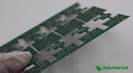
What Does PCB Cutting Mean?
PCB cutting refers to the process of cutting large sheets of PCB material into smaller panels or pieces suitable for the manufacturing process. This is done to maximize material usage and ensure that the final PCB products meet specific design requirements. Understanding the various stages and factors involved in this process is critical for optimizing production efficiency and minimizing waste.
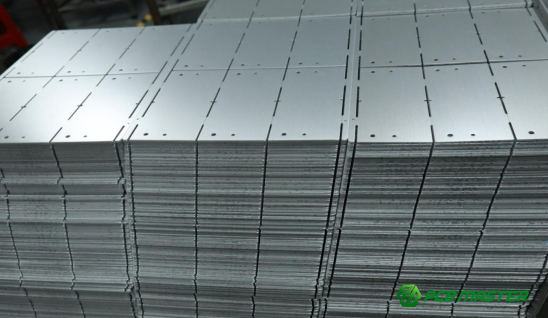
Standard Large Material Sizes and Their Role
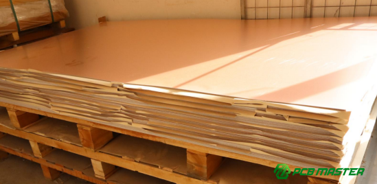
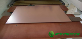
What are standard large material sizes?
Standard large material sizes are the initial dimensions of the PCB material sheets provided by suppliers. These sheets serve as the basic units from which the smaller, usable PCB panels are cut. By using standardized sizes, manufacturers can ensure consistency in production and streamline the procurement process.
Common Standard Sizes:
l 36" × 48"
l 40" × 48"
l 42" × 48"
These sizes are typically used for rigid FR-4 materials, which are the most common PCB materials. The choice of large material size impacts the overall layout and efficiency of PCB cutting. For example, a 40" × 48" sheet is often chosen for mass production as it offers an optimal balance between material availability and processing ease.
Using standard sizes allows manufacturers to manage their inventory efficiently and predict material costs more accurately.
How to Determine the Panel Size for Production
What is production panel sizing?
Production panel sizing refers to the process of cutting down the large material sheets into smaller, more manageable panels. This size is critical because it must fit the capabilities of the PCB production line while maximizing material usage.
Maximizing Material Utilization:
To maximize the use of each large material sheet, engineers use specialized software to arrange the panels within the material sheet. The goal is to optimize the layout so that as much material as possible is used without excess waste. This is called nesting.
For example, if you're producing a batch of smartphone PCBs, the software will calculate how to arrange as many pieces as possible from each large sheet, considering component size and spacing requirements.
Factors Affecting Production Panel Size
What factors influence the choice of panel size?
Several factors can influence the size of the production panels, including:
l Equipment Capability: Each PCB production machine, like exposure machines and etching lines, has specific limitations regarding the maximum and minimum sizes it can handle. These limitations dictate the panel size choices.
l Production Efficiency: The panel size must also be optimized for production flow. If panels are too large or too small, it could cause inefficiencies in handling, transport, or machine setup time.
l Design Specifications: The final design of the PCB will dictate the space and layout needed, which affects the panel size.
How Equipment Capabilities Influence Panel Size Selection
How does equipment capability affect panel size?
Each piece of equipment used in PCB production (such as exposure machines, drilling machines, and soldering lines) has its own size limitations. This means that the size of the production panel must fall within the specifications of the equipment.
For example, if a laser etching machine can only process panels up to 20" × 24", then the production panels cannot exceed that size, regardless of the initial material sheet size. Thus, it's essential to align the panel dimensions with the capabilities of the entire production line to avoid disruptions and ensure smooth processing.
How Production Efficiency Relates to Panel Size
How does panel size impact production efficiency?
The size of the panels affects how easily they can be handled during the manufacturing process. Larger panels are typically harder to handle, transport, and work with, which can slow down the production speed and reduce overall efficiency. Smaller panels, on the other hand, are easier to manipulate but may lead to higher material waste if not optimally arranged.
Balancing Panel Size and Efficiency:
l Moderate-sized panels are often chosen because they balance ease of handling with minimal waste.
l In high-volume production, optimizing panel size helps improve production rates and reduce material costs.
For instance, in the production of consumer electronics like laptops or tablets, manufacturers often choose moderate-sized panels to ensure a quick turnaround while maintaining a high material yield.
How to Ensure Maximum Material Utilization
What steps can be taken to maximize material utilization?
To ensure that every large sheet of PCB material is used efficiently, manufacturers use specialized software tools to plan and layout the cutting process. These tools allow engineers to:
1. Optimize panel arrangement by fitting as many panels as possible into the available space on the large material sheet.
2. Account for panel shape: The layout should avoid leaving empty gaps or small leftover pieces.
3. Adjust for equipment constraints: Ensure that the panel size chosen fits within the machinery’s capabilities.
For example, in high-volume PCB manufacturing, optimizing panel cutting helps reduce material waste and production costs, which is crucial for maintaining competitive pricing and sustainability.
How to Choose the Right PCB Material and Cutting Size?
Choosing the appropriate PCB material and cutting size is crucial for ensuring that your product performs well, is cost-efficient, and meets manufacturing standards. The material choice directly influences the electrical, mechanical, and thermal properties of the PCB, while the cutting size affects production efficiency and material utilization. Here's how to make these decisions effectively.
Choosing the Material Based on Product Requirements
How do product requirements affect material selection?
The selection of PCB material depends largely on the specific functional requirements of the product. For example:
l Electrical Requirements: If your product needs to handle high-speed signals or high-frequency communications, materials like PTFE (polytetrafluoroethylene) or ceramic-filled PTFE are ideal. These materials offer low dielectric constant (Dk) and low loss tangent (Df), minimizing signal loss and improving performance in telecommunications, radar systems, or 5G devices.
l Thermal Requirements: If your product generates a lot of heat, such as in LED lighting or power electronics, choosing a metal-based PCB (like aluminum-backed PCB) is essential. These materials have excellent thermal conductivity, ensuring efficient heat dissipation and preventing overheating.
l Mechanical Strength: For applications exposed to physical stress or extreme environments, high-Tg (high glass transition temperature) materials offer better mechanical strength and can withstand higher temperatures. These are common in automotive electronics or aerospace applications, where reliability is critical under harsh conditions.
By matching the material's properties to the product's specific demands, you ensure the PCB will meet the required performance standards while maintaining durability.
How to Choose Cutting Sizes Based on Production Requirements
How to balance material utilization and production efficiency?
Choosing the right cutting size for PCB panels is essential for maximizing material use and ensuring efficient production. Here’s how to make the best choice:
l Material Utilization: To reduce waste, cutting size should be chosen in a way that fits as many PCB panels as possible into the large material sheets (e.g., 36" × 48" or 40" × 48"). Specialized nesting software can be used to optimize this layout, ensuring that the panels are arranged efficiently, and minimum material is wasted.
l Production Efficiency: The panel size should also be manageable for the production line. For example, if the panels are too large, they may be harder to handle and transport, slowing down production. If the panels are too small, you might produce excess scrap or need more setup time for the machinery.
l Equipment Compatibility: Each piece of PCB manufacturing equipment (e.g., etching machines, drilling machines) has size limitations. The cutting size must fit the specifications of all machines used in production to ensure smooth processing. Choosing a panel size that fits within these limits helps streamline the entire manufacturing process.
For instance, in the production of consumer electronics, manufacturers might choose medium-sized panels that offer a balance between material usage and production speed, while still ensuring the panels are compatible with all equipment.
By selecting the correct cutting size, manufacturers can reduce material waste and improve production speed, leading to cost savings and optimized performance. Balancing these factors ensures the final PCB meets both the functional needs of the product and the production goals of the manufacturer.
Conclusion
Selecting the right PCB material and cutting size is a vital step in ensuring the performance, durability, and efficiency of your product. By aligning material properties with your product's specific needs and optimizing panel sizes for production, you can significantly enhance both product quality and manufacturing efficiency. Whether you are working with consumer electronics, automotive applications, or high-frequency devices, understanding these key factors will help streamline your design and production process.
If you're looking for a trusted partner to guide you through the complexities of PCB material selection and cutting, PCBMASTER is here to help. With years of expertise in PCB and PCBA manufacturing, PCBMASTER offers top-quality solutions tailored to meet your specific requirements. Let us help you bring your electronic products to life with precision and efficiency.
FAQs
1. How to Determine Which PCB Material is Suitable for My Project?
To choose the right PCB material for your project, you need to consider several key factors:
l Electrical Performance: If your project requires high-frequency or high-speed signals, materials like PTFE or ceramic-filled composites are ideal due to their low dielectric constant (Dk) and low loss tangent (Df).
l Thermal Requirements: For heat-sensitive applications (like LED lighting or power modules), a metal-based PCB with materials such as aluminum or copper is preferred for their excellent thermal conductivity.
l Mechanical Strength: If your project will be exposed to mechanical stress or harsh environments, choose materials with higher glass transition temperature (Tg), such as high-Tg FR-4, to ensure durability.
l FR-4 is a cost-effective and versatile material suitable for most consumer electronics and general applications.
By matching your project's electrical, thermal, and mechanical needs with the right material properties, you can make a well-informed choice.
2. Does the Tg Value Have a Significant Impact on PCB Performance?
Yes, the Tg value (Glass Transition Temperature) plays a crucial role in determining a PCB’s thermal performance. The higher the Tg, the better the PCB can withstand high temperatures without softening or deforming. For most standard applications, FR-4 with a Tg of around 130–140°C works well. However, for applications exposed to higher temperatures, like automotive electronics or aerospace systems, a high-Tg material (with a Tg of 150°C or higher) is required to ensure thermal stability and prevent failure under extreme heat conditions.
3. What Are the Advantages of Metal-Based PCBs Over FR-4?
Metal-based PCBs, such as aluminum-based or copper-based PCBs, offer several advantages over FR-4:
l Better Heat Dissipation: Metal-based PCBs have superior thermal conductivity, making them ideal for heat-sensitive components like LEDs and power modules.
l Enhanced Durability: They are more robust in high-power applications, where heat management is critical for long-term performance and reliability.
l Fewer Thermal Stresses: The metal base helps absorb heat, reducing the risk of thermal expansion and ensuring stable performance over time.
In contrast, FR-4 is more affordable and suitable for applications where thermal management is not as critical.
4. What Are the Most Important Factors When Choosing the Right Cutting Size?
When selecting the appropriate cutting size for your PCB panels, several factors must be considered:
l Material Utilization: The cutting size should maximize the use of each large material sheet (e.g., 36" × 48" or 40" × 48") by minimizing waste and ensuring as many panels as possible are cut from the sheet.
l Production Efficiency: The panel size should be compatible with the manufacturing equipment to ensure efficient handling and processing. Very large panels may be difficult to manage, while very small ones may lead to excess scrap or longer setup times.
l Machine Capacity: Ensure that the panel size fits within the equipment's size limits (e.g., exposure machines, drilling machines) to avoid production delays or quality issues.
Balancing these factors helps improve material yield and ensures that production runs smoothly.
5. Why Should You Care About CTE and CAF Performance?
Both CTE (Coefficient of Thermal Expansion) and CAF (Conductive Anodic Filament) are critical for PCB reliability:
l CTE: The Z-axis CTE (thermal expansion along the PCB thickness) must be low to prevent stress on solder joints during thermal cycling (e.g., multiple reflow soldering processes). High CTE can lead to cracking or failure in the connections, reducing the PCB's lifespan.
l CAF: CAF resistance is vital for ensuring that high-temperature and high-humidity environments do not cause ion migration, leading to short circuits or electrical failure. This is especially crucial for aerospace or military applications, where reliability in extreme conditions is paramount.
Focusing on low CTE and high CAF resistance ensures that your PCB remains stable and operational under challenging conditions.

