


DIY Printed Circuit Board for Beginners: A Step-by-Step Guide
Creating your own printed circuit board may sound like a complex task reserved for professional engineers, but the reality is far more approachable. With a few basic tools, a bit of patience, and a willingness to experiment, even beginners can turn a simple electronic idea into a functional PCB. From powering small LED projects to building custom electronics for hobbies, the ability to design and assemble your own boards opens up a world of creative possibilities. This guide walks you through the essential steps, providing practical tips and insights to help you get started confidently.
Introduction to DIY Printed Circuit Boards (PCBs)
What is a Printed Circuit Board?
A printed circuit board (PCB) is a flat board used to connect and support electronic components. It provides both a physical platform and an electrical pathway for components like resistors, capacitors, and microchips. In simple terms, a PCB acts as the backbone of electronic circuits, allowing electricity to flow between components in a controlled and organized way. Understanding basic PCB concepts for beginners is essential for anyone starting with electronics because it lays the foundation for designing and assembling functional circuits.
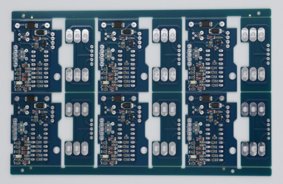
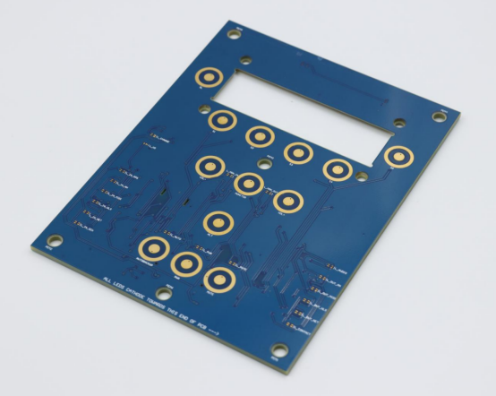
PCBs come in several types based on complexity. A single-layer PCB has copper traces on one side and is ideal for simple circuits like LED blinkers or small sensor projects. Double-layer PCBs have traces on both sides, which allows more complex circuit layouts without increasing board size. Multi-layer PCBs contain three or more conductive layers separated by insulating material, enabling dense circuits such as those used in computers or smartphones. Comparing these types helps beginners choose the right board for their projects: start simple and gradually explore more layers as your skills grow.
Why DIY PCBs are Useful
Creating your own PCB can be more cost-effective than buying pre-manufactured boards, especially for small projects. Off-the-shelf PCBs may include extra features you don’t need, while DIY PCBs allow you to design only what’s necessary, saving both money and materials.
DIY PCB projects also provide hands-on learning. By designing, etching, and assembling a board yourself, you gain practical knowledge of how circuits work, how components interact, and how to troubleshoot common problems. This experience is invaluable for beginners aiming to understand electronics beyond theoretical knowledge.
Another key advantage is rapid prototyping. If you have an idea for a hobby project or a small invention, DIY PCBs let you test and iterate designs quickly. For example, you could create a simple LED blinking circuit on a DIY PCB. By assembling the components and connecting them with traces you designed, you can see the circuit in action, make adjustments, and improve your design before scaling it up. This iterative process encourages experimentation and creativity.
Essential Tools and Materials for DIY PCB Projects
Required Tools for Beginners
A successful DIY PCB project begins with the right tools. PCB design software like KiCad, EasyEDA, or Fritzing allows beginners to create circuit schematics and layout boards digitally. These programs help you visualize connections, arrange components, and export designs for printing or etching. Choosing beginner-friendly software with tutorials can accelerate learning.
Etching equipment is necessary to transfer your design onto the copper board. This includes an etching solution, a container to hold the board, and protective gear such as gloves and goggles. Ferric chloride is a common etchant for hobbyists because it is relatively safe and effective for single- or double-layer PCBs.
Drilling and assembly tools complete the kit. A small handheld drill or drill press is needed for component holes. A soldering iron, along with tweezers, helps in placing and soldering components accurately. Having these tools organized ensures a smoother workflow and reduces mistakes during assembly.
Materials Needed
The base material for any DIY PCB is a copper-clad board, which provides the conductive surface for traces. Additional materials include photoresist sheets or toner paper, depending on your transfer method. These materials help transfer your printed design onto the board for etching.
Electronic components are essential for building functional circuits. Common items for beginners include resistors, LEDs, capacitors, ICs, wires, and solder. Choosing the right components ensures compatibility with your design and prevents unnecessary errors.
A quick comparison of PCB materials can help beginners decide:
Material | Cost | Ease of Use | Durability | Best For |
|---|---|---|---|---|
Single-layer board | Low | Very easy | Moderate | Simple circuits, LEDs |
Double-layer board | Medium | Moderate | Good | More complex circuits |
Multi-layer board | High | Advanced | High | Dense, professional-level boards |
This table highlights the trade-offs between cost, usability, and complexity, guiding beginners in choosing the right material for their projects.
Safety Precautions
Working with chemicals and hot tools requires caution. Always handle etching chemicals safely, avoiding direct skin contact. Store them in labeled, sealed containers away from children or pets.
Ensure proper ventilation in your workspace to avoid inhaling fumes from etching solutions or soldering. A small fan or fume extractor can significantly reduce exposure.
Protective gear is critical for safety. Essential items include chemical-resistant gloves, safety goggles, and a mask for dust or fumes. Additionally, wearing old clothing or an apron protects against spills or burns. Adopting these safety habits early ensures a safe and enjoyable DIY PCB experience.
Step 1 – Designing Your PCB Layout
Choosing a Simple Circuit to Start
When starting with DIY PCBs, it is best to select a simple circuit. Beginner-friendly options include an LED blinking circuit, a small audio amplifier, or an Arduino shield for basic sensors. These projects are straightforward, allow easy testing, and help you understand fundamental PCB design principles. Focusing on easy PCB designs for beginners ensures that you can complete the project without getting overwhelmed by complex layouts or multiple layers.
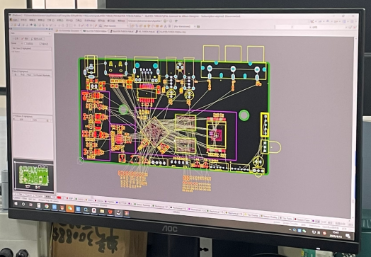
Using PCB Design Software
PCB design software helps you create and visualize your circuit digitally before working on a physical board. Start by creating a schematic, which is a diagram showing all electrical connections between components. Most beginner software like KiCad, EasyEDA, or Fritzing provides simple drag-and-drop tools for placing components and connecting them with wires.
Once the schematic is complete, convert it into a PCB layout. This step translates your design into a physical board with traces and pads where components will be soldered. Use the software’s auto-routing feature for simple designs, or manually adjust traces to optimize the layout. Efficient component arrangement is crucial: group related components together, keep traces short, and avoid crossing paths unnecessarily. This reduces errors and simplifies the etching process.
Design Best Practices
Good PCB design follows basic rules to ensure functionality and durability. Maintain proper trace width and spacing according to the current the circuit will carry. Thicker traces are required for higher currents, while adequate spacing prevents short circuits.
Component placement also affects performance. Place frequently connected components close together and position connectors for easy access. Beginners should avoid common mistakes such as overlapping traces, placing components too close to edges, or leaving insufficient space for soldering.
A practical tip is to review your design before printing or etching. Many software tools include a design rule check (DRC) that highlights spacing or trace issues. Following these best practices ensures that your PCB works correctly the first time, minimizing rework.
Step 2 – Transferring the Design to the PCB
Printing the PCB Layout
The first step in transferring your design is to print the PCB layout. You can use a laser printer to print the design directly onto special transfer paper or use transparency sheets for UV exposure methods. It is crucial to mirror the image before printing so that the traces appear correctly on the copper board after transfer. A mirrored layout ensures that pads and tracks align properly with component leads during assembly.
Transfer Methods
There are two common methods to transfer your PCB design onto the copper board.
1. Toner transfer method: This involves printing the design with a laser printer onto glossy paper or specialized toner transfer paper. The printed design is then pressed onto the cleaned copper board using heat from an iron or laminator. The toner acts as a resist during the etching process. This method is quick, inexpensive, and suitable for single- or double-layer boards.
2. UV photoresist method: In this method, the PCB is coated with a UV-sensitive photoresist layer. The printed transparency with the circuit layout is placed on the board, and the assembly is exposed to UV light. The exposed areas harden, leaving the unexposed areas for etching. This method provides higher precision and is ideal for more detailed or fine-pitch circuits.
Pros and cons comparison:
Method | Precision | Cost | Complexity | Best For |
|---|---|---|---|---|
Toner transfer | Moderate | Low | Easy | Beginner boards, simple circuits |
UV photoresist | High | Medium | Moderate | Detailed layouts, multi-layer |
Preparing the Board
Before transferring the design, the copper surface must be clean. Use fine sandpaper, steel wool, or a scouring pad to remove oxidation and grease. A clean surface ensures that the toner or photoresist adheres properly, preventing incomplete traces.
Once the board is clean, align the printed design carefully before transferring. For the toner method, ensure the paper is positioned correctly and pressed evenly with heat. For the UV method, ensure full contact between the transparency and photoresist layer to avoid blurred or incomplete traces. Proper preparation at this stage reduces errors during etching and increases the likelihood of a successful DIY PCB.
Step 3 – Etching and Cleaning the PCB
Etching Process Explained
Etching removes unwanted copper from the board, leaving only the traces defined by your design. Ferric chloride is the most commonly used etchant for DIY PCBs because it is effective and easy to handle. Alternative etchants like ammonium persulfate or cupric chloride can also be used depending on availability and safety preferences.
The etching process involves immersing the prepared PCB in the etchant solution. Gently agitate the container to ensure the solution reaches all areas and prevents uneven etching. Monitor the progress closely; most simple PCBs take 10–30 minutes depending on the board thickness and etchant concentration. Using proper immersion and agitation techniques ensures clear, accurate traces and reduces the risk of over-etching or incomplete etching.
Post-Etching Cleaning
After etching, the remaining toner or photoresist must be removed to reveal the clean copper traces. For the toner transfer method, use acetone or nail polish remover to wipe off the toner. For UV photoresist, a soft brush with water or developer solution removes the hardened resist.
Once cleaned, inspect all traces carefully. Look for breaks, incomplete etching, or short circuits between traces. A magnifying glass or microscope can help identify small defects that may affect circuit functionality. Early detection of errors allows you to fix problems before soldering components, saving time and frustration.
Tips for a Successful Etch
To achieve a reliable DIY PCB, avoid over-etching, which can thin traces or remove copper from pads, making soldering difficult. Check the board frequently and remove it from the etchant as soon as the unwanted copper is gone.
Troubleshooting common problems includes addressing under-etched areas by gently returning the board to the solution, or correcting shorted traces by scraping away excess copper carefully.
A practical example is comparing a good vs. bad etched PCB: a well-etched board has smooth, complete traces with clear separation, while a poorly etched board may have broken connections or copper bridges. Understanding these differences helps beginners learn to control the etching process effectively.
Step 4 – Drilling and Component Assembly
Drilling Holes for Components
After etching, the PCB needs holes for component leads. Select a drill size that matches each component’s pin diameter. For example, standard resistors or LEDs typically require a 0.8–1.0 mm drill bit. Using the correct size ensures components fit snugly without damaging the board.
For drilling, a drill press provides precision and stability, ideal for multiple or closely spaced holes. A handheld drill is suitable for beginners and small projects but requires careful handling to avoid misaligned or oversized holes. Proper drilling prevents stress on solder joints and ensures the PCB is easy to assemble.
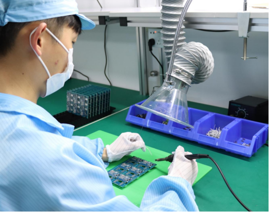
Soldering Components
Soldering connects the electronic components to the PCB and establishes electrical paths. Start by placing components in their correct positions according to the layout. Heat the soldering iron, touch the tip to both the pad and the component lead, and apply solder until it flows evenly. Remove the iron and let the joint cool naturally.
Common mistakes include cold joints, which appear dull or cracked and can interrupt conductivity. These can be fixed by reheating the joint and adding a small amount of solder. Other tips include trimming excess leads and keeping the soldering tip clean.
For example, when assembling a simple LED circuit, place the resistor and LED in their designated spots, solder carefully, and ensure all connections are secure. Following proper soldering steps ensures a reliable and functional PCB.
Testing the PCB
After assembly, continuity testing with a multimeter verifies that all electrical paths are correctly connected. Touch the probes to opposite ends of a trace or component to check for continuity; the meter should beep if the connection is complete.
Next, power the circuit for an initial test. Apply the correct voltage carefully and observe the circuit’s behavior, such as LEDs lighting up or the amplifier producing sound. Testing early allows you to detect errors before completing more complex assemblies, saving time and materials.
Step 5 – Advanced Tips for Better DIY PCBs
Improving Design Precision
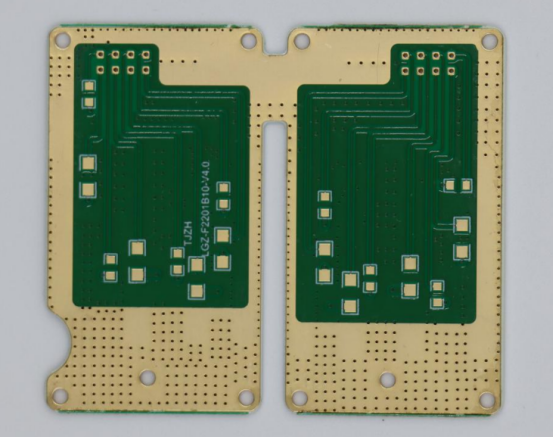
For more advanced DIY projects, double-sided PCBs allow components and traces on both sides of the board. Proper alignment techniques, such as using registration holes or alignment pins, ensure that top and bottom layers match perfectly. This prevents misaligned traces and facilitates more complex designs.
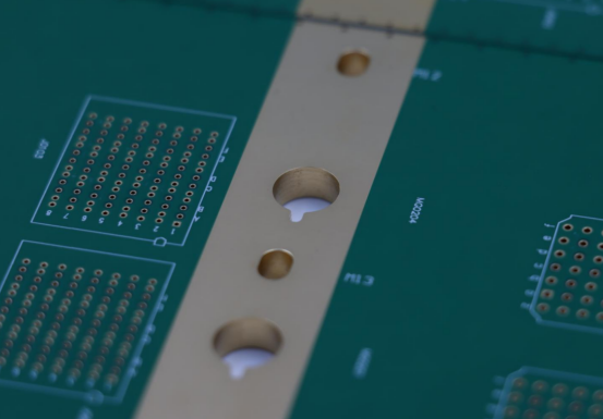
Vias are small plated holes that connect traces between layers. Using vias enables multi-layer routing on double-sided boards, allowing for compact and sophisticated circuits. Beginners can start with a few strategically placed vias to simplify layouts without overwhelming complexity.
PCB Finishing Techniques
Applying a solder mask or protective varnish protects copper traces from oxidation and prevents accidental short circuits. Solder masks also make soldering easier by keeping unwanted areas clear.
Labeling components clearly with text or symbols improves assembly accuracy and troubleshooting. For example, marking resistor values and IC orientations prevents mistakes during soldering and testing. Simple labeling enhances both usability and readability for future modifications.
Troubleshooting and Iteration
Even carefully designed PCBs may encounter issues. Identifying shorts or open circuits is the first step in troubleshooting. Use a multimeter to check connectivity between traces and verify each component’s function.
Iterative design improvements are crucial for learning and refining your skills. After testing, note which areas need adjustment—such as trace width, spacing, or component placement—and update the design before making the next board. Over time, this process helps beginners create more reliable and professional-looking DIY PCBs.
Conclusion
Creating your own DIY printed circuit board opens the door to hands-on learning, creative experimentation, and the satisfaction of turning ideas into functional electronics. From designing simple LED circuits to mastering more advanced multi-layer boards, each step builds essential skills for any electronics enthusiast or hobbyist. For those seeking professional guidance, PCBMASTER is a trusted PCB and PCBA supplier with years of experience. They provide expert advice, technical support, and high-quality manufacturing services, helping you tackle any PCB or PCBA challenge with confidence.
FAQs
Can I make a DIY PCB without a printer?
Yes, it is possible to make a DIY PCB without a printer using hand-drawn methods. You can draw the circuit layout directly onto a copper-clad board using a permanent marker or specialized resist pen. While this method works for very simple circuits, it is less precise than printer-based methods and may require careful cleaning and testing to ensure reliable traces.
How long does it take to create a beginner-level PCB?
For a simple beginner-level PCB, the process typically takes 2–4 hours from design to assembly, depending on complexity. Designing the schematic may take 30–60 minutes, printing and transferring the layout another 30 minutes, etching and cleaning around 30–60 minutes, and soldering components 30–60 minutes. Allow extra time for testing and troubleshooting.
Is etching dangerous, and what precautions should I take?
Etching involves chemicals like ferric chloride, which can be hazardous if mishandled. Always wear gloves, goggles, and protective clothing, work in a well-ventilated area, and store chemicals safely. Avoid direct skin contact, inhalation, or spills, and dispose of used solutions according to local safety regulations.
What is the easiest PCB design software for beginners?
For beginners, EasyEDA and Fritzing are the most user-friendly PCB design software. They provide simple drag-and-drop interfaces, tutorials, and the ability to create schematics and convert them to PCB layouts quickly. KiCad is also free and powerful, though it has a steeper learning curve. Beginners can start with EasyEDA or Fritzing and transition to KiCad as their skills improve.
Can I reuse a DIY PCB if a mistake is made?
Yes, a DIY PCB can sometimes be reused if mistakes occur. Minor errors like solder bridges can be corrected by carefully removing excess solder or scraping away unwanted copper. For larger errors, you can remove components, clean the board, and etch again, effectively giving the board a second life. However, repeated corrections may weaken the board, so careful design and testing are recommended.


