


Quick Turn HDI vs. Traditional PCBs: Key Cost Differences
As the demand for more compact, high-performance electronic devices continues to rise, the pressure on manufacturers to deliver faster, cheaper, and more reliable solutions has never been higher. The evolution of printed circuit boards (PCBs) has been at the heart of this transformation, with Quick Turn HDI PCBs emerging as a powerful alternative to traditional designs. But what does this shift really mean for the industry? While HDI offers impressive capabilities in speed, density, and miniaturization, it’s not always the obvious choice for every project. This article takes a closer look at how Quick Turn HDI and traditional PCBs stack up against each other, shedding light on which technology is the best fit depending on your needs.
Understanding PCB Technology and Its Impact on Electronics Manufacturing
What Are PCBs and Why Are They Essential for Electronics?
Definition and Purpose of Printed Circuit Boards (PCBs)
A Printed Circuit Board (PCB) is a flat, rigid board used in electronic devices to connect electrical components. It consists of layers of conductive material (usually copper) that form electrical pathways, allowing different parts of an electronic circuit to communicate with one another. PCBs provide structural support for the components, while also serving as a platform for routing signals and power. They are essential for all types of electronic products, from smartphones and computers to medical devices and automobiles.
PCBs are typically made from materials like fiberglass, plastic, or resin, with copper traces etched onto their surface. The traces are conductive paths that connect components, enabling signals to flow through the circuit. The board also includes holes (vias) for mounting components and connecting different layers of the PCB. In modern electronics, the design of the PCB significantly impacts the functionality and reliability of the product.
The Role of PCBs in Modern Electronics
In modern electronics, PCBs are more than just a means of connecting components—they enable the performance, reliability, and miniaturization of electronic devices. Without a PCB, an electronic device would be a tangled mess of wires and components, making it nearly impossible to manufacture, assemble, and repair. As devices become smaller and more complex, PCBs have evolved to handle increasingly dense circuit layouts, providing support for high-performance components in compact form factors.
For example, smartphones, which contain multiple processors, sensors, and wireless communication components, rely on advanced PCB designs to function properly. In medical electronics, such as pacemakers, PCBs must not only be compact but also meet stringent reliability and safety standards. This is where the transition from traditional PCB designs to High-Density Interconnect (HDI) technology becomes significant.
The Evolution of PCB Manufacturing: From Traditional to HDI (High-Density Interconnect)
Traditional PCBs were typically limited in their ability to pack components into a small space due to the size of the vias and the width of the traces. However, as technology advanced, the demand for more compact and powerful devices led to the development of High-Density Interconnect (HDI) PCBs. HDI boards use finer traces, smaller vias, and multi-layer constructions to increase the number of components that can fit into a given area.
HDI PCBs are designed with advanced manufacturing techniques like laser drilling for microvias and blind or buried vias, which allow for much higher component density and smaller board sizes. This makes them ideal for modern electronics like smartphones, wearables, and automotive systems, where space is at a premium and performance demands are high. The evolution of HDI PCBs also allows manufacturers to reduce the overall footprint of the device, improving energy efficiency and enabling better thermal management.
Why the PCB Choice Matters for Cost-Effective Electronics Manufacturing
Selecting the right PCB is crucial for balancing performance, cost, and time-to-market in electronics manufacturing. Choosing between traditional PCBs and Quick Turn HDI PCBs can have significant implications for the overall cost of production, especially in terms of material usage, design complexity, and lead time.
Traditional PCBs are generally more cost-effective for low-volume or simple designs where miniaturization is not a critical factor. However, they tend to be less flexible and more prone to material waste, especially when scaling up for larger production runs.
Quick Turn HDI PCBs, on the other hand, offer faster turnaround times and can be optimized for higher-density designs, making them ideal for industries like automotive, medical devices, and telecommunications, where compactness and performance are key. While the initial setup costs for HDI boards are higher due to the need for specialized equipment and materials, the reduction in material waste, rework costs, and design optimization often results in cost savings in high-volume production.
For manufacturers looking to reduce time-to-market and improve the overall efficiency of their production process, HDI PCBs can significantly shorten prototyping cycles and speed up product launches. This can be especially beneficial for industries like consumer electronics and startups that need to quickly iterate on designs.
What Are Quick Turn HDI PCBs and How Do They Work?
Quick Turn HDI PCBs: A Brief Overview
Quick Turn HDI (High-Density Interconnect) PCBs are specialized printed circuit boards designed for high-performance applications that require compactness, speed, and superior functionality. These PCBs are characterized by a high number of layers and smaller vias, which allow manufacturers to pack more components into smaller spaces, thus optimizing the circuit's size and performance. Quick Turn refers to the ability to produce these complex PCBs in a short timeframe, typically 24–72 hours for prototypes, making them ideal for rapid prototyping and industries that need faster product development cycles.
Unlike traditional PCBs, Quick Turn HDI boards use finer trace widths and microvias, enabling a more compact design without compromising the electrical performance. This makes them particularly useful in industries where miniaturization is essential, such as consumer electronics, medical devices, and automotive systems.
Definition and Key Features of Quick Turn HDI PCBs
Quick Turn HDI PCBs feature several key characteristics that differentiate them from traditional PCBs:
Multiple Layers: Quick Turn HDI PCBs typically have between 2 and 30 layers, which allows for complex, multi-layered designs with high-density interconnections.
Fine Traces: The traces on HDI boards are much thinner (as narrow as 1.5 mil), which allows more components to fit in a smaller space.
Microvias: HDI boards utilize microvias (as small as 2 mil) that are drilled using laser technology, enabling vertical interconnections between layers. This reduces the overall size and increases the functionality of the PCB.
Improved Performance: With the ability to use specialized materials for high-frequency applications, HDI PCBs offer superior signal integrity and thermal management.
Shorter Turnaround Time: As the name suggests, Quick Turn HDI PCBs are produced in a much faster timeframe than traditional PCBs, providing rapid prototyping and accelerating time-to-market for new products.
HDI Manufacturing Process and Technology Used
The manufacturing of Quick Turn HDI PCBs involves several advanced processes:
Laser Drilling: Microvias are created using high-precision laser technology, allowing for very small holes that traditional drilling methods can't achieve.
Thin Copper Foil: To achieve finer traces, HDI PCBs use thin copper foil, which enables the board to handle tighter layouts and reduce signal loss.
Sequential Lamination: The layers of the PCB are laminated in a sequence, with each layer being built up in stages to allow for more precise interconnections. This step is crucial for achieving high-density designs and improving electrical performance.
Advanced Materials: HDI PCBs often use high-frequency laminates and low-loss materials to ensure that signal integrity is maintained, even in high-speed applications.
These technologies ensure that Quick Turn HDI PCBs can be produced quickly while maintaining high quality and precision.
The Importance of High-Density Interconnects in Modern Electronics Design
High-Density Interconnects (HDI) are essential in modern electronics because they allow designers to create smaller, more efficient circuit boards with greater functionality. As the demand for smaller, more powerful electronic devices increases, HDI PCBs offer a solution by enabling:
Miniaturization: HDI technology allows for more components to fit into a smaller space, which is crucial for devices like smartphones, wearables, and IoT devices that need to be both compact and powerful.
Better Signal Integrity: With finer traces and smaller vias, HDI PCBs can handle higher frequencies without signal degradation, making them ideal for high-speed electronics like telecommunications equipment.
Enhanced Performance: By optimizing the design for smaller components, HDI boards can improve thermal management and reduce power consumption, which is essential for battery-powered devices.
In industries where reliability and high performance are critical—such as medical devices and automotive systems—HDI boards provide the necessary density and performance while keeping the size and weight of the product to a minimum.
Key Differences Between Quick Turn HDI and Traditional PCBs
Layer Count and Design Complexity
Layer Count is one of the most significant differences between Quick Turn HDI and traditional PCBs. Traditional PCBs typically feature 2 to 10 layers, whereas HDI PCBs can range from 2 to 30 layers. This increase in layers allows HDI PCBs to support more complex designs, enabling manufacturers to create highly compact devices that perform advanced functions.
The increased layer count in HDI designs requires more advanced fabrication techniques and precise manufacturing processes, but it enables the integration of more complex interconnections and miniaturized components. This makes HDI PCBs more suitable for industries that require high-density designs and performance, such as consumer electronics, medical devices, and aerospace.
Trace Widths and Via Sizes
Another key distinction is in trace widths and via sizes. In traditional PCBs, the minimum trace width is typically around 5 mils, and the vias are larger to accommodate standard drill sizes. In contrast, Quick Turn HDI PCBs can achieve trace widths as narrow as 1.5 mils and use microvias as small as 2 mils. These smaller vias and traces allow for more efficient use of space and the creation of more complex interconnections in a compact design.
By using finer traces and smaller vias, HDI boards reduce the electrical resistance and signal loss, which improves the overall performance and reliability of the circuit, especially in high-speed applications.
Production Speed: Turnaround Time Comparison
One of the main advantages of Quick Turn HDI PCBs is their fast turnaround time. While traditional PCBs may take 1–4 weeks to produce, Quick Turn HDI PCBs can be manufactured in as little as 24–72 hours for prototypes. This rapid production capability is ideal for industries that need to quickly prototype and test new designs, such as startups and high-tech innovators.
This quick turnaround is made possible by the integration of advanced manufacturing techniques and automation, which streamline the design, fabrication, and testing processes. For businesses that need to get products to market faster, Quick Turn HDI PCBs are a game-changer.
Applications of Quick Turn HDI PCBs in Different Industries
Automotive Electronics
The automotive industry relies on HDI PCBs to meet the growing demand for smart vehicles with advanced features like autonomous driving, infotainment systems, and sensor networks. Quick Turn HDI PCBs are ideal for automotive applications due to their ability to provide high-density interconnections in compact spaces, which is crucial for systems like ADAS (Advanced Driver Assistance Systems) and electric vehicle power management. The fast prototyping capabilities also help automotive manufacturers accelerate the development of new technologies.
Medical Devices and Wearables
In the medical device industry, HDI PCBs are used in devices that must be compact yet highly reliable, such as pacemakers, monitoring systems, and wearable health trackers. The high-density, miniaturized designs of Quick Turn HDI PCBs allow manufacturers to fit more components into a smaller space, enabling the development of lightweight, efficient, and high-performance medical devices. Additionally, the fast turnaround of HDI prototypes enables quick testing and validation of designs, which is critical in the highly regulated medical field.
Telecommunications and Aerospace
Quick Turn HDI PCBs are essential in telecommunications and aerospace applications, where performance, signal integrity, and space optimization are paramount. In telecom equipment, HDI boards are used for high-speed data transmission systems, where reduced signal loss and high-frequency handling are crucial. In the aerospace sector, HDI PCBs are used in satellite communication systems, navigation equipment, and avionics, where reliability and miniaturization are critical due to limited space and harsh operating conditions.
By offering faster prototyping and high-density designs, Quick Turn HDI PCBs help companies in these industries quickly iterate on new technologies and bring cutting-edge solutions to market faster.
Advantages of Quick Turn HDI PCBs for Cost-Effective Electronics Manufacturing
Faster Prototyping and Time-to-Market
Quick Turn HDI PCBs significantly reduce the time it takes to develop and prototype electronic devices. By utilizing advanced manufacturing techniques, these boards can be produced in as little as 24–72 hours for prototypes, compared to weeks for traditional PCBs. This reduction in prototyping time allows companies to quickly test and iterate their designs, leading to faster time-to-market.
How Quick Turn HDI Reduces Design Iteration Time
The quick turnaround of HDI PCBs allows manufacturers to complete design iterations in a fraction of the time required by traditional methods. With HDI technology, manufacturers can quickly implement changes to their designs, whether it's adjusting the number of layers, optimizing the trace layout, or refining the component placement. Each iteration gets rapidly produced and tested, ensuring that design flaws are addressed earlier in the process, speeding up the overall development cycle.
For example, in a typical scenario where a design requires several rounds of prototyping and testing, Quick Turn HDI reduces the need for long delays between design revisions. This streamlined process enables engineers to resolve issues in real-time and fine-tune the design before moving to mass production.
Benefits for Startups and Innovators with Shorter Lead Times
For startups and innovative companies working with cutting-edge technologies, time is a critical factor. Quick Turn HDI PCBs enable startups to reduce their lead times and test new ideas without the long waits typically associated with traditional PCB manufacturing. This gives smaller companies a competitive edge by allowing them to iterate faster and bring their products to market more quickly than larger companies that rely on longer development cycles.
Additionally, for companies looking to prove a concept or showcase a prototype to investors or potential customers, the speed of HDI PCB prototyping is invaluable. Quick feedback allows for real-time improvements, which is crucial for attracting funding or early partnerships.
Cost Efficiency Through Material Optimization
One of the key benefits of Quick Turn HDI PCBs is their ability to optimize material usage, leading to significant cost savings during production. HDI technology allows for higher component density, which means that manufacturers can achieve the same or better performance in smaller, more efficient designs. This reduces material costs while maintaining the functionality of the final product.
How HDI Reduces Material Waste
In traditional PCB designs, large areas of the board are used for routing traces, and unused space can lead to material waste. In contrast, HDI boards make better use of available space by incorporating microvias, smaller traces, and stacked vias to interconnect multiple layers of the PCB. This means that HDI technology uses less material to achieve the same or better performance, resulting in lower overall costs and reduced environmental impact.
For example, in a comparison between traditional PCB and HDI for a typical consumer electronics product, HDI PCBs may reduce material waste by up to 30%, which translates to lower production costs and fewer resources used.
Comparing Costs of HDI vs. Traditional PCBs in Bulk Production
In bulk production, the cost savings offered by HDI PCBs become even more apparent. While the initial setup costs for HDI boards may be higher due to the need for advanced materials and specialized equipment, the savings in material efficiency and reduced labor costs during production make them more cost-effective in the long run.
For high-volume manufacturing, HDI PCBs offer a more scalable solution. The reduced material usage and faster production times help drive down unit costs as production volumes increase, making HDI PCBs a competitive option for companies planning to manufacture thousands or millions of units. Traditional PCBs, on the other hand, may become more expensive in large runs due to inefficiencies in their designs.
Volume-Based Cost Benefits for Large Orders
As production volumes grow, HDI PCBs offer significant cost advantages. In high-volume production, the reduction in waste and faster prototyping times allow for economies of scale that lead to lower costs per unit. Additionally, because HDI boards are optimized for higher component density, manufacturers can often achieve the same functionality with fewer layers and smaller boards, reducing material costs and making the production process more efficient.
In contrast, traditional PCBs require larger board sizes and more complex processes as the scale increases, leading to higher costs per unit for large orders. Companies producing at scale can save up to 40% in costs by switching to HDI PCBs.
Design Flexibility and Miniaturization
One of the defining features of Quick Turn HDI PCBs is their ability to support high-density designs that are essential for miniaturized electronics. This design flexibility allows manufacturers to create smaller and more compact products without sacrificing performance or functionality.
Compact and High-Density Design Capabilities
HDI technology allows for tighter routing and denser component placement, which is ideal for industries like wearables and IoT devices. Quick Turn HDI PCBs can handle fine-pitch components, microvias, and high-density interconnections, making them perfect for applications where space is limited but performance requirements are high. For example, in a smartphone PCB design, HDI allows for multiple layers of circuits packed into a small area, ensuring both size optimization and functionality.
Impact on Product Performance and Functionality
The miniaturization capabilities of HDI technology also enhance product performance. By allowing for more efficient component placement, HDI PCBs reduce the need for bulky components and lengthy interconnections, which helps improve the signal integrity and reliability of the final product. This results in faster, more reliable devices, which is critical for industries like telecommunications, medical devices, and consumer electronics.
Additionally, the compact design often leads to lower power consumption, which is crucial for battery-powered devices like wearables and medical sensors. This ability to combine performance with miniaturization is one of the main reasons why Quick Turn HDI PCBs are used in cutting-edge technologies.
Smaller PCB Footprints and Sustainability Benefit
HDI technology also contributes to environmental sustainability by reducing the physical footprint of PCBs. By using less material and enabling smaller designs, HDI PCBs help lower the overall environmental impact of production. Smaller boards mean less energy consumption during manufacturing, and smaller packaging results in reduced shipping costs and a smaller carbon footprint for each unit produced.
Enhanced Quality Assurance with Automation
Quick Turn HDI PCBs leverage automation for quality assurance, ensuring that each PCB is produced to the highest standards with minimal defects. This automation plays a critical role in both reducing costs and improving the overall reliability of the final product.
Automated Optical Inspection (AOI) and X-ray Inspection (AXI)
To guarantee zero-defect quality, HDI PCBs are subject to Automated Optical Inspection (AOI) and X-ray Inspection (AXI). AOI technology inspects the surface of the PCB for defects like misaligned components or soldering issues, while AXI can detect hidden defects in the solder joints or BGAs (Ball Grid Arrays), which are often used in high-density designs. These inspections ensure that any defects are caught early, reducing the need for costly rework and improving the overall quality of the final product.
Achieving Zero Defect Quality in Quick Turn HDI PCBs
Thanks to automated inspection systems, Quick Turn HDI PCBs can achieve an impressive 99.99% defect detection rate. This ensures that products meet the highest quality standards and minimizes the risk of field failures, which is particularly important for industries like medical devices and aerospace, where PCB reliability is crucial.
Real-time Monitoring and Defect Detection
With real-time monitoring of the manufacturing process, defects can be identified and corrected immediately, preventing delays and ensuring the production of high-quality PCBs. This approach minimizes the need for costly rework or material wastage, making it a key advantage for cost-effective production.
Disadvantages of Quick Turn HDI PCBs for Electronics Manufacturing
Higher Initial Setup Costs
One of the most significant disadvantages of Quick Turn HDI PCBs is their higher initial setup costs. These costs arise due to the specialized materials, advanced tools, and precise manufacturing techniques required to produce HDI boards. Unlike traditional PCBs, which are relatively simpler and use standard materials, HDI PCBs require laser drilling for microvias, high-frequency materials, and multi-layer constructions. These advanced processes demand higher investment in both equipment and engineering expertise.
For businesses on tight budgets or those producing low volumes, these upfront costs can be a major hurdle. However, while the initial expense is high, the cost per unit often decreases in large production runs, making HDI PCBs more cost-effective at scale.
Upfront Costs: Special Materials and Advanced Tools Required
The specialized materials used in HDI PCBs, such as low-loss laminates and high-frequency substrates, significantly increase the production costs. Additionally, the tools required for creating microvias and fine traces—such as laser drill machines and advanced etching equipment—add to the complexity and cost of the manufacturing process. These specialized tools and materials make it difficult for smaller companies or those with low-volume production to justify the initial expense of HDI PCBs.
In contrast, traditional PCBs use standard FR-4 materials and do not require specialized equipment, which leads to lower initial setup costs and makes them more accessible for smaller batches or simple designs.
How Volume Production Reduces These Costs Over Time
The higher initial setup costs of Quick Turn HDI PCBs become more manageable as production volumes increase. When manufacturers scale up production, the cost per unit drops significantly, thanks to the economies of scale. With larger orders, the cost of specialized materials and equipment usage is spread over a larger number of units, making HDI boards much more cost-efficient for bulk production.
For example, while a low-volume order of HDI boards might have a significant cost due to setup fees and specialized materials, a high-volume order could reduce the per-unit price by as much as 30-40%. This is why HDI PCBs are particularly cost-effective for industries that require large production runs, such as consumer electronics or automotive systems.
Examples of Applications Where Traditional PCBs May Be More Cost-Effective
For certain applications, especially those with low-volume production or simpler design requirements, traditional PCBs may still be more cost-effective. For instance, basic consumer electronics like remote controls or simple home appliances may not require the advanced features of HDI PCBs. These products often use standard components and don’t demand miniaturization or high-frequency capabilities, making traditional PCBs a more economical choice.
Similarly, for low-quantity prototyping or non-critical electronics, such as hobbyist projects or simple devices, traditional PCBs may offer a better balance of cost-effectiveness and functionality without the need for complex HDI design.
Complex Design Requirements and Technical Expertise
Designing a Quick Turn HDI PCB is more complex than designing a traditional PCB, which presents a challenge for manufacturers who may not have the necessary expertise or tools. High-density interconnects require specialized design software, such as PCB CAD tools, that can handle multi-layer designs and microvia placements.
Additionally, designing for HDI PCBs requires an understanding of how to optimize component placement, signal integrity, and thermal management in a compact form. The complexity increases with the need to maintain electrical performance while using finer traces and smaller vias. Without the proper experience and tools, it is easy to make mistakes that could compromise the final product’s performance.
Design Challenges in High-Density Interconnect PCBs
HDI design challenges primarily revolve around creating efficient layouts that maximize the use of space without sacrificing performance. As the board size shrinks and the number of components increases, maintaining signal integrity, minimizing cross-talk, and managing power distribution become critical. Additionally, thermal management becomes a greater concern due to the higher density of components in a smaller area.
For example, high-frequency components in a wireless communication system may require optimized trace lengths and precise layer stacking to prevent signal degradation. If these aspects are not carefully managed during the design phase, the final product may experience performance issues or even failure.
Necessity of Specialized Engineering for HDI Projects
Given the design complexity of Quick Turn HDI PCBs, manufacturers often require specialized engineering expertise. This means that designers must have a deep understanding of advanced PCB design principles and be proficient in advanced manufacturing processes. For example, creating designs that utilize stacked vias, blind vias, or buried vias requires knowledge of how to properly integrate these techniques into the multi-layer design.
Many companies rely on DFM (Design for Manufacturing) experts to ensure that their designs are optimized for production, avoiding potential issues during the manufacturing phase. Without this specialized knowledge, companies may face design flaws, longer production times, and increased costs to correct errors.
How Design for Manufacturing (DFM) Helps Mitigate These Issues
Design for Manufacturing (DFM) is an approach that helps mitigate the complexity of HDI PCB design by ensuring that the design is optimized for both manufacturability and cost efficiency. DFM experts work with design teams to review and refine designs, identify potential manufacturing challenges, and recommend solutions to ensure the design is viable for mass production.
For example, DFM analysis might identify potential bottlenecks in the design, such as overly complex layer stacking or trace routing that could slow down the manufacturing process or lead to defects. By addressing these issues early in the design phase, manufacturers can reduce production delays and lower the overall cost of the PCB.
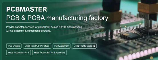
Many HDI PCB manufacturers, such as PCBMASTER, offer free DFM consultations to help clients design their PCBs with the correct specifications from the start, thereby reducing the risk of costly errors and delays during the production process.
Advantages and Disadvantages of Traditional PCBs for Cost-Effective Electronics Manufacturing
Benefits of Traditional PCBs
Lower Initial Investment Costs for Low-Volume Projects
Traditional PCBs are often the most cost-effective choice for projects with low production volumes. They use standard FR-4 materials and conventional manufacturing processes that do not require specialized equipment, making the initial setup costs significantly lower compared to HDI PCBs. For small-scale production runs, this makes traditional PCBs ideal for prototyping simple circuits or launching low-volume products without incurring high upfront expenses. For example, a small electronics startup producing 50–100 units of a consumer gadget may find traditional PCBs more economical due to lower material and tooling costs.
Simplicity in Design and Manufacturing
Traditional PCBs are also easier to design and manufacture, thanks to their simpler layer structures and larger trace widths. Most traditional boards use 2–10 layers, which reduces design complexity and simplifies the routing of electrical signals. This simplicity makes them accessible to engineers without specialized HDI expertise and ensures fewer manufacturing errors in standard circuits. Basic devices such as home appliances, remote controls, or LED lighting systems benefit from this straightforward design and production process.
Ideal Applications: Low-Cost, Low-Complexity Designs
Traditional PCBs are best suited for low-cost, low-complexity designs that do not require miniaturization, high-density interconnects, or high-frequency performance. Applications like simple IoT sensors, basic consumer electronics, and educational electronics kits are typical examples. The combination of low initial cost and simplicity makes traditional PCBs a practical choice when performance demands are modest and compact design is not critical.
Limitations of Traditional PCBs
Slower Prototyping and Extended Production Cycles
While traditional PCBs are simpler, they often suffer from longer prototyping and production cycles. Standard manufacturing processes can take 1–4 weeks for design validation and assembly, compared to 24–72 hours for Quick Turn HDI PCBs. This slower turnaround limits their usefulness in industries that require rapid iteration, such as consumer electronics startups or medical device development, where reducing time-to-market is critical.
Higher Failure Rates in Complex Designs
Traditional PCBs are less suitable for complex or high-density designs. Larger trace widths, fewer layers, and standard via sizes make it difficult to fit advanced components or manage high-frequency signals effectively. As a result, devices built on traditional PCBs may experience higher failure rates in demanding applications, especially where signal integrity and thermal management are critical, such as in automotive electronics or telecommunication systems.
Material Waste and Scalability Issues in Large-Volume Production
In large-volume production, traditional PCBs often generate more material waste due to less efficient layout and larger board sizes. Additionally, scaling production for high-volume or complex designs can be challenging because traditional PCBs lack the miniaturization and modular design features of HDI boards. This can result in higher per-unit costs and longer lead times when moving from prototyping to mass production.
Comparing Traditional vs. HDI PCBs for Specific Use Cases
Low-Volume Production vs. Mass Production
For low-volume projects (1–500 units), traditional PCBs are generally more cost-effective due to lower initial setup costs and simpler manufacturing. In contrast, Quick Turn HDI PCBs are more advantageous for high-volume production (>500 units), where their design efficiency, reduced material waste, and faster turnaround translate into significant cost savings and shorter production cycles.
Simple Circuit Designs vs. Complex, Miniaturized Designs
Traditional PCBs are ideal for simple circuits with minimal components, where large trace widths and fewer layers are sufficient. HDI PCBs excel in complex, miniaturized designs, where high-density interconnects, microvias, and multiple layers are necessary to achieve compact form factors without sacrificing performance. For example, a wearable fitness tracker or smartphone motherboard would benefit from HDI design, while a basic LED lamp controller could rely on a traditional PCB for cost-effective manufacturing.
Key Factors to Consider When Choosing Between Quick Turn HDI and Traditional PCBs
Production Volume and Cost-Effectiveness
Cost Analysis: Quick Turn HDI vs. Traditional PCBs in Low and High-Volume Production
When evaluating cost-effectiveness, production volume is a critical factor in deciding between Quick Turn HDI PCBs and traditional PCBs. For low-volume production (1–500 units), traditional PCBs are generally more economical due to lower setup costs and simpler manufacturing. In contrast, Quick Turn HDI PCBs have higher initial costs because of specialized materials, laser-drilled microvias, and advanced fabrication techniques. However, in high-volume production (>500 units), HDI boards become more cost-efficient. The reduction in material waste, fewer rework costs, and optimized layouts lower the unit cost, making HDI the preferred choice for mass production of complex electronics.
Best Use Cases for Quick Turn HDI Based on Production Scale
Quick Turn HDI is particularly advantageous for high-volume or mission-critical applications where compact design, high reliability, and advanced performance are necessary. Examples include smartphones, medical devices, automotive electronics, and telecommunication systems. Conversely, traditional PCBs are ideal for smaller-scale projects, prototypes with simple circuits, and devices where miniaturization or high-speed performance is not a priority.
Factors that Affect PCB Choice Based on Quantity
The quantity of units directly influences the return on investment (ROI) for HDI versus traditional PCBs. Small orders may not justify the higher initial costs of HDI, while larger production runs benefit from economies of scale that reduce per-unit cost. Other factors include material costs, layer count, component density, and rework potential. Companies must weigh production volume against design complexity and performance requirements to select the most cost-effective PCB solution.
Technical Design Requirements
How Miniaturization, High Frequency, and Thermal Management Affect PCB Choice
Technical specifications, such as miniaturization, high-frequency performance, and thermal management, play a decisive role in PCB selection. HDI PCBs support smaller trace widths and microvias, making them ideal for compact, high-performance designs. They also handle high-frequency signals better, minimizing signal loss and cross-talk, and provide superior thermal management through multi-layer structures and efficient component layout. Traditional PCBs, with larger traces and fewer layers, are less capable of addressing these advanced requirements.
HDI vs. Traditional PCBs for Specific Design Needs: A Comparison
Miniaturization: HDI supports dense layouts; traditional PCBs are limited.
High-frequency applications: HDI can use RF-optimized laminates; traditional PCBs may suffer signal degradation.
Thermal management: HDI enables better heat dissipation with multi-layer stacking; traditional PCBs rely on basic thermal handling.
This comparison shows that HDI is preferred for compact, high-speed, and heat-sensitive electronics, whereas traditional PCBs suffice for simple, low-speed circuits.
Advanced Features: RF Materials, Microvias, and Fine-Pitch BGAs
Advanced features like RF materials, microvias, and fine-pitch Ball Grid Arrays (BGAs) are only feasible with HDI PCBs. These features allow for high-frequency signal integrity, dense interconnections, and miniaturized component placement, which are essential in wearables, smartphones, and aerospace electronics. Traditional PCBs cannot reliably support these advanced components, limiting their suitability for complex modern designs.
Lead Time and Turnaround Expectations
How Turnaround Time Impacts Time-to-Market
Turnaround time is critical in fast-paced electronics development. Quick Turn HDI PCBs offer 24–72 hour prototyping and rapid production, enabling faster design iteration and reduced time-to-market. Traditional PCBs typically require 1–4 weeks, which may slow down product launches, especially in industries like consumer electronics or medical devices, where speed is essential for competitive advantage.
Choosing the Right PCB Solution Based on Project Urgency
Project urgency determines the preferred PCB solution. For time-sensitive prototypes or rapid product iterations, Quick Turn HDI is optimal due to fast production and flexibility in design changes. For non-urgent projects or low-volume, low-complexity devices, traditional PCBs are sufficient, offering lower costs and simpler manufacturing without sacrificing project timelines.
Practical Tips for Selecting the Right PCB Solution for Your Project
When to Choose Quick Turn HDI PCBs
Use Case Scenarios for High-Density, Miniaturized Designs
Quick Turn HDI PCBs are ideal for projects requiring compact, high-density designs. Products such as smartphones, wearables, and IoT devices often demand multiple components packed into small spaces. HDI technology, with microvias and fine-pitch traces, allows engineers to optimize circuit layouts without increasing board size, making it the preferred choice for miniaturized electronics.
When Speed and Performance Are the Top Priorities
If your project requires fast prototyping and rapid design iterations, Quick Turn HDI PCBs can significantly reduce time-to-market. The ability to produce prototypes in 24–72 hours accelerates testing, validation, and iteration cycles. This is particularly important for startups or product developers working in competitive markets, where early launch can provide a crucial advantage.
How Quick Turn HDI PCBs Benefit Mission-Critical Applications
For mission-critical applications, including medical devices, aerospace electronics, and automotive systems, Quick Turn HDI PCBs offer enhanced reliability, signal integrity, and thermal management. The multi-layer, high-density construction supports critical components and reduces failure risks. Automated inspection techniques like AOI and AXI further ensure that each PCB meets strict quality standards, providing confidence for applications where device performance and safety are non-negotiable.
When to Choose Traditional PCBs
Cost-Effective for Low-Volume, Simple Designs
Traditional PCBs are the most cost-effective solution for low-volume production or projects with simple circuits. Standard materials and conventional fabrication methods keep setup costs low, making them suitable for small batches or prototype devices where miniaturization and high-speed performance are not required.
Best for Projects with Relaxed Timeline and No Complex Design Requirements
If your project allows for longer production timelines and involves basic circuitry, traditional PCBs are a practical choice. With typical lead times of 1–4 weeks, they can accommodate projects where speed is not the primary concern. Their simplicity reduces manufacturing complexity and avoids the need for specialized HDI design expertise.
Why Traditional PCBs May Be the Better Option for Basic Circuitry
For simple, low-cost devices, traditional PCBs offer reliable performance without the expense or complexity of HDI technology. Examples include remote controls, basic LED lighting circuits, and household electronics, where large trace widths and fewer layers are sufficient. In such cases, traditional PCBs deliver functional reliability at minimal cost.
How to Optimize PCB Manufacturing with PCBMASTER’s Services
Design for Manufacturing (DFM) Support for Both HDI and Traditional PCBs
Using PCBMASTER’s DFM services ensures that your designs are optimized for manufacturability. DFM reviews highlight potential layout issues, recommend material selection, and suggest adjustments for trace routing, via placement, and layer stacking. By addressing these factors early, both HDI and traditional PCBs can achieve higher yield, fewer defects, and lower production costs.
Comprehensive PCB Selection Guide: Cost, Design, and Application Considerations
PCBMASTER provides a step-by-step selection guide that evaluates project requirements including volume, design complexity, material needs, and performance targets. This structured approach helps engineers choose the most cost-effective and technically appropriate PCB type, whether Quick Turn HDI or traditional. For instance, complex multi-layer wearable devices would benefit from HDI, while simple educational kits may use traditional PCBs.
Post-Manufacturing Inspection and Quality Assurance Services (AOI/AXI)
To ensure high-quality PCB production, PCBMASTER offers Automated Optical Inspection (AOI) and X-ray Inspection (AXI) for both HDI and traditional boards. These services detect surface defects, misaligned components, and hidden soldering issues, minimizing the risk of post-production failures. Real-time inspection results allow manufacturers to correct defects promptly, ensuring consistent reliability and product performance.
Conclusion: Choosing the Best PCB Solution for Cost-Effective Electronics Manufacturing
Choosing the right PCB solution is critical for achieving cost-effective electronics manufacturing. Quick Turn HDI PCBs offer fast prototyping, high-density design capabilities, and superior performance, making them ideal for miniaturized, high-frequency, and mission-critical applications. However, they come with higher initial setup costs and require specialized engineering expertise. Traditional PCBs, on the other hand, are simpler, more affordable for low-volume projects, and well-suited for basic circuits with relaxed timelines, but they may struggle with complex, high-density designs and extended production cycles.
The best choice depends on your project’s complexity, production volume, and performance requirements. For high-volume or compact, high-performance designs, Quick Turn HDI PCBs deliver better long-term efficiency and scalability. For low-volume, low-complexity projects, traditional PCBs remain the most practical and cost-efficient option.
By carefully evaluating these factors and leveraging services such as Design for Manufacturing (DFM) analysis and automated inspection (AOI/AXI), manufacturers can optimize cost, quality, and time-to-market. Selecting the right PCB technology ensures reliable, high-performance electronics while minimizing waste and production delays, giving businesses a competitive edge in today’s fast-paced electronics market.
FAQs
1. Why Are Quick Turn HDI PCBs More Expensive Initially Than Traditional PCBs?
Quick Turn HDI PCBs require specialized materials such as high-frequency laminates and advanced substrates, along with precision tools like laser drilling machines for creating microvias. These advanced manufacturing processes and materials drive higher upfront costs compared to traditional PCBs, which use standard FR-4 materials and conventional fabrication methods. While the initial investment is higher, HDI PCBs become cost-effective in high-volume production due to reduced material waste and faster assembly times.
2. Can Quick Turn HDI PCBs Be Used for Military or Aerospace Applications?
Yes, Quick Turn HDI PCBs are well-suited for military, aerospace, and other mission-critical applications. Their multi-layer designs, high-density interconnects, and precise signal routing provide excellent reliability, signal integrity, and thermal management. Combined with Automated Optical Inspection (AOI) and X-ray Inspection (AXI), HDI PCBs meet IPC Class 3 standards, ensuring they can perform under demanding conditions where failure is not an option.
3. What Is the Impact of Quick Turn HDI on Prototyping and Product Development Cycles?
Quick Turn HDI PCBs accelerate prototyping and product development by reducing production times from weeks to 24–72 hours for prototypes. This fast turnaround allows engineers to iterate designs quickly, test multiple revisions, and identify issues early in the development cycle. As a result, product launch timelines are shortened, enabling companies to enter the market faster and respond more effectively to customer demands.
4. What Are the Most Common Challenges When Switching from Traditional to HDI PCBs?
Switching to HDI PCBs introduces several challenges. The design complexity is higher due to microvias, finer traces, and multi-layer routing. Initial setup costs are also greater because of specialized materials and precision tools. Additionally, expert engineering knowledge is required to ensure proper layout, signal integrity, and manufacturability. Proper planning and Design for Manufacturing (DFM) reviews can help mitigate these challenges.
5. How Can I Ensure the Quality of My Quick Turn HDI PCB Orders?
Ensuring quality starts with automated inspection systems. AOI checks surface components for misalignment or soldering defects, while AXI inspects hidden solder joints and BGAs. Real-time defect detection during production allows for immediate corrections, reducing the risk of post-production failures. Choosing a manufacturer that provides these quality assurance measures helps guarantee high reliability and zero-defect delivery for HDI PCBs.

