


Key Challenges in mSAP Technology for Ultra-Fine Circuit Manufacturing
mSAP (modified Semi-Additive Process) is a cutting-edge manufacturing technology that plays a crucial role in producing ultra-fine circuit boards, which are essential for today’s high-performance electronic devices. This technology combines both additive and subtractive processes to create highly precise circuits with microvias, a key requirement for compact, high-density designs found in smartphones, AI devices, and high-performance computing (HPC) systems.
What sets mSAP apart from traditional subtractive methods is its ability to achieve extremely fine line widths and precise patterning, which are critical for applications like substrate-like PCBs (SLP). These ultra-fine circuits are vital for the latest advancements in electronic devices that need to shrink in size without compromising performance.
As the demand for smaller, faster, and more efficient electronics continues to grow, mSAP’s importance is only increasing. Technologies like AI and HPC require manufacturing methods that can meet their strict demands for circuit precision and performance. However, mSAP also faces several challenges, and in the following sections, we’ll dive into the key technical hurdles of the mSAP process, as well as the challenges involved in scaling it for large-scale production.
mSAP Process Core Technical Challenges
What Are the Core Technical Challenges in mSAP?
The mSAP process involves advanced manufacturing techniques for ultra-fine circuit boards. The core challenges are related to the precision required in every step, the high-performance equipment needed, and the significant investment required to set up the process. These challenges make mSAP a complex technology to implement and scale.
Precision: The process demands exceptional control over minute details, such as line width and copper thickness, which must be precisely maintained to avoid defects.
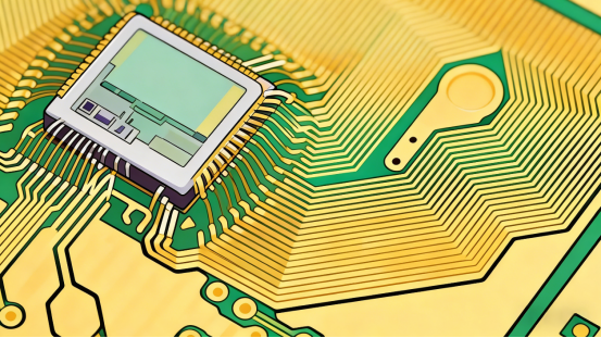
Equipment Requirements: mSAP relies on high-end machinery like laser direct imaging (LDI) for fine line patterning and continuous electroplating lines for uniform copper deposition. These machines are costly and highly specialized.
Investment Barriers: Setting up an mSAP production line requires heavy investment in both equipment and facilities, such as clean rooms and precision machinery, making it financially inaccessible for many companies.
Why Is Flash Etching a Challenge in mSAP?
Flash etching is a unique and challenging part of the mSAP process, where thin copper layers are chemically removed to form precise circuit patterns. This step is crucial but difficult to control.
Definition and Basic Steps: Flash etching involves using a chemical process to remove excess copper, leaving only the circuit traces. However, it requires extreme precision to ensure the copper traces remain intact without being eroded.
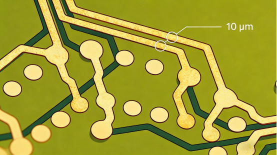
Micron-level Copper Layer Etching Control: The copper layers in mSAP are extremely thin, typically in the range of 1-3 microns. This makes it difficult to control the etching process to prevent the copper from being over-etched or unevenly removed.
Undercut Impact and Solutions: "Undercut" refers to the unwanted erosion of copper beneath the surface, which can cause lines to become too narrow, or even break, leading to poor conductivity or open circuits. To avoid this, careful monitoring of etching depth is necessary.
Precise Etch Stopping: The challenge lies in stopping the etching process at the right moment to avoid damaging the plated lines. Advanced chemical control and automated feedback systems are essential to achieve the right balance.
What Are the Technical Bottlenecks in Electroplating Control?
Electroplating is a critical step in mSAP, where copper is deposited onto the board to form the conductive paths. Several challenges exist in controlling the electroplating process.
How to Ensure Electroplating Uniformity on Large Boards?
Uniform copper deposition across large, high-density circuit boards is one of the most difficult challenges in mSAP.
Micro-level Thickness Control: Ensuring that copper is evenly plated in micro-thin layers, especially for small vias and narrow lines, is essential. Any inconsistency in thickness can cause electrical defects, such as increased resistance or short circuits.
Void Prevention: Voids are gaps or air pockets that can form during electroplating, especially in deep vias or narrow trenches. These voids disrupt the integrity of the copper layer and compromise the circuit's reliability. To avoid this, the plating process must be carefully controlled with additives that ensure full, uniform copper coverage.
What Are the Key Challenges in Electroplating Additive Mixture Ratios?
The chemistry of the electroplating solution plays a huge role in achieving high-quality results.
Additive Functionality and Mixture Ratios: Additives such as inhibitors, accelerators, and leveling agents need to be precisely balanced to ensure optimal copper plating. These chemicals help control plating speed, prevent uneven deposition, and ensure smoothness and uniformity of the copper layer.
Dynamic Filling of Holes and Surfaces: Achieving complete, uniform filling of microvias and other circuit holes is crucial. The additives help ensure that the copper deposits evenly both inside holes and on the surface, avoiding areas that are under-plated or filled with voids.
How Does Equipment Compatibility Affect Electroplating?
Advanced electroplating formulas often require specialized equipment to function correctly, which can create compatibility issues.
Dependency on Specialized Equipment: Some plating solutions need specific equipment to work effectively, such as machines with precise temperature and chemical control. This equipment can be expensive and may limit the flexibility of mSAP processes across different manufacturers.
What Are the Material and Thermal Management Challenges in mSAP?
The mSAP process requires precise control over materials and thermal conditions to maintain the integrity of ultra-fine circuits.
What Challenges Arise with Thin Substrate and Copper Foil?
The use of ultra-thin copper foil (around 1.5-3 microns) presents several difficulties in maintaining circuit quality.
Dimensional Stability and Wrinkling Resistance: Thin copper foil can easily warp or wrinkle during manufacturing, leading to defects in the circuit. This makes it essential to maintain strict control over the temperature, pressure, and handling of the foil.
How Does Thermal Stress Affect mSAP?
Thermal stress is a significant challenge for high-power electronics, especially when integrated with AI and HPC systems.
Heat Generation from High-Power Chips: Devices such as AI processors and HPC chips generate substantial heat, which can cause warping of the substrate and distortion of the fine copper traces. This can lead to performance issues like signal loss or even complete failure of the circuit.
Maintaining Stability in Thermal Cycling: Over time, repeated heating and cooling cycles can cause the fine lines created through mSAP to expand or contract, affecting their mechanical strength. Ensuring that the circuit remains stable during thermal cycling is critical, requiring careful material selection and design of the thermal management system.
How Does mSAP Rely on High-Precision Equipment?
The mSAP process depends heavily on specialized, high-precision equipment to ensure the accuracy of the manufacturing steps.
How Does Laser Direct Imaging (LDI) Apply to mSAP?
Laser Direct Imaging (LDI) is a critical technology used in the mSAP process to pattern fine lines with precision.
Precision Requirements for Fine Line Exposure: LDI uses lasers to expose photoresists and define circuit patterns. The precision of this step is crucial, as even minor errors in exposure can lead to defects in the final circuit. LDI enables the creation of ultra-fine lines, but requires expensive and sophisticated equipment.
How Does Continuous Electroplating Line Control Uniformity?
Achieving a smooth and uniform copper layer across large boards is another challenge for mSAP.
Ensuring Even Plating: Continuous electroplating lines are used to deposit copper onto the entire board. The process must be precisely controlled to ensure the copper layer is consistent, especially in areas with fine patterns and deep vias. Any variation in thickness can affect the electrical performance of the circuit.
Challenges in mSAP Implementation and Mass Production
Why Is mSAP Difficult to Implement and Requires High Equipment Investment?
mSAP technology, while offering significant advantages in producing ultra-fine circuits, faces major barriers when it comes to implementation and scaling for mass production. The primary challenges stem from the high cost of necessary equipment, facility upgrades, and the long-term financial commitment required.
High Equipment Investment and Facility Requirements
mSAP relies on specialized machinery that is both expensive and highly advanced. Key equipment includes laser direct imaging (LDI) systems for precise patterning and continuous electroplating lines to ensure uniform copper deposition. Additionally, mSAP production requires controlled environments, such as clean rooms, to maintain the precision of the process and prevent contamination.
Setting up these facilities not only requires substantial capital investment but also continuous maintenance and updates to keep up with technological advancements. For example, manufacturers need to build custom electroplating tanks, integrate complex chemical delivery systems, and ensure proper airflow and temperature control. These costs can be prohibitive for smaller companies or those with limited resources, making it difficult for new players to enter the market.
Long Cycle and High Investment Risk
The investment in mSAP technology does not offer immediate returns. Establishing a fully functional mSAP production line involves a long setup time, from acquiring equipment to training personnel and refining processes. Even once the system is operational, it may take months or years to fully optimize production processes and achieve consistent yields.
The long return on investment (ROI) cycle is a significant risk for companies. The market for mSAP is still niche, with high-volume applications limited to top-tier electronics like high-end smartphones, AI systems, and HPC devices. Given these uncertainties, businesses must carefully assess whether the investment will generate the desired returns, or if a more cost-effective production method (like traditional subtractive processes) would be a better alternative.
How to Balance mSAP Market Demand and Cost Pressures?
Despite its potential, the mSAP technology faces constant pressure to balance the high production costs with the actual market demand. This balancing act is crucial for companies looking to adopt mSAP on a larger scale.
High-Cost Technology and Market Limitations
mSAP’s high production costs, driven by expensive equipment, materials, and facility requirements, limit its applicability to high-end electronics. These high costs are justified by the superior performance and precision of the technology, but only in products where performance, miniaturization, and circuit density are non-negotiable.
For example, major tech companies like Apple and Samsung rely on mSAP to meet the needs of their flagship devices, where space is limited, and circuit density is critical. However, for lower-end consumer electronics, such as basic smartphones or home appliances, traditional manufacturing methods like HDI (High-Density Interconnect) boards are sufficient and much cheaper. As a result, mSAP is typically reserved for a small segment of the market, limiting its broader application.
Market Capacity and Application Scenarios
The demand for mSAP is primarily driven by a few specific sectors, particularly high-performance computing (HPC), AI, and advanced consumer electronics like smartphones and wearables. These industries require ultra-fine, high-performance circuits that mSAP can deliver. However, the overall market for mSAP is still limited, with many other applications falling outside its niche.
The potential for mSAP to reach mass-market adoption is constrained by this limited application base. For industries with less stringent performance requirements, traditional PCB manufacturing methods remain adequate and cost-effective. This market concentration means that mSAP’s scalability is inherently limited, and it may struggle to penetrate more cost-sensitive sectors.
How Do Talent and Technical Barriers Affect mSAP Adoption?
mSAP technology involves multiple disciplines, including chemistry, materials science, and precision engineering. The complexity of these areas presents significant technical and talent barriers for companies looking to adopt or develop mSAP capabilities.
Cross-Disciplinary Technical Knowledge Challenges
mSAP requires expertise in various fields, including chemical processes for electroplating, material selection for ultra-thin substrates, and advanced mechanical engineering for equipment design. This interdisciplinary knowledge is crucial to successfully implementing and optimizing mSAP processes.
For example, understanding the behavior of specific chemicals in electroplating solutions, or knowing how to prevent substrate warping during the heating and cooling cycles, requires a deep understanding of both material science and chemistry. Without access to experts in these fields, companies may struggle to refine their mSAP processes and achieve high yields, further increasing the cost and complexity of adoption.
High Technical Barriers and Talent Shortage
The specialized knowledge required for mSAP creates significant entry barriers for new players. Established companies in the PCB manufacturing space often have teams of experts who have spent years developing their knowledge of these processes. New entrants may face difficulties in recruiting the necessary talent, further slowing the adoption of mSAP.
The talent shortage extends beyond chemical engineers and material scientists to also include experienced operators and technicians familiar with high-precision manufacturing equipment. Without access to this skilled workforce, companies may experience delays in mSAP implementation and face quality control challenges as they scale production.
Future Prospects and Application Expansion of mSAP
How Are AI, HPC, and Advanced Packaging Technologies Driving mSAP’s Application Expansion?
The growth of AI, high-performance computing (HPC), and advanced packaging technologies is fueling the demand for more efficient and compact circuit board manufacturing. mSAP plays a pivotal role in addressing these needs, offering the precision and performance required for cutting-edge electronics.
Demand for High-Performance Computing and Ultra-Small Form Factors
HPC and AI applications require powerful, compact devices that can process vast amounts of data quickly. These systems often need circuits with extremely fine line widths and high-density interconnections to maximize performance in a small form factor. mSAP is well-suited for this task, as it allows manufacturers to produce ultra-fine, high-density circuit boards that fit into the compact spaces demanded by modern AI processors and HPC devices.
For example, AI chips and HPC systems used in data centers require high-bandwidth interconnects, which can only be achieved with precise, small-pitch traces. mSAP enables the creation of such fine circuits, making it the go-to solution for these high-performance applications.
Overcoming Current Technological Bottlenecks to Expand Applications
Currently, mSAP is limited by several technological challenges, including its high cost, reliance on specialized equipment, and difficulty achieving perfect uniformity across large boards. To expand mSAP's application in broader markets, these bottlenecks must be addressed.
Process Optimization: Improvements in chemical formulations and process automation can reduce the cost and complexity of mSAP. By optimizing the electroplating and etching processes, manufacturers can achieve better yield rates and reduce defects, making mSAP more viable for large-scale production.
Cost Reduction: Advances in equipment and material costs can help bring down the overall expenses of mSAP manufacturing. As more companies invest in scaling the technology, economies of scale will likely reduce costs, allowing mSAP to be adopted for applications beyond high-end electronics.
By addressing these challenges, mSAP could find its place in a wider array of industries, including automotive electronics, IoT devices, and consumer electronics, which increasingly require smaller, more efficient circuit boards.
What Is the Future Development Direction of mSAP Technology?
As the demand for smaller, faster, and more powerful electronics grows, mSAP technology is evolving to meet these needs. Future development trends include process optimization, innovation in materials, and new equipment advancements, all of which will help expand mSAP's capabilities.
Process Optimization and Innovation Trends
One of the key areas of focus for mSAP's future is the continued optimization of manufacturing processes. This includes refining the balance between additive and subtractive steps to achieve higher yield rates, better precision, and faster production times. Innovations such as advanced patterning techniques and more efficient etching methods could help mSAP meet the growing demands for even finer, more densely packed circuits.
Furthermore, automating parts of the mSAP process, such as electroplating and inspection, can speed up production and reduce human error. These optimizations will make mSAP more efficient and cost-effective, paving the way for broader adoption.
The Potential of New Materials and Equipment Development
The development of new materials and equipment will also play a crucial role in the future of mSAP. For example, the introduction of more advanced, high-performance materials that can withstand higher temperatures or provide better electrical properties will open up new applications for mSAP, especially in industries like automotive and aerospace.
Materials: The exploration of new copper alloys, thin-film materials, and more efficient plating solutions could improve the performance and durability of mSAP circuits. For instance, advanced copper-clad laminates that offer better thermal conductivity and resistance to wear could enhance mSAP's reliability, especially in high-power applications.
Equipment: Innovations in precision equipment, such as laser direct imaging (LDI) systems and automated inspection tools, will make it easier to achieve the fine line resolutions required for mSAP. Additionally, new developments in electroplating technology could allow for more efficient and uniform deposition of copper, improving the overall quality of the final product.
By embracing these advancements, mSAP could become even more adaptable, enabling it to meet the diverse needs of modern electronic devices and industries.
Conclusion
While mSAP technology offers significant advantages in producing ultra-fine, high-performance circuits, it faces several key challenges. These include the complexity of the manufacturing process, the high cost of specialized equipment, and the technical barriers related to precision control, such as flash etching and electroplating uniformity. Additionally, mSAP's application is currently limited to high-end electronics due to its high costs and market constraints.
However, as demand for smaller, faster, and more powerful electronic devices continues to grow, mSAP's potential is expanding. Advances in process optimization, new materials, and better equipment are set to overcome these challenges, opening up new application areas in industries like AI, HPC, and advanced packaging.
For companies looking to adopt mSAP technology, partnering with experienced PCB manufacturers like PCBMASTER is key. With years of expertise in PCB production, PCBMASTER consistently delivers high-quality, reliable solutions to meet the evolving needs of the electronics industry. Their commitment to innovation and precision ensures that customers receive the best possible products, whether for mSAP or other advanced manufacturing processes.
FAQs
What Are the Key Differences Between mSAP and Traditional Subtractive Processes?
Aspect mSAP Traditional Subtractive Process Manufacturing Precision Extremely fine line widths and high-density circuits are possible (down to micron levels) Limited to larger line widths and less fine detail Cost High due to specialized equipment, materials, and facility requirements Generally lower as it relies on standard equipment and materials Application Best suited for high-performance, ultra-fine circuit boards like SLP, advanced packaging, and high-end electronics Suitable for standard PCBs with larger traces, used in lower-end electronics Process Complexity More complex, involving both additive and subtractive processes Simpler, involving only subtractive etching methods Material Requirements Uses ultra-thin copper foil and specialized materials Uses standard copper foil and fewer specialized materials
Why Is mSAP Particularly Suitable for Substrate-Like PCBs (SLP) Manufacturing?
mSAP is ideal for Substrate-Like PCB (SLP) manufacturing because it enables the creation of ultra-fine and precise circuits, which are essential for the compact, high-density designs required in SLP applications. SLPs are used in high-performance electronics such as smartphones, AI processors, and advanced consumer devices, where space is limited and circuit density is crucial.
High Precision: mSAP allows manufacturers to achieve extremely fine traces and microvias, which are essential for meeting the stringent requirements of SLPs.
Enhanced Performance: The precise circuit design and minimal signal loss in mSAP-based SLPs contribute to better performance in high-speed applications.
Miniaturization: The ability to create smaller and denser circuits supports the ongoing trend of miniaturization in electronics.
What High-Precision Equipment Does mSAP Require?
mSAP requires several key pieces of high-precision equipment to achieve its fine manufacturing standards:
Laser Direct Imaging (LDI): LDI systems are used for precise exposure of photoresists, allowing for the creation of ultra-fine circuit patterns. LDI ensures that the high-density interconnects needed for applications like SLPs are accurately formed.
Continuous Electroplating Lines: These are used to achieve uniform copper deposition on the PCB surface, particularly important for microvias and small traces. The plating process must be uniform to prevent defects such as voids or uneven thickness.
Chemical Processing Systems: Specialized systems are required to manage the chemicals used in the etching and plating processes, ensuring precise control over the thickness of copper layers and preventing defects.
Will the High Cost of mSAP Technology Affect Its Widespread Adoption?
Yes, the high cost of mSAP technology could limit its widespread adoption. The substantial investment required for specialized equipment, cleanroom facilities, and advanced materials makes it financially prohibitive for many companies. However, as the demand for ultra-fine, high-density circuits grows in industries like AI, HPC, and mobile devices, the market for mSAP is expected to expand.
High-Value Applications: mSAP is particularly suited for high-end electronics, where the need for miniaturization, high-speed processing, and performance outweigh the high manufacturing costs. This includes sectors like mobile devices, high-performance computing, and AI.
Economies of Scale: As more companies adopt mSAP and as the technology advances, economies of scale may drive down the cost of production, making it more accessible for broader use.
How Are Thermal Management Challenges in mSAP Addressed?
Thermal management is a critical issue for mSAP, particularly in high-power applications like AI chips and high-performance processors, which generate substantial heat. Excessive heat can cause warping, signal degradation, or failure in the fine circuits formed through mSAP.
High-Power Chips and Heat Generation: AI processors and HPC systems generate significant amounts of heat, which can affect the stability of the circuits. The copper traces and substrates in mSAP need to maintain their structural integrity even when exposed to thermal cycling.
Solutions: Advanced thermal management solutions, such as the use of high-performance thermal materials in PCBs, are used to dissipate heat effectively. Additionally, heat spreaders and improved substrate designs help maintain temperature stability and prevent warping.
Material Innovations: The use of materials with better thermal conductivity, such as specialized copper alloys or ceramic-based substrates, can also help manage the heat generated by high-power chips, ensuring the mSAP circuits remain stable over time.
By addressing these thermal challenges, mSAP can continue to be used effectively in high-performance, heat-sensitive applications.
Author Bio
Hi, I'm Carol, the Overseas Marketing Manager at PCBMASTER, where I focus on expanding international markets and researching PCB and PCBA solutions. Since 2020, I've been deeply involved in helping our company collaborate with global clients, addressing their technical and production needs in the PCB and PCBA sectors. Over these years, I've gained extensive experience and developed a deeper understanding of industry trends, challenges, and technological innovations.
Outside of work, I'm passionate about writing and enjoy sharing industry insights, market developments, and practical tips through my blog. I hope my posts can help you better understand the PCB and PCBA industries and maybe even offer some valuable takeaways. Of course, if you have any thoughts or questions, feel free to leave a comment below—I'd love to hear from you and discuss further!

