


PCB Drill Step Deep Control A Technical Game Where Millimeters Determine Success or Failure
Introduction
In the world of high-speed PCBs, a deviation of even a fraction of a millimeter can determine the fate of a signal. High speed design is a critical factor in modern electronics, where maintaining signal integrity is paramount.
In high-speed digital circuit and RF circuit design, each via on a PCB in printed circuit boards is no longer just a simple electrical connection point. When signal rates reach 5G, 10G, or even higher, the seemingly insignificant metal stubs hidden within the vias can become fatal killers of signal integrity.
These via stubs can disrupt the signal path, causing reflections and signal loss that degrade overall performance. Back drilling is important because it removes these unused stub portions, helping to maintain a clean and efficient signal path for optimal signal integrity.
This is where back drilling technology takes the stage, and the precision of depth control becomes the core and key of this technology.
What is PCB Back Drilling? Why is Depth Control So Critical?
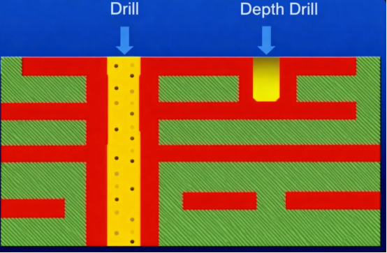
PCB back drilling, as the name suggests, is a step within the pcb manufacturing process that involves a secondary drilling operation on already completed vias to remove unwanted metal stubs. These excess stubs are found inside the drill holes and act like small antennas, causing signal reflection, loss, and crosstalk, severely degrading high-speed signal integrity.
The core challenge in back drilling depth control lies in: Drilling too shallow leaves excessive stub residue in the drill holes, failing to improve signal quality; drilling too deep during the drilling operation may penetrate the target inner layer circuits, causing open or short circuits. It is this precise control within millimeters or even micrometers that determines the final performance and yield rate of the PCB.
Drilled Holes and Via Stubs: The Hidden Obstacles to Signal Integrity
In the intricate world of printed circuit board (PCB) manufacturing, drilled holes and via stubs are both essential and potentially problematic. The drilling process in PCB manufacturing is responsible for creating precise holes—known as vias—that connect copper layers and enable complex signal paths across multiple PCB layers. However, not all portions of these drilled holes are used for electrical connectivity. The unused portions, or via stubs, can become hidden obstacles that undermine signal integrity, especially in high-speed signal paths.
When high-speed signals traverse a via, any unused portion of the drilled hole acts as a stub, reflecting signals back along the path and causing signal integrity issues such as signal reflections, loss, and crosstalk. These effects are particularly pronounced in modern electronic devices where high speed signals are the norm, and even a small residual stub can degrade overall signal quality.
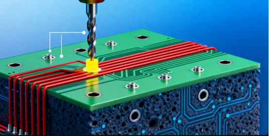
To address these challenges, the back drilling process—also known as controlled depth drilling (CDD)—is employed. This technique involves using a slightly larger drill bit to re-enter the existing via and remove the unused portion, or stub, without damaging the required target layer thickness. By carefully controlling the drill depth, the back drilling process eliminates the unwanted copper barrel that would otherwise act as an antenna, thus minimizing signal reflections and improving signal integrity.
The effectiveness of back drilling relies on meticulous planning and execution. The drill layer pair column in the drill table is used to specify which layers require back drilling, ensuring that the drilling stops precisely at the required target layer. Accurate thickness calculations are essential to avoid damaging adjacent copper layers or leaving excessive stub length. Specialized drilling equipment, such as high-precision mechanical drills or advanced laser drilling machines, is used to create precise holes with the exact depth required. The choice between mechanical drilling and laser drilling depends on the specific requirements of the PCB design and the complexity of the layer stack.
During the back drilling process, a slightly larger drill or drill bit is selected to ensure that the unused portion of the via is completely removed, while maintaining the integrity of the connected layer. This controlled depth drilling technique is critical for high speed signal paths, as it minimizes the risk of signal integrity issues and ensures reliable performance in demanding applications.
As PCB designs become more complex and the demand for high-speed electronic devices continues to rise, the importance of controlled depth drilling in PCB manufacturing cannot be overstated. By leveraging advanced drilling technology, precise hole sizing, and careful process control, manufacturers can effectively eliminate the hidden obstacles posed by via stubs, ensuring optimal signal quality and the success of high-speed PCB designs.
Comprehensive Analysis of the PCB Back Drilling Controlled Depth Drilling Process
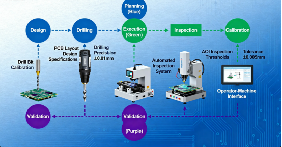
Design Phase: The Foundation Establishing Depth Benchmarks
The first step in back drilling depth control begins with precise design definition, often using the Layer Stack Manager to define the start and stop layers for back drilling. Designers must clarify:
Back Drilling Depth = (Total PCB Thickness - Thickness from Termination Layer to Bottom) ± Process Compensation Value
When calculating the back drilling depth, it is important to consider the thickness target layer to ensure the correct depth is achieved and to maintain structural integrity.
For example, for a PCB with total thickness of 1.6mm requiring removal of stubs from surface layer (L1) to L5 (preserving conduction from L1 to L5, removing the portion from L5 to bottom layer L10), the back drilling depth should be “thickness from L1 to L5 + 0.05mm compensation” to avoid damaging L5.
In design documents, specifying which layers require back drilling is done by defining drill layer pairs and documenting them using a placed drill table. The “target depth” and “allowable tolerance” for back drilling must be clearly marked—typically requiring ±0.05mm, with stricter ±0.025mm for high-frequency boards.
Meanwhile, design conflicts must be avoided during the design phase. Back drilling positions should avoid dense inner layer circuits or copper, reserving ≥0.1mm safety distance (interlayer dielectric) to prevent inner layer penetration due to depth deviation.
Equipment Selection: High-Precision Drilling Machines as Fundamental Guarantees
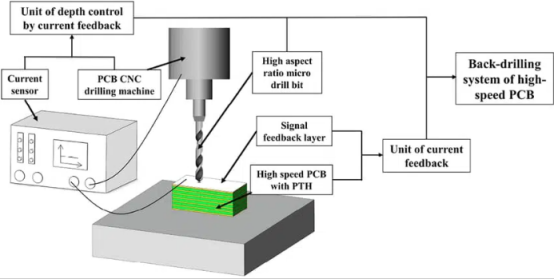
Back drilling imposes far higher requirements on equipment than conventional drilling in terms of Z-axis positioning accuracy, rotational speed stability, and depth feedback capability. Advanced drill machines are essential for achieving the precise hole depths and minimizing stub length required in high-speed PCB manufacturing. The use of specialized equipment, including high-precision drill machines, is critical for meeting these stringent requirements:
·Z-axis positioning accuracy: ≤±0.01mm, ensuring minimal linear error in drill tip descent depth
·Closed-loop depth control system: Equipped with optical encoders or laser displacement sensors to monitor drill tip position in real time and dynamically correct depth
·Spindle stability: Spindle radial runout ≤0.002mm, preventing drill tip offset causing inaccurate depth measurement
·Optical alignment function: Using CCD to identify panel edge locating holes or Mark points, compensating for PCB expansion and contraction
For instance, the “Drilling Depth Control Method” patent recently disclosed by Han’s CNC uses the abutment surface of the first or second pressure foot in the pressure foot module against an equal-height component to obtain the first height value of the spindle, then controls the tool movement to the tool detector to obtain the second height value of the spindle and tool length, thus achieving precise depth control.
Process Parameters: Matching Material and Drill Bit Characteristics
Process parameter settings must balance the core requirements of “drilling through stubs” and “not damaging inner layers”:
·Feed rate: Optimized for different board materials and drill bit diameters, with careful consideration of the required drill diameter and back drill diameter for effective stub removal.
·Spindle speed: Key factor affecting drilling quality and drill bit life
·Retraction speed: Proper setting prevents hole wall damage
·Hole size: The specified hole size directly influences the selection of drill diameter and back drill diameter, ensuring proper copper removal and signal integrity.
For thick board back drilling (≥3mm), a “step back drilling” strategy can be adopted—this is one of several drilling plays used in PCB manufacturing. Step back drilling involves first drilling to a shallow depth (e.g., target depth 2mm, drilled in two steps of 1mm each), reducing stress deformation from single drilling and allowing precise control over stub length.
For multilayer heterogeneous materials (such as PCBs containing ceramic or metal cores), segmented parameter settings are needed for different materials (e.g., reducing feed rate by 50% when drilling through ceramic layers) to prevent depth jumps caused by sudden changes in cutting resistance. Different drilling plays may be employed to optimize performance and maintain high-speed signal integrity.
Calibration and Compensation: The Essence of Eliminating Systematic Errors
1. Drill Bit Length CalibrationAfter new drill bit installation or replacement, use a “drill bit length measuring instrument” (accuracy ±0.001mm) to measure actual length, compare with theoretical value, and input compensation into the system. Example: theoretical length 50mm, measured 49.98mm, compensation -0.02mm.
Recheck required after every 500-1000 holes, especially for micro-diameter drill bits that wear more rapidly.
2. PCB Thickness Pre-measurementSame-batch PCBs may have ±0.05mm thickness variations due to lamination errors. Use a micrometer to measure actual board thickness at multiple points (≥3 points) near back drilling areas, take average value to correct back drilling depth. When calibrating, also account for the 'thickness stub remainder' as a tolerance parameter to ensure the final layer thickness after processing meets the required specification.
3. Drill Tip Wear CompensationDrill tip wear causes “effective cutting depth” reduction (e.g., wear of 0.03mm reduces actual depth by 0.03mm). This can be addressed through “count-based compensation” (automatically increasing depth by 0.01mm after every N holes) or “image recognition” (camera detecting drill tip wear amount, dynamic compensation).
Process Monitoring and Inspection: The Final Checkpoint for Verifying Depth Accuracy
For real-time monitoring, use “contact depth sensing”: when drill tip contacts PCB surface, sensor triggers “depth starting point,” continuously records drill tip descent distance, automatically stops and alarms when exceeding target depth ±0.03mm.
Off-line inspection includes:
·Cross-section analysis: Perform metallographic sectioning on first-article PCB back drilling positions, use microscope to measure stub residual length (requirement ≤0.05mm) and distance from back drilling bottom to inner layer (must be ≥0.03mm to avoid penetration). It is crucial to verify the quality and dimensions of drilled vias during this process to ensure compliance with manufacturing standards.
·X-Ray inspection: Use X-Ray back drilling areas, observe whether hole bottom aligns with target inner layer, calculate depth deviation (suitable for batch sampling, more efficient than cross-sectioning). X-Ray inspection also helps confirm the setup and effectiveness of drilled vias, ensuring proper layer configuration and via properties.
·Impedance testing: For high-frequency signal vias, use impedance analyzer to measure impedance after back drilling (e.g., target 50Ω, deviation must be ≤±5Ω), indirectly verifying whether stub residue meets standards and assessing the impact of drilled vias on signal integrity.
Depth Control Strategies for Special Application Scenarios
Back Drilling Challenges in Flexible PCBs
Flexible PCBs present additional challenges for back drilling depth control due to their unique material properties. Flexible PCBs typically use polyimide as substrate material, with flexibility and thermal expansion coefficient different from conventional FR-4 materials.
When designing back drilling processes for flexible PCBs, note:
·Additional thickness measurements: More measurement points needed in different areas due to material deformation susceptibility
·Feed rate adjustments: Typically require reduced feed rates to prevent material tearing
·Dedicated backing board usage: Ensures material stability during drilling process
Depth Control in High-Frequency High-Speed Applications
For applications like 5G base stations and server motherboards, back drilling depth deviation must be controlled within ±0.025mm, requiring higher precision equipment (such as imported high-precision drilling machines) and stricter inspection methods. In these high-speed, high-frequency designs, blind vias are often used as an alternative technique to minimize stubs when back drilling is impractical or too costly, especially in high-density multilayer PCBs.
For example, a new PCB factory in Zhuhai uses German imported equipment, capable of precisely controlling back drilling STUB to 1-5 mil, meeting stringent stub requirements for high-speed PCBs. Layer-specific depth control is achieved by targeting the exact signal layer, which is critical for maintaining signal integrity. During inspection and validation, analysis of signal layer usage results is performed to assess the effectiveness of back drilling and ensure optimal signal quality.
Conclusion: Full-Process Coordination is Key to Achieving Precise Depth Control
PCB back drilling depth control is not a single-step task, but requires full-process coordinated management through "design defining benchmarks → equipment ensuring precision → parameters matching materials → calibration eliminating errors → inspection verifying results".
The core is reducing the impact of three major variables: "equipment error, material fluctuation, and drill bit wear."
As electronic equipment develops toward higher speeds and frequencies, requirements for PCB back drilling depth control will only become more stringent. Mastering the full-process key technologies of depth control can not only enhance product performance but also significantly improve production yield and reduce costs.
In this field where success or failure is determined by millimeters or even micrometers, precise depth control has become one of the core competencies of PCB manufacturing enterprises.
FAQs
Q.What is Drill Step Depth Control?
A. It refers to the process of precisely controlling multiple depth steps at the same hole position in PCB step drilling. The core objective is to maintain depth deviation within ±0.01mm to ±0.02mm, ensuring via conductivity and component compatibility.
Q.Why is Drill Step Depth Control necessary?
A. It directly impacts PCB yield (drilling errors account for 22% of defects), is a mandatory requirement in industries like automotive (IATF 16949) and medical (ISO 13485), and is a prerequisite for the mass production of miniaturized, high-density PCBs.
Q. What are the depth tolerance requirements for different scenarios?
A.
·Consumer electronics (e.g., mobile phones): ±0.02mm
·Automotive electronics: ±0.01mm
·Medical/Aerospace: ±0.008mm–±0.01mm
·Standard depth-controlled slots: ±0.05mm–±0.10mm
Q. What factors cause depth deviation?
A.
·Substrate: FR-4 resin content variation, PI stretching, abrasiveness of Rogers substrates
·Tools: Drill bit wear (e.g., carbide drills for FR-4 require replacement after ~800 holes)
·Environment: Temperature and humidity changes (FR-4 expands 0.001mm per °C)
·Operation: Parameter input errors, missed calibrations
Q. How to address deviation caused by drill bit wear?
A. Use TiAlN-coated carbide drill bits, replace based on hole count (e.g., 800 holes for FR-4, 500 for Rogers), and pair with automatic tool changers on closed-loop equipment.
Q. Are there special requirements for depth control in Flexible PCBs (FPC)?
A. Yes: Reduce drilling pressure to prevent PI stretching, store in low-humidity environments (35% RH), and measure thickness individually before drilling to adjust parameters.
Q. What is the core equipment for improving control accuracy?
A. Prioritize closed-loop CNC drilling machines, which use real-time sensors to monitor position (100+ times per second) and auto-adjust parameters if deviations exceed 0.005mm.
Q. Is the investment cost high? How long is the payback period?
A.
·Closed-loop equipment: $50,000–$200,000
·Laser depth measuring instruments: $5,000–$15,000
·Payback typically achieved in 3–6 months, or as fast as 21 days in high-scrap ·scenarios (e.g., automotive PCBs).
Q. How to demonstrate control capability to customers/auditors?
A. Retain three types of records:
·Pre-production laser/X-ray inspection data
·SPC depth trend charts
·Drill bit replacement logs
Q. How to troubleshoot insufficient or excessive drilling depth?
A.
·Insufficient Depth: Check if substrate thickness exceeds expectations, if the drill bit is improperly seated, or if depth stop settings are incorrect.
·Excessive Depth: Investigate whether humidity exceeds limits (>60% RH), drill bit wear, or excessive pressure parameters.
Author: Jack Wang

