


Essential Insights on Gold Finger in PCB Design and Application
Introduction
In personal computers, when you insert a graphics card into the motherboard, those rows of golden connection points are precisely what ensure high-quality image transmission—this is the essence of gold finger technology. These gold-plated contact edges, known as pcb gold fingers, are found on pcb boards and serve as the interface for external connections, enabling seamless communication between printed circuit boards and external hardware devices.
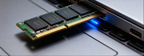
In today’s electronic products, we almost always encounter various pluggable devices: memory modules, graphics cards, expansion cards, etc. The stable connection of these devices relies on a key core technology—Gold Fingers. Pcb gold fingers are critical for connecting peripheral devices and ensuring reliable external connections in various electronic devices, such as monitors, microphones, and printers.
These golden conductive contacts arranged along the edge of circuit boards are not only bridges for physical connections but also precision structures that ensure signal integrity and power stability. In the electronics industries, pcb gold fingers play a vital role in constant pcb usage, supporting the reliability and performance of printed circuit boards across a wide range of applications.
What Are Gold Fingers? The "Golden Bridges" of Electronic Connection
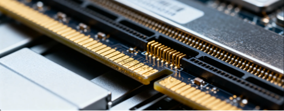
Gold fingers are not literally “pure gold fingers,” but rather a figurative term for the series of golden conductive contacts at the edge of a PCB (Printed Circuit Board). Their English name is Gold Fingers or Edge Connector. These gold plated connectors are located at the board's edge, serving as critical interconnection points for digital signals between circuit boards and devices.
The reason these contacts appear golden is because their surface is plated with a special metallic material.
·The core structure of gold fingers is a composite plating design, typically consisting of three critical layers:
·Base Layer: Copper foil substrate (thickness 35-70μm), forming conductive strips 0.3-0.8mm wide through etching
·Transition Plating Layer: Electroless nickel plating (3-5μm), preventing copper-gold interdiffusion while enhancing mechanical strength
·Surface Plating Layer: Electroplated hard gold (gold-cobalt alloy, cobalt content 0.1-0.3%), with thickness ranging from 0.05-0.1μm (ordinary consumer electronics) to 0.76μm (military grade)
Gold finger specifications, including the thickness and composition of the gold plated connector edges and contact edges, are defined by standards set by the association connecting electronics industries (IPC) to ensure quality and consistency in pcb gold finger manufacturing.
This meticulously designed structure gives gold fingers three core characteristics:
·Low Contact Resistance: Surface roughness < 0.3μm, contact resistance < 20mΩ, ensuring signal transmission integrity
·High Durability: Withstands 5,000-10,000 insertion-extraction cycles (PCIe slot standard requires ≥2,500 cycles)
·Environmental Stability: Salt spray resistance exceeds 96 hours (ASTM B117 standard), with oxidation resistance far surpassing tin, silver and other materials
The use of edge connectors and careful pcb gold finger design is essential for reliable digital signal transmission and robust electrical connectivity in modern electronic devices.
Precision Design of PCB Gold Fingers: Details Determine Success
Precise Control of Geometric Dimensions
The dimensional design of gold fingers directly affects connection reliability:
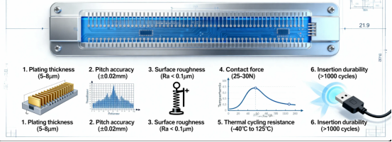
·Width: Common sizes 0.635mm, 1.27mm, must match mating interfaces (e.g., DDR5 memory gold finger width 0.8mm), with deviation controlled within ±0.02mm
·Length: Designed according to insertion depth (typically 10-20mm), effective contact length must be ≥8mm to ensure stable conduction. Note: Plating thickness is often specified in precise ranges such as one and two microns or three and six microns, depending on application requirements.
·Pitch: Adjacent gold finger spacing mostly 0.635mm, 1.27mm, minimum pitch can reach 0.3mm (high-density interfaces), with pitch deviation ≤±0.01mm to prevent short circuits
Critical Role of Edge Bevel Design
The front edges of gold fingers must be beveled, which is crucial for ensuring smooth insertion and extraction. This process, known as pcb gold finger beveling, involves slanting the pcb edge at a specified angle to enhance durability, facilitate easier mating with slots, and ensure proper electrical connection.
·Angle Selection: Typically 30° and 45° options, 30° bevel compared to 45° bevel allows easier insertion and extraction, recommended as priority. Gold fingers should always be oriented in the opposite direction from the middle of the board to ensure proper alignment and contact.
·Bevel Length: Typically in the range of 0.5-1mm
·Design Purpose: Guides insertion and extraction, preventing sharp edges from scratching mating interfaces
Excessive bevel depth will prevent gold fingers from making good contact with matching equipment during assembly, affecting performance.
Surface Treatment of Gold Finger Areas
Solder mask must be opened at gold finger areas; no ink is allowed. Solder masks and screen printing should be kept at a safe distance from gold finger areas, along with plated pads, plated holes, plated through holes, and through holes, to prevent interference, defects, and ensure mechanical strength. If ink is present, it will affect flatness, and after multiple insertion-extraction cycles, the ink will wear off and fall into the slot, causing connectivity issues. Additionally, the inner layers at the edge must be copper free to ensure proper gold plating and prevent corrosion.
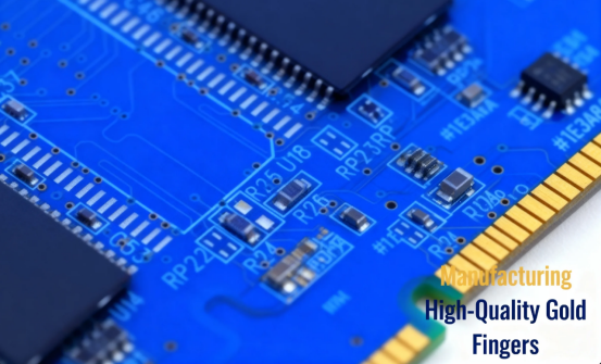
Manufacturing Process of Gold Fingers: Precision Plating Technology
Gold finger manufacturing requires three core stages:
The process begins with careful planning and design, where adherence to pcb production and pcb assembly standards is crucial to ensure the reliability and performance of the final product.
During the plating stage, it is essential to control the chemical composition of the gold alloy, particularly the cobalt and nickel content, to achieve maximum rigidity and durability. Care must also be taken to avoid excess plating, as over-application of gold or nickel can result in defects such as uneven surfaces or poor adhesion, compromising the mechanical strength and reliability of the gold fingers. Achieving an optimal surface finish, such as ENIG or gold plating, is vital for ensuring solderability, corrosion resistance, and electrical connectivity of the PCB contacts.
Pre-treatment: Substrate Activation and Cleaning
·Degreasing: Alkaline degreasing agent immersion at 50-60°C for 5-8 minutes to remove surface oils from copper foil
·Acid Cleaning: 10%-15% dilute sulfuric acid immersion at room temperature for 3-5 minutes to remove copper oxide layer
·Micro-etching: Ammonium persulfate solution treatment for 1-2 minutes to create micro-rough surface on copper, increasing contact area between plating and substrate
Plating Deposition: Critical Process Selection
Two common gold plating processes for gold fingers, selected according to application scenarios:
ENIG (Electroless Nickel Immersion Gold)
Principle: Gold layer deposited on copper surface through chemical reduction reaction, no external power supply needed
·Advantages: Low cost, excellent plating uniformity (thickness deviation ≤±10%), suitable for complex-shaped gold fingers
·Disadvantages: Poor wear resistance, hardness ≤80HV, suitable for scenarios with ≤500 insertion-extraction cycles
·Nickel immersion gold ENIG is a common surface finish for PCB gold fingers, offering good surface resistance and reliable electrical connections, but it is more susceptible to abrasive effects compared to harder gold plating methods.
Electroplating Gold
·Principle: Direct current applied through power supply to cause directional deposition of gold ions on copper surface
·Can be divided into soft gold (pure gold plating) and hard gold (alloy plating)
·Hard gold adds nickel, cobalt and other elements, hardness up to 120-200HV, wear resistance improved 3-5 times, insertion-extraction cycles ≥5,000
Electroplate gold and electroplated gold are widely used for gold fingers to achieve boosted surface resistance and enhanced durability, making them ideal for high-reliability applications where surface resistance and resistance to abrasive effects are critical.
Post-treatment: Key to Quality Assurance
·Cleaning: Multi-stage (3-5 stages) rinsing with deionized water to remove residual plating solution
·Drying: Drying in 60-80°C hot air circulation oven for 10-15 minutes to prevent plating oxidation
·Inspection: X-ray fluorescence thickness gauge for plating thickness inspection, metallographic microscope for plating integrity observation. A tape test is performed to assess the adhesion of the gold plating, while a visual test using a magnifying lens checks for surface quality, defects, and proper alignment of the gold fingers.
Application Scenarios of Gold Fingers: From Consumer Electronics to High-End Fields
High-Speed Data Transmission Fields
·Graphics Card Interfaces: PCIe x16 gold fingers contain 164 contacts, transmission rate up to 256GB/s (PCIe 5.0 standard)
·Memory Slots: DDR5 memory module gold fingers use curved design (center protrusion 0.1mm) to improve high-frequency signal integrity
·Storage Devices: M.2 SSD interface gold fingers with plating thickness up to 0.15μm, meeting 15W power transmission requirements
Industrial and Special Environments
In industrial and special environments, advanced applications of gold fingers are made possible by the rapid development of computer technology, which drives innovation in the electronics industries.
·Aerospace Equipment: Gold plating thickness increased to 1.27μm, passing MIL-STD-202 vibration test (20-2000Hz/15Grms)
·Medical Equipment: Cyanide-free gold plating process used, biocompatibility compliant with ISO 10993 standard
·Underwater Equipment: Combined with IP68 sealed sockets, seawater corrosion resistance exceeds 1,000 hours
Testing and Debugging Interfaces
·ICT Test Points: 0.8mm diameter circular gold fingers, contact resistance deviation <5%
·Programming Interfaces: 10-pin gold finger arrangement with 1.27mm pitch, supporting 10A instantaneous current
Common Gold Finger Design Issues and Solutions
Insertion-Extraction Difficulty Issues
Cause Analysis:
·Insufficient bevel angle or length
·Gold finger and connector alignment deviation exceeds allowable range
Solutions:
·Adopt 30° bevel design to improve insertion-extraction smoothness
·Strictly control distance from gold fingers to board edge, must be ≥1.5× board thickness
Poor Contact Issues
Cause Analysis:
·Uneven or insufficient plating thickness
·Gold finger contamination or oxidation
·Lead pattern misalignment
Solutions:
·Ensure hard gold plating thickness ≥1μm (for high insertion-extraction cycle applications)
·Use special fixtures to cover gold fingers during SMT process to prevent solder paste contamination
·Use patented technology to optimize set segmentation line settings, solving lead pattern misalignment issues
Signal Integrity Issues
Cause Analysis:
·Impedance mismatch
·Unstable contact between gold fingers and connectors
Solutions:
·Verify impedance matching (55±5Ω) for high-frequency applications (such as PCIe interfaces)
·Ensure effective gold finger contact length ≥8mm
Future Development Trends and Prospects
With the advancement of 5G/6G technology and growing demand for high-speed data transmission, gold finger technology continues to innovate:
·Higher Density Designs: Gold finger pitch developing from traditional 0.635mm to 0.3mm and smaller
·Higher Frequency Support: PCIe 5.0 and subsequent standards impose stricter requirements on gold finger high-frequency performance
·More Environmentally Friendly Processes: Eco-friendly processes like cyanide-free gold plating gradually replacing traditional gold plating processes
·Integrated Designs: Integration of gold fingers with other interfaces to achieve more functions in smaller spaces
The core principle of gold finger design remains balancing conductivity, durability and cost within micron-level plating thickness.
Conclusion
From consumer electronics to high-reliability industrial equipment and aerospace devices, gold fingers as the "golden pathway" for electronic device interconnection concentrate the essence of electronic interconnection technology.
Behind each row of golden contacts lies perfect integration of precision structural design, strict process control and deep application understanding.
Next time you insert a memory module into your computer motherboard, recall the exquisite engineering behind those golden contacts—it is these details that form the physical foundation of our interconnected digital world.
FAQs
Q: What are PCB gold fingers?
A: Gold-plated conductive contacts on the edge of a PCB, used for plug-in connections between boards (such as graphics card and memory module interfaces).
Q: Why is gold plating used for gold fingers?
A: Gold has excellent conductivity and strong oxidation resistance, which reduces wear during plugging and unplugging and extends service life.
Q: What are the common thicknesses for gold fingers?
A: Typically 1-30 microinches (μin), with thicker plating used in high-frequency/high-reliability scenarios.
Q: Are gold fingers prone to wear?
A: They are not easily worn under normal plugging and unplugging, but frequent insertion/removal or contact with hard objects may cause the plating to wear off.
Q: What should be done if gold fingers oxidize?
A: Mild oxidation can be wiped with a lint-free cloth dipped in alcohol; severe oxidation requires regold plating.
Q: What should be considered when designing gold fingers?
A: Leave a copper-free area at the edges, avoid sharp corners, match plating thickness to plugging frequency, and ensure spacing complies with interface standards.
Author: Jack Wang

