


An In-Depth Look at PCB Back Drill Technology A Complete Guide to Its Principles, Advantages, and Applications
In the manufacturing of multi-layer printed circuit boards (PCBs), back drilling—also called controlled depth drilling—is a critical process born from the need to optimize signal transmission. Simply put, it involves precisely removing the excess metal stub from vias to construct efficient inter-layer signal pathways, ensuring that current and data can flow smoothly between different layers of the board. Back drilling is especially important in high speed design to address signal integrity issues caused by via stubs. Why specifically remove this stub? Because in high-frequency and very high frequencies signal transmission scenarios, an untreated via stub acts like an “invisible obstacle,” causing signal reflection, scattering, delay, and other issues, ultimately leading to signal waveform distortion and seriously affecting the performance stability of electronic devices. Resonant frequency effects can occur at specific high frequencies, leading to further signal distortion. From a process perspective, back drilling is essentially a specialized controlled-depth drilling technology, with its core lying in the precise control of the drilling depth.
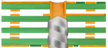
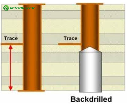
Take the production of a 12-layer PCB as an example. Assume the actual requirement is to achieve electrical connectivity between Layer 1 and Layer 9. In traditional processes, a through-hole is typically drilled through the entire board in one go, followed by plating the hole wall to enhance conductivity. However, this method connects Layer 1 directly to Layer 12, and the plated metal between Layer 10 and Layer 12, which is not involved in the wiring, forms a protruding “metal pillar.” This “metal pillar” is not only useless but also interferes with the signal transmission path, especially in high-speed communication scenarios, where it easily causes signal integrity issues—such as signal delay and noise interference. To solve this problem, engineers perform a secondary drilling operation from the backside of the circuit board to remove this excess “metal pillar” (commonly referred to in the industry as a “stub”). This process is pcb back drilling, performed on plated through holes to remove unwanted conductive layers and via stubs. When configuring back drilling, it is crucial to select the first and last layers involved in the operation to ensure precise removal of the stub. However, due to process limitations, back drilling cannot achieve complete removal without any residue: on one hand, subsequent plating processes will form a small amount of copper layer on the hole wall; on the other hand, the pointed structure of the drill bit itself will also leave a tiny residual tip at the bottom. The length of this residual portion is referred to in the industry as the “B-value,” which is strictly controlled within a range of 50-150 micrometers (μm) to minimize its impact on the signal. Back drilling helps reduce signal reflection and preserve the original signal in high-speed PCB applications.
Core Advantages of Back Drilling TechnologyThe widespread application of back drilling in multi-layer PCB manufacturing stems from its outstanding advantages in performance optimization, cost control, process simplification, and more:
Signal Quality Optimization: Effectively reduces noise interference and deterministic jitter, lowers the bit error rate (BER) during signal transmission, optimizes impedance matching, reduces signal attenuation, maintains stable transmission of high-frequency signals, and significantly enhances overall signal integrity. By minimizing signal noise and crosstalk, back drilling is essential for retaining signal integrity in high-speed designs.
Process and Cost Balance: Compared to buried and blind via processes, back drilling can reduce the use of special via types, lowering the technical difficulty of PCB production. Compared to sequential lamination processes, it is more cost-effective, has minimal impact on circuit board design and layout, and does not require major adjustments to the original design. Adopting proper design and manufacturing practices helps mitigate signal integrity issues and ensures process accuracy.
Performance Potential Enhancement: By removing stubs, it reduces electromagnetic interference/electromagnetic compatibility (EMI/EMC) radiation generated at the stub end, decreases the probability of exciting resonance modes, reduces crosstalk between vias, and thereby increases channel bandwidth and data transmission rates, supporting performance breakthroughs in high-end electronic devices. Back drilling helps reduce signal reflections and increases signal integrity, especially in high-frequency applications.
Strong Structural Adaptability: Enables local thinning of PCB thickness, meeting the differentiated requirements for board thickness in some special equipment, and expands the application scenarios of PCBs in complex products.
Typical Characteristics of Back Drilling TechnologyIn practical applications, back drilling technology has clear scope of application and parameter standards, which determine its suitability for different PCB products:
Applicable Board Types: Mainly used for rigid PCBs. These boards have a stable structure, which better facilitates precise positioning and drilling operations during back drilling. Flexible boards are less likely to use back drilling due to their material properties.
Layer Number Requirement: Typically applicable to multi-layer PCBs with 8 layers or more. PCBs with fewer layers (e.g., 4 or 6 layers) have relatively lower demands for signal integrity, making back drilling optimization unnecessary. For PCBs with more than 8 layers, due to their complex inter-layer structure and long signal transmission paths, the necessity of back drilling significantly increases. Detailed pcb layers data is important for high-speed signal integrity and proper back drilling configuration.
Board Thickness Standard: Board thickness must exceed 2.5 millimeters (mm). In thinner PCBs, the stub length after drilling through-holes is relatively short, having less impact on signals. For PCBs thicker than 2.5mm, the stub length is prone to exceed standards and must be removed via back drilling.
Hole Size Parameters: The minimum via diameter is 0.3 millimeters (mm), and the back drill diameter (the diameter of the drill bit used for back drilling) must be 0.2 mm larger than the via diameter. This size difference ensures the stub is fully removed while avoiding damage to the original plating on the hole wall. The back drill diameter should be slightly larger than the primary drill size to ensure effective stub removal.
Precision Requirements: The tolerance for back drill depth must be controlled within ±0.05 millimeters (mm). This extremely small tolerance range is key to ensuring signal transmission stability. Excessive depth deviation may result in incomplete stub removal or damage to the underlying circuits.
The Complete Production Process of Back DrillingThe pcb manufacturing process must strictly follow sequential steps, as the quality of each operation directly affects the final outcome. The specific process is as follows:
Positioning and Initial Drilling: First, pre-drill positioning holes on the PCB board. The purpose of these holes is to provide a precise reference for subsequent drilling. Using the positioning holes as a reference, initial vias (through-holes) are drilled using professional equipment, ensuring the hole positions exactly match the design drawings. Signal travels through these drilled holes and PCB layers, and can be affected by via stubs if not properly managed.
Plating and Sealing After Initial Drilling: The PCB with initial vias undergoes overall plating to enhance hole wall conductivity and board oxidation resistance. Before plating, dry film must be used to seal the positioning holes. This prevents plating solution from entering the positioning holes, avoiding impacts on subsequent positioning accuracy.
Outer Layer Pattern Formation: Through processes like exposure and development, the outer layer circuit pattern is created on the plated PCB surface, defining the circuit paths and connections in preparation for subsequent pattern plating.
Pattern Plating and Secondary Sealing: Local plating is performed on the outer layer circuit pattern to enhance the conductive performance and wear resistance of the lines. Similar to post-initial-drilling plating, the positioning holes must be sealed again with dry film before pattern plating to ensure their cleanliness and precision.
Back Drilling Processing: The positioning holes used in the initial drilling are reused for precise positioning to avoid deviation in the back drill position due to positioning errors. A drill bit matching the via size is selected to perform secondary drilling (back drilling) on the plated holes requiring stub removal. The drilling depth is strictly controlled to ensure stub removal meets the B-value requirement. This step uses back drills, and the configuration of back drill parameters—including the selection of the top layer, last layer, and bottom layer—is managed in the layer stack manager and properties panel of PCB design software. The process must precisely drill holes to remove excess copper material and via stubs, resulting in a back drilled hole that improves signal integrity. The layer stack and its configuration directly impact back drilling operations.
Cleaning and Finishing: After back drilling is completed, drill chips and dust will remain on the PCB board. If not cleaned, this residue can affect subsequent processes (like soldering and assembly). Therefore, specialized cleaning equipment is used to clean the back-drilled holes and the entire board, removing residual impurities and ensuring the PCB surface and holes are clean and tidy. It is also necessary to remove copper plating from the via stubs to prevent high-frequency signal reflections and resonance.
Two Core Challenges of Back Drilling ProcessDespite its significant advantages, two key difficulties in actual production directly determine the success of the process and require focused:
Depth Control ChallengeThe core of back drilling is “depth control.” Its depth tolerance is mainly influenced by two factors: first, equipment accuracy—the precision of the depth measurement module and execution mechanism of the back drilling equipment directly determines the accuracy of the drilling depth; second, dielectric thickness tolerance—deviations in the actual thickness of each PCB layer’s dielectric material can cause the preset drilling depth to not match the actual requirement. Furthermore, external factors can also interfere with depth precision: for example, changes in resistance encountered by the high-speed rotating drill bit may cause unstable drilling speed; wear on the drill tip angle can alter the drilling trajectory; the tightness of contact between the cover board and the equipment’s measurement unit can affect the accuracy of depth detection; even slight warping of the PCB board due to temperature and humidity changes can lead to drilling depth deviations. Therefore, comprehensive control is needed in production: selecting drill bit materials with high hardness and wear resistance; regularly calibrating the equipment’s measurement module; pre-treating the PCB board for temperature and humidity to reduce warping; and adjusting drilling parameters through test drills to ensure depth accuracy meets standards. Manufacturing practices are essential to ensure process accuracy and signal integrity.
Alignment Accuracy ChallengeBack drilling involves secondary drilling based on the initial holes. The coincidence degree of these two drilling operations (i.e., alignment accuracy) is crucial—excessive alignment deviation can damage the hole wall plating or even accidentally drill through underlying circuits. Factors affecting alignment accuracy mainly fall into three categories: first, board expansion and contraction—PCBs may experience due to temperature changes during processes like plating and baking, causing initial hole positions to shift; second, equipment accuracy—errors in the positioning system of the back drilling equipment directly affect the positional accuracy of the secondary drilling; third, drilling method—different clamping methods and drilling speeds can affect the stability of the PCB board, leading to alignment deviations. To address this, multiple measures must be taken in production: optimize process parameters to reduce board expansion and contraction; regularly maintain the positioning system of the back drilling equipment to ensure positioning errors are within allowable limits; use more stable board clamping devices; and control drilling speed and pressure to ensure precise coincidence between secondary drilling and initial holes.
Main Application Fields of Back Drilling TechnologyAs back drilling can significantly improve the stability of high-frequency signal transmission, its applications are mostly concentrated in fields with extremely high demands for signal quality and equipment reliability:
Communication Equipment: Devices like 5G base stations, routers, and switches need to handle large amounts of high-speed data signals. Back drilling can reduce signal interference and ensure stable communication quality.
Large Servers: Servers require 24/7 uninterrupted operation and handle massive data transmission. Back drilling can reduce signal attenuation and bit error rate, ensuring server efficiency and reliability.
Medical Electronics: Medical imaging equipment (e.g., CT, MRI), patient monitors, etc., have stringent requirements for signal accuracy. Back drilling can prevent signal distortion, ensuring the accuracy of medical data.
Military and Aerospace: Military equipment and spacecraft operate in complex environments (e.g., high temperature, vibration, strong electromagnetic interference). Back drilling can enhance the anti-interference capability and stability of PCBs, meeting usage requirements in extreme environments.
Alternative Solutions and StrategiesIn addition to back drilling, alternative strategies such as microvias, blind and buried vias, and alternative stack up arrangements can be used to minimize via stub length and improve signal integrity. Laser drilled vias are a precise method for creating microvias, especially in high-frequency designs. These alternative stack up arrangements move traces to layers closer to the via ends, reducing the need for back drilling and helping to reduce signal reflection and resonance at high frequencies.
For a visual representation of the back drilling process and its results, refer to the below image.
PCBMASTER, as a professional electronic manufacturing service provider, offers diversified services the entire PCB industry chain, covering PCB prototyping and mass production, SMT assembly, PCB design, electronic module sales, and CNC machining. Whether facing the high-precision needs of the communication and medical fields, or the stringent standards of the military and aerospace sectors, PCBMASTER can, through standardized production processes and personalized technical support, meet the diverse needs of creators and enterprises worldwide in terms of quality control, delivery efficiency, and cost optimization, helping to rapidly turn electronic product design concepts into physical products.
Introduction to Controlled Depth Drilling
Controlled Depth Drilling (CDD), also called back drilling, is a specialized drilling process used in the fabrication of printed circuit boards (PCBs) to enhance signal integrity, especially in high-speed and high-frequency applications. In this process, the drilling is carefully controlled to a specific depth, targeting the removal of the unused portion of the copper barrel within plated through-holes. These unused sections, known as via stubs, can cause signal reflections and degrade signal quality if left unaddressed. By precisely removing these stubs, controlled depth drilling helps maintain signal integrity, reduces signal degradation, and ensures that high-frequency signals travel along the intended path without interference. CDD is a critical step in modern PCB manufacturing, particularly for designs where high-speed data transmission and minimal signal loss are essential.
Principles of Back Drilling Technology
The core principle behind back drilling technology is the removal of excess via stubs or unwanted portions of plated through-holes to improve signal integrity in printed circuit boards. The back drilling process involves re-drilling the existing holes with a slightly larger drill bit, which effectively removes the unwanted copper plating that forms the stub. The selection of drill bit size and the precise control of drill depth are crucial, as they determine how much of the stub is eliminated without damaging the functional part of the via. By minimizing the stub length, back drilling significantly reduces signal reflections and enhances overall signal quality. This process is especially important in high-speed and high-frequency PCB designs, where even small amounts of unwanted copper can lead to data errors and signal degradation. The use of a slightly larger drill bit ensures that only the unnecessary copper is removed, leaving the rest of the via intact and maintaining the integrity of the signal path.
The Back Drilling Process
The back drilling process is a carefully controlled sequence of steps designed to optimize the performance of high-speed circuit boards. It begins with identifying which vias or plated through-holes require back drilling, typically those that extend beyond the necessary signal layer connections. Next, the appropriate drill bit size is selected—usually 8-10 mils larger than the original drill diameter—to ensure that the unwanted copper plating is fully removed. The drilling depth is then calculated based on the specific requirements of the PCB design, ensuring that only the unused portion of the via is eliminated. During the re-drilling, the slightly larger drill bit is used to carefully remove the excess copper without affecting the functional part of the via. After the back drilling process, the holes are often filled with epoxy material to prevent solder wicking and to provide additional mechanical stability. This entire process requires specialized equipment and skilled operators to ensure that the circuit board is back drilled accurately and efficiently, preserving the integrity of the remaining via structure.
Advantages of Back Drilling
Back drilling offers several significant advantages in the manufacturing of high-speed printed circuit boards. By removing excess via stubs or portions of plated through-holes, back drilling greatly improves signal integrity and reduces signal reflections, which are critical for maintaining high signal quality and reliable signal transmission. This process helps to minimize signal degradation and ensures that high-speed signals travel along their intended paths without interference. Compared to more complex and costly techniques such as sequential lamination for blind and buried vias, back drilling is a cost-effective solution that achieves similar improvements in signal performance. It is particularly valuable in high-speed digital designs and RF circuits, where even minor signal integrity issues can lead to data errors or system failures. By optimizing the signal path and reducing unwanted copper, back drilling is an essential technique for producing high-performance PCBs.
Applications of Back Drilling
Back drilling is widely used in the production of high-speed printed circuit boards across a variety of industries where signal integrity is paramount. In telecommunications, back drilling is essential for ensuring the reliable transmission of high-speed signals in equipment such as routers, switches, and 5G base stations. The aerospace and defense sectors rely on back drilling to maintain signal integrity in mission-critical systems that operate in challenging environments. Medical devices, automotive electronics, and industrial control systems also benefit from back drilling, as these applications demand high-speed signal transmission with minimal signal reflections and noise. By improving signal integrity and reducing the risk of signal degradation, back drilling plays a crucial role in the performance and reliability of advanced electronic systems that require the highest standards of signal quality.
FAQs
Q. On which types of PCBs is back drilling generally applied, and what are its characteristics?
A. Back drilling is typically applied to PCBs with 8 or more layers and a board thickness greater than 2.5mm, where the back side is mostly rigid. The minimum keep-out dimension is 0.3mm, the back drill diameter is 0.2mm larger than the via hole, and the back drill depth tolerance is ±0.05mm. PCBs for products such as communication equipment and large servers, which have high requirements for signal integrity, often adopt back drilling technology.
Q. How is the depth of back drilling controlled, and what are the challenges?
A. The depth of back drilling is defined by configuring drill pairs, specifying the start and stop layers of the back drill. The challenges lie in the significant impact of equipment precision and dielectric thickness tolerance. Equipment aging, improper maintenance, or defects in control software may lead to inaccuracies in drilling position and depth. Errors during the design phase, such as incorrect drilling positions or hole size dimensions, as well as process errors, such as improper drilling parameter settings or drill bit wear, can also affect the control of back drilling depth.
Q. What are the requirements for drill bit selection during back drilling?
A. Drill bit selection depends on the drilling diameter, the hardness of the PCB material, and the required drilling speed and precision. Typically, carbide drill bits are widely used due to their excellent durability and cutting performance. The drill bit diameter is generally about 4–6 mils larger than the inner diameter of the via hole (or 0.2mm larger), determined specifically based on the through-hole size and board thickness. Additionally, the coating and geometric shape of the drill bit must be considered, as these factors affect the efficiency of the back drilling process and the quality of the hole wall.
Why PCBMASTER: https://www.pcbmaster.com/why
Join US:https://www.pcbmaster.com/login

