


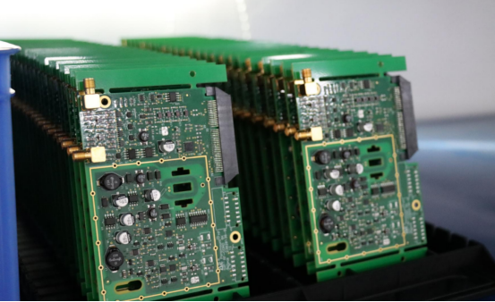
What Is a PCB Assembler and How They Work in Manufacturing
In modern electronics manufacturing, precision and reliability depend heavily on the work of PCB assemblers. But what exactly is a PCB assembler, and how do they contribute to the production process? A PCB assembler is responsible for mounting and soldering electronic components onto a printed circuit board (PCB), transforming a bare board into a fully functional assembly. Their expertise bridges the gap between PCB fabrication and finished electronic products, ensuring that every connection, component, and solder joint meets strict quality standards.
Introduction to PCB Assemblers
Definition of a PCB Assembler
A PCB assembler is a skilled technician or specialized company responsible for placing and soldering electronic components onto a printed circuit board (PCB). This process transforms a bare board—essentially a sheet of insulating material with copper traces—into a fully functional electronic assembly known as a PCBA (Printed Circuit Board Assembly).
In simple terms, a PCB assembler turns design into reality. They follow detailed design files and bills of materials (BOMs) to mount resistors, capacitors, ICs, and connectors on the board with precise accuracy. Depending on the project, this work can be done manually, using soldering tools and microscopes, or automatically, through advanced machinery such as SMT (Surface Mount Technology) pick-and-place systems.
It’s important to distinguish between PCB assembler and PCB assembly:
PCB assembler refers to the individual or company performing the work.
PCB assembly (PCBA) refers to the process and final product that results from mounting and soldering components onto the board.
In addition to SMT, many assemblers also use THT (Through-Hole Technology), where component leads are inserted into drilled holes and soldered to the opposite side of the board. The combination of SMT and THT techniques allows assemblers to handle both compact, high-speed circuits and mechanically strong connections.
Importance of PCB Assemblers in Modern Manufacturing
PCB assemblers play a critical role in the electronics manufacturing value chain. They serve as the bridge between PCB fabrication—where the bare boards are produced—and final product assembly, where the circuit boards are integrated into devices. Without precise assembly, even the best-designed circuits cannot function reliably.
Their work directly affects the functionality, reliability, and scalability of electronic systems. For example:
In consumer electronics, PCB assemblers ensure smartphones, laptops, and wearables operate efficiently under high-density layouts.
In industrial equipment, they assemble durable PCBs capable of withstanding heat, vibration, and continuous use.
In medical devices and LED lighting, they guarantee consistent performance where accuracy and safety are paramount.
Beyond technical execution, assemblers also contribute to production efficiency and innovation. By optimizing assembly processes, selecting the right soldering techniques, and implementing automated inspection systems, they help manufacturers achieve higher yields, lower costs, and faster time-to-market.
In summary, a PCB assembler is the essential link that transforms electronic design into reliable, scalable, and high-performing hardware ready for real-world applications.
The Role and Responsibilities of a PCB Assembler
Core Duties
A PCB assembler is responsible for turning electronic designs into physical, functioning circuit boards. Their core duties revolve around precision, accuracy, and quality control.
One of their primary tasks is reading and interpreting circuit board schematics and assembly drawings. These documents provide exact details on where each component—such as resistors, capacitors, and integrated circuits—must be placed. Assemblers must understand component polarity, pin orientation, and reference designators to avoid errors that could lead to board failure.
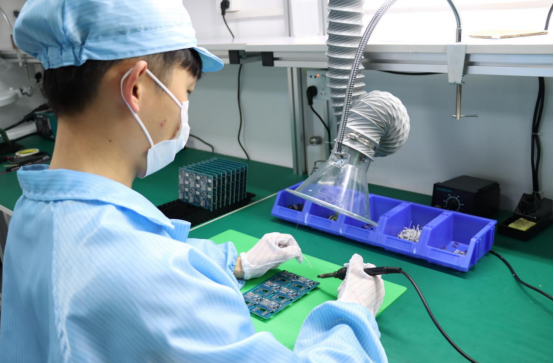
Once the design is understood, the assembler performs component placement and soldering.
In manual assembly, technicians use soldering irons, tweezers, and microscopes to mount components on low-volume or prototype boards.
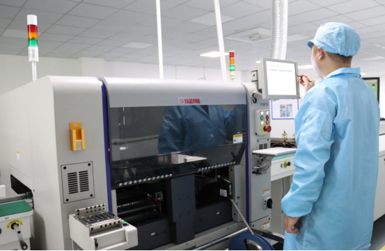
In automated assembly, machines like pick-and-place systems position components at high speed, followed by reflow or wave soldering to secure them permanently.
After assembly, quality control checks are critical. Assemblers use visual inspection, AOI (Automated Optical Inspection), and sometimes X-ray testing to ensure every solder joint is solid and each component is correctly aligned. These checks prevent defects such as solder bridges, missing parts, or reversed components before boards move to final testing.
Technical Skills and Tools Used
PCB assemblers combine hands-on craftsmanship with technical expertise. Their work requires familiarity with both assembly equipment and industry standards.
Common tools used by PCB assemblers include:
Pick-and-place machines: Automatically place surface-mount components on PCBs with micron-level precision.
Soldering stations and reflow ovens: Heat solder paste to create reliable electrical connections.
AOI (Automated Optical Inspection) systems: Detect misplacements, solder defects, or missing parts.
ESD-safe workstations: Prevent electrostatic discharge that can damage sensitive components.
Essential skills for PCB assemblers include:
Manual and automated soldering techniques for both SMT (Surface Mount Technology) and THT (Through-Hole Technology).
Component identification and orientation to ensure each part is placed correctly.
Understanding of IPC-A-610 standards, the global benchmark for electronic assembly quality.
Attention to ESD (Electrostatic Discharge) safety, ensuring product reliability.
These technical abilities allow assemblers to maintain consistent product quality while adapting to different board types and production volumes.
Collaboration with Design and Manufacturing Teams
PCB assemblers do not work in isolation—they are part of a collaborative production ecosystem. They regularly coordinate with PCB designers, engineers, and production managers to ensure that every board can be built efficiently and cost-effectively.
One key area of collaboration is Design for Manufacturability (DFM). Assemblers provide feedback on board layout, component spacing, and solder joint accessibility. This DFM feedback loop helps designers adjust their layouts before production, reducing rework, waste, and assembly time.
For example, an assembler might notice that components are too close for a soldering nozzle or inspection camera. By flagging this early, the design team can make spacing adjustments before mass production begins. This partnership between design and assembly teams ensures a smoother workflow, higher yields, and faster time-to-market.
How PCB Assemblers Work — Step-by-Step Process
The work of a PCB assembler follows a structured, repeatable process designed to ensure precision, reliability, and consistency in every circuit board. From material preparation to final packaging, each step plays a vital role in turning a bare PCB into a fully functional electronic assembly.
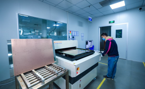
Step 1 – Material Preparation
Every successful assembly begins with accurate material preparation. PCB assemblers first collect all necessary materials, including bare circuit boards, electronic components, solder paste, and metal stencils used for printing.
Before assembly begins, they review the Bill of Materials (BOM) — a detailed list that specifies every part, component value, and placement location.
Assemblers begin by verifying that all materials match the design files and are free from defects. Components are then organized by type and size to streamline the placement process, ensuring efficiency and accuracy during assembly. Additionally, environmental controls—such as humidity and temperature—are carefully monitored to maintain component stability and prevent damage throughout the production process.
In short, material preparation ensures the right components are in the right place before production begins.
Step 2 – Solder Paste Application
The next step is applying solder paste to the PCB’s pads, where electronic components will later be mounted. This is done using a stencil printing process:
1. A stainless-steel stencil—custom-cut to match the pad layout—is placed over the PCB.
2. Solder paste, a mixture of tiny solder particles and flux, is spread across the stencil.
3. A squeegee blade moves over the stencil, filling each opening with paste.
Once the stencil is lifted, a precise layer of solder paste remains on each pad. Assemblers then inspect the printed paste to ensure uniform thickness and clean edges, since poor paste application can cause bridging or open circuits later.
Common quality checks include microscopic inspection and automated paste inspection systems (SPI) to verify print accuracy.
Step 3 – Component Placement
After the solder paste is applied, components are positioned onto the PCB in their designated locations.
There are two main types of placement:
Manual placement: Used for prototypes or low-volume runs. Technicians place components by hand using tweezers and visual aids.
Automated placement: For large-scale production, assemblers use pick-and-place machines that rapidly position thousands of components per hour.
Example: A high-speed pick-and-place system can align tiny 0201-sized resistors (only 0.6 × 0.3 mm) onto precise pads with optical cameras ensuring micron-level accuracy.
After all components are placed, the board is ready for soldering.
Step 4 – Soldering Process
The soldering process permanently attaches the components to the PCB. Different soldering methods are used depending on the assembly type:
Reflow soldering (for SMT components):
The assembled board passes through a reflow oven, where it is gradually heated to melt the solder paste and form reliable electrical connections; during this process, the temperature follows a controlled profile of preheat, soak, reflow, and cooling stages, while automated systems ensure even heating to prevent damage to sensitive components and guarantee consistent solder joint quality.
Wave soldering (for THT components):
Through-hole boards are passed over a wave of molten solder, which coats and connects all component leads simultaneously. Assemblers often perform inspection during and after soldering, checking for cold joints, bridging, or insufficient solder.
Step 5 – Inspection and Testing
Once soldering is complete, the PCB undergoes a series of inspection and testing procedures to confirm quality and performance.
Common methods include:
AOI (Automated Optical Inspection): Uses cameras to detect missing, misaligned, or incorrectly oriented components.
X-ray inspection: Used for hidden joints (like BGA packages) where visual checks are impossible.
Functional testing: Applies power to the board and verifies that circuits operate correctly.
Early detection of defects—such as solder bridges, shorts, or reversed components—saves time and prevents costly rework later.
Effective inspection ensures every board meets quality standards before reaching the next production stage.
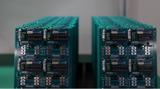
Step 6 – Final Assembly and Packaging
After testing, the PCBs move to final assembly and packaging.
After soldering, boards are carefully cleaned to remove flux residues and any contaminants that could compromise performance. In some cases, a conformal coating is applied, providing a thin protective layer that shields the circuits from moisture, dust, and corrosion. Finally, the boards are labeled, serialized, and packaged for shipment, with traceability labels ensuring that each board can be tracked back to its specific production batch and material lot.
Packaging often includes anti-static bags, foam inserts, and humidity-control pouches to protect sensitive electronics during transportation.
Types of PCB Assemblers
PCB assembly can be carried out in different ways depending on production volume, complexity, and precision requirements. Broadly, PCB assemblers are categorized into manual, automated, and hybrid types, each with distinct capabilities and applications.
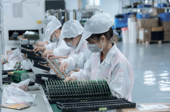
Manual PCB Assemblers
Manual PCB assemblers are human technicians who place and solder components on low-volume or prototype boards. They are highly skilled at handling small or delicate components and can adapt to changes quickly during the assembly process.
Use case example: Startups or R&D labs often rely on manual assemblers to produce prototypes because human technicians can make rapid adjustments without reprogramming machinery.
Advantages: Flexibility, quick turnaround, ability to handle complex or irregular components.
Limitations: Slower production speed and higher labor costs compared to automation.
In essence, manual assembly is ideal for projects where quality and adaptability matter more than volume.
Automated PCB Assemblers
Automated PCB assemblers use robotic systems and SMT (Surface Mount Technology) machines to assemble boards at high speed. These systems are designed for large-scale production and can place thousands of components per hour with high precision.
Use case example: Consumer electronics manufacturers, such as smartphone or laptop producers, rely on automated assemblers to produce boards consistently and efficiently at scale.
Advantages: High throughput, precise placement, consistent quality, and reduced human error.
Limitations: High initial investment in machinery, less flexibility for design changes during production.
Automation excels in repetitive, high-volume production where speed and uniformity are critical.
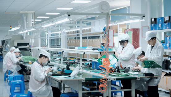
Hybrid PCB Assemblers
Hybrid PCB assemblers combine human skill and automated machinery to handle boards with mixed technologies, high component density, or precision requirements that are difficult for machines alone.
Use case example: Complex medical devices or aerospace electronics where some components require manual soldering while others are placed automatically.
Advantages: Balances speed and precision, allows for complex designs, reduces human fatigue while retaining adaptability.
When used: High-density boards, multi-layer designs, or small production runs with sophisticated components.
Hybrid assembly provides the best of both worlds: automation for efficiency and humans for flexibility and quality assurance.
Differences Between PCB Assembler and PCB Manufacturer
Understanding the distinction between a PCB manufacturer and a PCB assembler is essential for anyone involved in electronics production. While both roles are critical to the lifecycle of a printed circuit board, they focus on different stages and processes.
PCB Manufacturer
A PCB manufacturer is responsible for fabricating the bare circuit board. This process involves multiple steps:
Etching copper layers: Removing excess copper from the board to form precise circuit traces.
Laminating layers: Combining multiple layers of dielectric material and copper to form multi-layer PCBs.
Drilling and plating: Creating vias and through-holes for electrical connections.
The output of a PCB manufacturer is a bare PCB, which has no electronic components but is ready to be assembled.
Example: A company that produces single-layer or multi-layer boards for smartphones or industrial sensors is a PCB manufacturer.
PCB Assembler
A PCB assembler, in contrast, is responsible for populating the bare board with electronic components to create a fully functional assembly (PCBA).
Components such as resistors, capacitors, ICs, and connectors are mounted onto the PCB using either manual or automated techniques. Following placement, soldering, inspection, and testing are performed to ensure that each board functions correctly. Through this process, the assembler transforms a bare board from the PCB manufacturer into a finished, fully functional circuit board, ready for integration into electronic devices.
Example: A factory using pick-and-place machines and reflow ovens to assemble motherboards for laptops is acting as a PCB assembler.
Comparison Table
Aspect PCB Manufacturer PCB Assembler Focus Bare board fabrication Component assembly Key Equipment Drilling, etching, plating machines Pick-and-place machines, reflow ovens, AOI systems Output Bare PCB Fully functional PCBA Expertise
Material science, board design, fabrication processes
Soldering, component placement, quality control
Primary Goal
Produce reliable and precise circuit boards
Turn bare boards into working electronics
| Aspect | PCB Manufacturer | PCB Assembler |
|---|---|---|
| Focus | Bare board fabrication | Component assembly |
| Key Equipment | Drilling, etching, plating machines | Pick-and-place machines, reflow ovens, AOI systems |
| Output | Bare PCB | Fully functional PCBA |
Expertise | Material science, board design, fabrication processes | Soldering, component placement, quality control |
Primary Goal | Produce reliable and precise circuit boards | Turn bare boards into working electronics |
This comparison clarifies that while PCB manufacturers create the canvas, PCB assemblers bring the circuit to life. Both roles are interdependent and essential for producing high-quality electronic devices.
Quality Standards and Certifications in PCB Assembly
Maintaining high-quality PCB assembly is essential to ensure reliable and long-lasting electronic products. PCB assemblers follow recognized standards, rigorous testing, and consistent process controls to guarantee product integrity.
Common Industry Standards
PCB assemblers adhere to several industry standards to ensure the safety, reliability, and regulatory compliance of electronic assemblies:
IPC-A-610: The globally recognized standard for the acceptability of electronic assemblies. It defines criteria for soldering quality, component placement, and board workmanship.
ISO 9001: A quality management system standard that ensures consistent production processes and continuous improvement.
RoHS Compliance: Restricts the use of hazardous substances in electronics, such as lead and mercury.
UL Certification: Verifies that assemblies meet safety and performance requirements for electrical products.
Example: A PCB assembler producing consumer electronics must meet IPC-A-610 for soldering quality while ensuring all components comply with RoHS environmental standards.
Testing and Quality Control Procedures
PCB assemblers use multiple testing and inspection methods to verify assembly accuracy and prevent defects:
In-Circuit Testing (ICT): Checks electrical performance at the component level by measuring voltage, current, and continuity.
Functional Testing: Verifies that the entire board operates as intended in real-world conditions.
Visual Inspection: Detects misaligned components, solder bridges, or other visible defects.
Maintaining high yield rates is critical, as defective boards can increase costs, delay production, and damage brand reputation. Systematic testing reduces errors and ensures only reliable assemblies move forward.
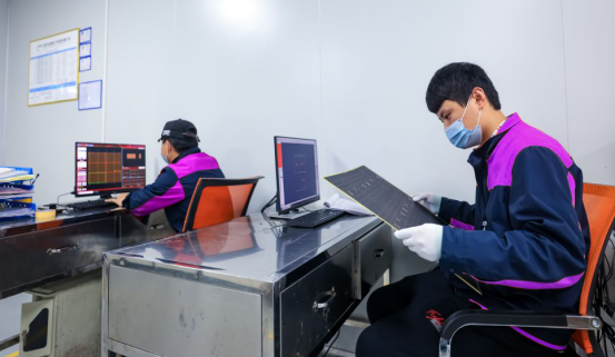
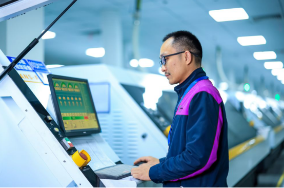
How PCB Assemblers Ensure Consistency
Consistency in PCB assembly is achieved through process control, traceability, and skilled operators:
Traceability Systems: Track each board back to its production batch and component lot, facilitating root-cause analysis in case of defects.
Process Control Software: Monitors placement accuracy, soldering temperatures, and assembly timelines to maintain uniform quality.
Operator Training: Ensures technicians follow best practices for soldering, component handling, and inspection.
Example: An assembler may use automated software to log each pick-and-place action, ensuring every board is assembled according to the same precise standard.
Choosing a Reliable PCB Assembler
Selecting the right PCB assembler is essential for achieving high-quality assemblies, maintaining production efficiency, and meeting project timelines. Manufacturers should carefully evaluate potential partners based on capabilities, certifications, and experience.
Key Factors to Consider
When choosing a PCB assembly partner, focus on several key factors:
Technical Capability: The assembler should handle your required technology, such as SMT, THT, or hybrid assemblies, and be experienced with high-density or complex boards.
Certifications and Compliance: Look for adherence to IPC-A-610, ISO 9001, RoHS, and UL standards to ensure quality and regulatory compliance.
Lead Time: Assess whether the assembler can meet both prototype and mass production schedules.
Communication Quality: Clear, responsive communication ensures design questions, production updates, and issue resolution are handled efficiently.
Example: For a project with high-density micro-BGA components, a partner with proven experience in HDI and SMT assembly will reduce errors and improve efficiency.
Prototype vs. Mass Production Assemblers
PCB assemblers vary based on production volume and flexibility needs:
Prototype Assemblers: These assemblies are ideal for low-volume runs and rapid development cycles, as they offer the flexibility to implement design changes quickly. However, they typically come with a higher per-unit cost due to the reliance on manual labor or the complexity of setup.
Mass Production Assemblers: Automated assembly lines are used for consistent, high-volume production, delivering lower per-unit costs and reliable quality. However, they are less flexible when it comes to accommodating frequent design changes once production is underway.
Comparison: A startup building a prototype sensor may choose manual assembly for adaptability, while a consumer electronics company producing thousands of units would rely on automated mass production.
Example: Evaluating PCB Assembly Partners
To choose a reliable PCB assembler, consider a structured evaluation checklist or scoring system:
Technical Expertise: Ability to handle your board complexity (score 1–5).
Certifications: IPC, ISO, RoHS, and UL compliance (score 1–5).
Equipment & Capacity: Availability of pick-and-place machines, reflow ovens, and AOI systems (score 1–5).
Lead Time: Ability to meet prototypes and production deadlines (score 1–5).
Communication & Support: Responsiveness and guidance during design and production (score 1–5).
Example: PCBMASTER, a seasoned PCB supplier, has a team of skilled PCB assemblers and advanced equipment. They consistently ensure high-quality assemblies, efficient production, and smooth communication, making them an ideal choice for both prototypes and mass production.
Future Trends in PCB Assembly
Automation and Smart Manufacturing
Automation in PCB assembly is evolving beyond traditional pick-and-place and reflow systems. AI, machine vision, and data analytics are increasingly integrated into modern assembly lines to improve accuracy, reduce defects, and optimize production speed. For example, AI-driven visual inspection systems can detect misaligned components or soldering defects faster than human operators, allowing real-time adjustments.
Step-by-step impact of smart manufacturing:
1. Sensors collect real-time data on placement accuracy, solder temperature, and humidity.
2. AI analyzes the data to identify patterns or predict potential defects.
3. Machines adjust processes automatically, such as reflow oven profiles or component placement speeds.
The result is higher yield, faster turnaround, and consistent quality, especially for high-volume or complex PCBs. This trend highlights the shift toward data-driven assembly lines where predictive maintenance and adaptive control reduce downtime and waste.
Miniaturization and Advanced Packaging
Modern electronics demand smaller components, higher density boards, and HDI (High-Density Interconnect) technology, which challenge traditional assembly methods. Components like 0201 resistors, micro-BGAs, and CSPs require ultra-precise placement and specialized soldering techniques.
Challenges and solutions:
Challenge: Reduced pad sizes increase the risk of misalignment or solder bridging.
Solution: High-precision pick-and-place machines with advanced vision systems ensure accurate placement.
Challenge: Multi-layer HDI boards complicate thermal management and via alignment.
Solution: Thermal simulation and controlled reflow profiles prevent hotspots and solder defects.
As electronics shrink and functionality increases, PCB assembly must evolve to handle compact layouts while maintaining reliability. This trend drives investment in micro-component handling, laser soldering, and automated inspection tools.
Sustainability and Green Manufacturing
Sustainability is becoming a key focus in PCB assembly, with companies adopting lead-free solder, energy-efficient equipment, and waste reduction strategies. Lead-free solder, mandated by regulations like RoHS, reduces environmental hazards but requires precise thermal profiles to ensure reliable joints.
Other green initiatives include:
Minimizing scrap: Optimizing stencil design and pick-and-place programming reduces component waste.
Energy efficiency: Smart ovens and conveyor systems lower electricity consumption.
Recycling and material recovery: Collecting solder residues, boards, and unused components for reuse or safe disposal.
By integrating sustainable practices, manufacturers can reduce environmental impact, comply with regulations, and support corporate responsibility goals while maintaining high-quality PCB assembly.
Conclusion
A PCB assembler is a skilled professional or company responsible for mounting and soldering components onto a bare printed circuit board (PCB), transforming it into a fully functional electronic assembly (PCBA). From material preparation and solder paste application to component placement, soldering, inspection, and final packaging, assemblers follow a precise workflow to ensure every board meets strict quality standards.
PCB assemblers play a vital role in turning circuit designs into working products, bridging the gap between PCB fabrication and finished devices. Their expertise ensures functionality, reliability, and scalability across a wide range of electronic applications, from prototypes to high-volume production.
Choosing a reliable PCB assembly partner is crucial for consistent quality and efficient production. Companies like PCBMASTER offer experienced assemblers, advanced equipment, and rigorous process controls, helping manufacturers deliver high-quality PCBs on time and within budget.
FAQs
What qualifications or certifications are required to become a PCB assembler?
To become a PCB assembler, candidates generally need a high school diploma or vocational training in electronics, electrical engineering, or related fields. Some roles prefer an associate degree in electronics technology. Key certifications include IPC-A-610, which defines the acceptability of electronic assemblies, and IPC J-STD-001, focused on soldering processes and materials. Electrostatic discharge (ESD) training is also essential to protect sensitive components. Additionally, PCB assemblers must have practical skills such as soldering, component recognition, and reading schematics to ensure correct assembly.
What is the difference between SMT and THT in PCB assembly?
Surface Mount Technology (SMT) involves placing components directly onto the surface of a PCB. It is suitable for small, high-density boards and works efficiently with automated assembly lines, using reflow soldering to secure components. Through-Hole Technology (THT) requires component leads to go through drilled holes and be soldered on the opposite side, providing stronger mechanical connections. THT is often used for connectors or heavy components and typically employs wave soldering. For example, a microcontroller is usually SMT-mounted, while a sturdy connector might use THT for durability.
How long does a typical PCB assembly process take?
The time required depends on board complexity and production volume. Prototypes may take one to three days, particularly if assembled manually. Low- to mid-volume production usually requires three to seven days, including solder paste application, component placement, soldering, and inspection. High-volume automated production can take several days to a few weeks, but automation accelerates placement and soldering. Factors such as component density, SMT/THT mix, and quality control procedures influence the overall timeline.
What are common challenges in PCB assembly?
Common challenges include misaligned or incorrectly oriented components, soldering defects such as cold joints or solder bridges, and ESD damage to sensitive parts. High-density boards may be difficult to inspect or assemble, and variations in component quality or errors in soldering processes can also create issues. Skilled operators and thorough inspection procedures are critical to overcoming these challenges and ensuring reliable assemblies.
How do PCB assemblers ensure product reliability and quality control?
PCB assemblers maintain high reliability through compliance with standards like IPC-A-610, IPC J-STD-001, and ISO 9001. They use Automated Optical Inspection (AOI) to check component placement, X-ray inspection for hidden joints, and functional testing to verify board operation. Process controls monitor soldering temperatures, placement accuracy, and workflow, while traceability systems track components and production batches to quickly identify and correct defects. Operator training in ESD safety and best practices ensures consistent quality and low defect rates.


