


Unraveling the Magic of PCB Any - Layer Interconnection
In the ever - evolving world of electronics, Printed Circuit Boards (PCBs) are the unsung heroes that hold everything together. As technology marches forward, the demand for smaller, faster, and more efficient electronic devices has led to some incredible innovations in PCB design. Advancements in printed circuit board technology have enabled innovations like Any-Layer Interconnection, making it possible to create denser and more complex circuit boards for modern electronics. One such innovation that has been making waves is the Any - Layer Interconnection technology. So, what exactly is it, and why is it so important? Let’s dive in and find out!
What is PCB Any - Layer Interconnection?
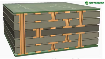
PCB Any - Layer Interconnection, also known as Every Layer Interconnect (ELIC), is a revolutionary approach to PCB design that allows for connections to be made between any two layers of a PCB. In traditional PCB designs, vias (the tiny holes that connect different layers) were limited in their connectivity. They often had to follow a more structured path, and creating connections between non - adjacent layers could be a complex and sometimes limiting process.
With Any - Layer Interconnection, this all changes. The concept is relatively straightforward, yet its implementation is a feat of engineering. Microvias, which are extremely small vias, are used to extend throughout the entire PCB stackup. These microvias are laser - drilled and filled with copper, creating a conductive pathway. Each layer of the PCB has its own set of these copper - filled microvias. Once the layers are stacked, these microvias enable direct connections between any two layers in the board. Advanced designs often use blind vias to enable high-density interconnections, improving electrical performance and space optimization. This means that signals can be routed in a much more flexible and efficient manner, breaking free from the constraints of traditional via - based connectivity.
Any-Layer Interconnection is widely used in advanced layer PCB designs, such as HDI PCBs, to achieve high density interconnect structures. HDI boards leverage these technologies, including microvias and blind vias, to create more compact and efficient circuit layouts, supporting the miniaturization and high performance required in modern electronic devices.
How Does it Work?

The production process of a PCB with Any-Layer Interconnection is a multi-step process that requires precision and advanced technology, involving multiple precise steps to ensure quality and reliability.
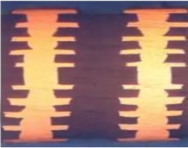
Step 1: Starting with a Base LayerThe process begins with an ultra-thin core layer. Laser-drilling technology is used to create microvias in this base layer. These microvias are then filled with solid copper, forming a solid base for the subsequent layers. The use of filled vias is crucial for structural integrity and reliable electrical performance.
Step 2: Adding Dielectric Layers and More MicroviasAfter the initial microvias in the inner layer are filled with copper, a dielectric layer (a non-conductive material) is added on top through a process called sequential lamination. Once the new layer is in place, laser drilling is once again applied to create microvias in this new layer. The dimensions of the drilled holes and their aspect ratio are critical for ensuring reliable copper plating and overall via integrity. These microvias are then filled with copper as well.
Step 3: Repeating the ProcessThis process of adding a dielectric layer, laser-drilling microvias, and filling them with copper is repeated layer by layer until the desired number of layers and the final PCB stackup is achieved. The end result is a PCB with multiple layers of stacked, copper-filled in-pad microvias that enable complex interconnections between any two layers. A smaller aspect ratio in microvias improves reliability and allows for narrower trace widths, which are essential for high-density designs.
PCB Design and Stack-Up
The foundation of Any-Layer HDI PCBs lies in thoughtful PCB design and meticulous stack-up planning. The stack-up refers to how multiple layers are arranged within a circuit board, and this arrangement is crucial for achieving the high density and reliable interconnects that modern electronic devices demand. In Any-Layer HDI PCBs, designers can connect any two layers directly, thanks to the strategic use of blind and buried vias. These specialized vias allow for connections between different layers without traversing the entire board thickness, freeing up valuable space and enabling more compact circuit layouts.
A well-designed stack-up not only maximizes the use of available space but also plays a pivotal role in maintaining signal integrity and electrical performance. By carefully selecting the order and composition of each layer, designers can minimize signal loss, reduce power consumption, and manage heat dissipation more effectively. This is especially important in high-speed and high-density applications, where even minor design missteps can lead to signal degradation or increased power draw. Ultimately, the stack-up in Any-Layer HDI PCBs is tailored to the actual needs of the device, ensuring that every layer contributes to the overall performance and reliability of the circuit board.
Manufacturing Process
Creating Any-Layer HDI PCBs is a sophisticated process that combines advanced technology with precision engineering. It all starts with the construction of individual layers, each carefully fabricated to meet the specific requirements of the final circuit board. These layers are then stacked and laminated together, forming the backbone of the board’s structure.
One of the defining steps in this process is laser drilling, which is used to create ultra-fine microvias that connect the different layers. These microvias are then filled with copper, establishing robust electrical pathways that enhance signal integrity and reduce signal reflection. The plating process follows, where a thin layer of copper is deposited across the board’s surface, further improving conductivity and ensuring reliable interconnections throughout the entire board.
Every stage of the manufacturing process, from layer construction to laser drilling and plating, requires specialized equipment and a high level of expertise. This meticulous approach ensures that the finished HDI PCBs meet the stringent demands of modern electronics, delivering high performance, reliability, and the ability to support complex circuit layouts in a compact form factor.
The Advantages of Any-Layer Interconnection
Any-Layer interconnection technology brings a host of advantages to PCB design, setting a new standard for performance and efficiency. One of the standout benefits is the significant improvement in signal integrity. By allowing direct connections between any two layers, designers can optimize signal paths, minimize interference, and maintain high signal quality even in densely packed boards.
Another key advantage is the ability to achieve higher wiring density without increasing the size of the circuit board. This means more functionality can be packed into less space, which is essential for today’s compact electronic devices. Additionally, Any-Layer interconnection helps reduce overall power consumption by shortening signal paths and minimizing resistance, contributing to longer battery life and more energy-efficient products.
By addressing common challenges in PCB design—such as signal integrity issues, limited routing options, and high power consumption—Any-Layer interconnection empowers engineers to create innovative, high-performance electronic equipment that meets the demands of the modern world.
The Advantages of Any - Layer Interconnection
Enhanced Design Flexibility
Any - Layer Interconnection gives PCB designers a level of freedom that was previously unheard of. They can now route signals in ways that were impossible with traditional PCB designs. This is especially useful when dealing with complex circuits that require a large number of connections. For example, in high - speed applications where minimizing signal interference is crucial, designers can use Any - Layer Interconnection to route signals in a way that reduces cross - talk and ensures optimal signal integrity.
Increased Interconnect Density
As electronic devices continue to shrink in size, the need for higher-density interconnects becomes more pressing. Layer PCBs with advanced layer technology allow for more connections in less space, supporting complex, high-performance applications. In some designs, only one layer may be used for specific functions, while others use multiple layers for higher density and versatility. Any-Layer Interconnection allows for a significant increase in the density of interconnects on a PCB, and can help achieve the same functionality with fewer layers, reducing cost and complexity. By enabling connections between any two layers, designers can fit more components and connections into a smaller space. This is essential for applications such as smartphones, wearables, and other portable devices where space is at a premium.
Elimination of Through-Hole Vias
One of the most transformative aspects of Any-Layer HDI PCBs is the reduction or complete elimination of traditional through-hole vias. In conventional circuit boards, through-hole vias can introduce signal reflections and electromagnetic interference, which can compromise signal integrity and overall board performance. By leveraging blind and buried vias, Any-Layer HDI PCBs connect different layers without the need for holes that pass through the entire board.
This approach not only improves signal quality but also allows for more efficient use of board space, enabling higher component density and more complex circuit layouts. The reduction of through-hole vias is particularly beneficial in high-speed applications found in consumer electronics and industrial automation, where maintaining clean, interference-free signals is critical. As a result, Any-Layer HDI PCBs are the go-to solution for designers seeking to push the boundaries of performance and miniaturization in their products.
Elimination of Through - Hole Vias
In traditional PCB designs, through - hole vias were often used to connect different layers. However, with Any - Layer Interconnection, through - hole vias are no longer necessary. Stacked vias are used in Any-Layer Interconnection to create a reliable interconnect solution for complex, high-density designs, enabling higher interconnectivity and improved electrical performance. Since all connections within the PCB are created during the initial buildup using the copper - filled microvias, there is no need for the larger and more space - consuming through - hole vias. This not only saves space but also simplifies the manufacturing process in some ways.
Improved Electrical Performance
The use of copper-filled microvias in Any-Layer Interconnection PCBs results in better electrical conductivity compared to some traditional via-based designs. The use of fine copper traces in these designs contributes to higher wiring density and improved signal quality. This leads to lower resistance and inductance, which in turn improves the overall electrical performance of the PCB. Any-Layer Interconnection is often chosen for applications requiring high reliability, such as aerospace and automotive electronics. The technology also supports the integration of high power components by improving thermal management and electrical performance. In high-speed applications, this can translate into faster signal transmission and reduced signal loss.
Circuit Board Materials
The choice of materials in Any-Layer HDI PCBs is a key factor in achieving high density, reliability, and superior signal integrity. The substrate, often made from advanced materials like FR4 or polyimide, provides a stable and durable foundation for the circuit board, capable of withstanding the mechanical and thermal stresses of both manufacturing and operation. For the conductive layers, high-quality copper foil is used, ensuring excellent electrical performance and the ability to handle the fine features required by HDI technology.
Advanced manufacturing techniques, such as laser drilling and state-of-the-art plating technology, are employed to create precise microvias and robust copper interconnections. These processes not only enhance the electrical performance of the board but also contribute to its long-term reliability, even in demanding environments.
Material selection is tailored to the specific needs of the application—whether it’s the compactness required for mobile devices, the stringent reliability standards of medical devices, or the ruggedness needed for industrial settings. By carefully balancing factors like thermal management, power consumption, and signal integrity, manufacturers ensure that Any-Layer HDI PCBs deliver optimal performance across a wide range of high-density, high-performance electronic devices.
Applications of Any - Layer Interconnection PCBs
Consumer Electronics
Any - Layer Interconnection PCBs are finding their way into a wide range of consumer electronics. In smartphones, for example, they are used to enable the complex integration of various components such as the processor, memory, and wireless communication modules. The increased design flexibility and interconnect density allow manufacturers to pack more functionality into a smaller space, leading to slimmer and more powerful smartphones.
The integration of smart sensors in consumer electronics is also facilitated by the design flexibility of Any-Layer Interconnection PCBs, enabling advanced features such as real-time data collection and enhanced device performance.
Laptops and tablets also benefit from this technology. The ability to route signals more efficiently helps in reducing heat generation and improving battery life. Additionally, the smaller form factor made possible by Any - Layer Interconnection allows for more compact and lightweight designs.
Gaming Consoles
Gaming consoles are another area where Any - Layer Interconnection PCBs are making a difference. These devices require high - speed data transfer between components such as the graphics processing unit (GPU), central processing unit (CPU), and memory. High density interconnect technology is essential for meeting the performance demands of modern gaming consoles. Any - Layer Interconnection enables the creation of a more efficient and reliable data pathway, resulting in smoother gameplay, better graphics, and faster loading times.
Cameras
In digital cameras, especially high-end DSLRs and mirrorless cameras, there is a need for a large number of connections to handle the complex processing of image data. Any-Layer Interconnection PCBs allow for the integration of components such as image sensors, processors, and storage interfaces in a more compact and efficient manner. This can lead to smaller, lighter cameras without sacrificing performance.
Advances in PCB technology, such as laser-drilled, copper-filled microvias, have enabled the miniaturization and integration of high-performance components in modern cameras, supporting greater reliability and high-speed performance.
High - Speed and High - Density Applications
Any - Layer Interconnection is also well - suited for high - speed applications that demand a high input/output (I/O) density. For example, in Field - Programmable Gate Arrays (FPGAs) where multiple interfaces are being instantiated in the device, this technology allows for the efficient routing of signals. Unlike traditional PCBs, which often rely on mechanical drilling and face limitations in supporting high-density and high-speed requirements, Any-Layer Interconnection enables more complex and compact circuit layouts ideal for these advanced applications.
Some boards that need to support RF routing on PTFE materials may also employ Any - Layer Interconnection. Since routes can sometimes be brief in these applications, the improved electrical performance offered by Any - Layer Interconnection helps in reducing return loss and impedance mismatch.
Challenges and Considerations

Manufacturing Complexity
While Any - Layer Interconnection offers many advantages, it also poses significant challenges in the manufacturing process. The precise laser - drilling and copper - filling processes required to create the microvias demand high - end equipment and skilled technicians. Additionally, not all PCB fabricators have the capabilities to produce Any - Layer Interconnection PCBs with a high yield and without latent reflow faults.
Cost
The cost of manufacturing Any - Layer Interconnection PCBs is generally higher compared to traditional PCB designs. This is due to the need for specialized equipment, more complex manufacturing processes, and the use of high - quality materials. However, as the technology becomes more widespread and manufacturing processes become more efficient, the cost is expected to come down.
Compliance with Standards
According to IPC standards, the stacked microvias in Any - Layer Interconnection PCBs should not span across the entire PCB stackup as it can compromise the reliability of the microvias. Manufacturers need to ensure that their designs and manufacturing processes comply with these standards to guarantee the long - term reliability and performance of the PCBs.
Conclusion
PCB Any - Layer Interconnection is a game - changing technology that is revolutionizing the world of PCB design. It offers enhanced design flexibility, increased interconnect density, improved electrical performance, and has a wide range of applications in various industries. While there are challenges such as manufacturing complexity and cost, the benefits it brings are too significant to ignore. As technology continues to advance, we can expect to see even more widespread adoption of Any - Layer Interconnection in the future, leading to smaller, faster, and more efficient electronic devices. Whether it's in our smartphones, gaming consoles, or high - tech cameras, this technology is quietly powering the next generation of electronics.
FAQs
Q. What is PCB Any-Layer Interconnection?
A. PCB Any-Layer Interconnection, often referred to as "Every Layer Interconnect" or "ELIC (Every Layer Interconnect)," is an advanced design technology that overcomes the limitations of traditional interlayer connections in PCBs. It uses laser drilling to create tiny "microvias" and fills them with copper, enabling direct electrical connections between any two layers of the PCB—unlike traditional PCBs that rely on "connections only between adjacent layers" or "through-holes that span the entire board," allowing for more flexible signal routing.
Q. What are the special requirements for "microvias" in Any-Layer Interconnection?
A. The microvias used in Any-Layer Interconnection are "laser microvias" that typically must meet two core requirements:
Small size: The aperture is generally below 0.15mm (commonly 0.05–0.1mm), significantly smaller than traditional mechanically drilled through-holes (typically ≥0.3mm);
Copper filling: The microvias must be completely filled with copper (not just plated on the walls) to ensure stable electrical performance and avoid interference from "parasitic inductance/capacitance" during signal transmission.
Q. Is the delivery time for Any-Layer Interconnection PCBs longer than that of traditional PCBs?
A. Yes, typically by 1–2 weeks. Traditional PCBs (4 layers) have a delivery time of approximately 5–7 days, while 4-layer Any-Layer Interconnection PCBs require 7–10 days; 8-layer Any-Layer Interconnection PCBs require 12–15 days (traditional 8-layer PCBs take about 8–10 days).
Main time-consuming factors: "Layer-by-layer alignment + inspection" during multilayer stacking, and the "curing + planarization" process after microvia filling (to ensure a flat surface that does not affect subsequent component soldering).
Q. What special requirements need to be communicated to engineers when designing Any-Layer Interconnection PCBs?
A. Three key pieces of information must be clarified in advance:
Signal priority: Identify which signals are "high-speed signals" (e.g., 5G, USB4) and need priority planning for the "shortest path" to avoid detours;
Current requirements: Specify the maximum current for each microvia (recommended not to exceed 3A) to prevent overheating due to current overload;
Inspection requirements: Request that the manufacturer provide a "microvia filling inspection report" (e.g., X-ray images) and a "layer alignment inspection report" to ensure process compliance.
Why choose PCBMASTER: https://www.pcbmaster.com/why
Join us: https://www.pcbmaster.com/login

