


The Overlooked Electronic Cornerstone The Strategic Value of IC Substrate PCB
In an era of exponential growth in chip performance, IC Substrate PCBs (integrated circuit packaging substrates) have become a critical bottleneck in the semiconductor industry. This "bridge" connecting chips to external circuits directly impacts the performance ceiling of high-end applications such as 5G, AI, and autonomous driving.
1. According to data from Yole Développement, the global market size of IC carrier board PCBs reached 8.5 billion US dollars in 2023. It is expected to exceed 15 billion US dollars by 2028, with a compound annual growth rate (CAGR) of 12%.
2. Statistics from Taiwan, China’s Industrial Technology Research Institute (ITRI) show that advanced packaging substrates cost 8-10 times more than standard PCBs, with gross margins exceeding 35%.

Ⅰ. Deep Dive into Technology: Three Breakthroughs Reshaping the Industry
1. The End of the Micron War: ABF Material
ABF (Ajinomoto Build-up Film), developed by Japan’s Ajinomoto, enables line processing capabilities of <3μm, making it a core material for IC substrate PCBs. Its technical barriers include:
① Insulation layer thickness tolerance controlled within ±1.5μm
② Dielectric loss (Df) as low as 0.0015 at 10GHz high frequencies
2. From 2D to 3D: The Disruptive Impact of TSV Technology
Through-Silicon Via (TSV)-enabled 3D stacked packaging increases substrate wiring density by over 5x:
① Line width/spacing reduced from 40/40μm to 8/8μm
② Intel’s EMIB technology achieves 55μm bump pitch
3. Thermal Revolution: The Rise of Metal-Based Composites
To address the 200W/cm² heat flux density of 3nm chips, new composite materials are emerging: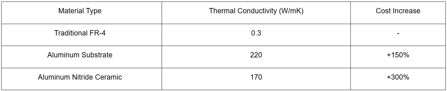
Ⅱ. The Next Decade: Four Application Scenarios Driving Demand
1. The "Hunger Games" of AI Chips
NVIDIA’s H100 GPU requires 6-layer IC Substrate PCBs, with a single board value exceeding $200. OpenAI predicts that AI chip substrates will account for 32% of the global market by 2030.
2. The Invisible Battlefield of 5G mmWave Devices
Qualcomm’s QTM527 antenna module uses 20-layer HDI substrates to support 28GHz signal transmission, with substrates comprising 18% of single base station costs.
3. The "Nerve Center" of New Energy Vehicles
Tesla’s HW4.0 autonomous driving platform integrates 12 substrates, delivering 72 trillion operations per second (TOPS) while reducing power consumption by 25% compared to HW3.0.
4. Precision Advances in Medical Electronics
Medtronic’s next-gen pacemaker employs flexible IC Substrate PCBs with a thickness of 0.15mm and a bending lifespan exceeding 100,000 cycles.
Ⅲ. Chinese Companies’ Path to Breakthroughs
Although Japanese and Korean firms still hold 70% of the global market share (Prismark 2023 data), domestic players like Shennan Circuits and Xingsen Technology have made strides:
1. Substrate yield increased from 65% (2018) to 89% (2023)
2. Mass production capacity for 10+ layer high-end products surpassed 500,000 units/month
3. R&D investment rose from 3.2% (2020) to 7.8% (2023)
Ⅳ. Closing Thoughts: Survival Rules in the Era of Technological Iteration
As Moore’s Law approaches physical limits, innovation in IC Substrate PCBs will become a key variable in sustaining semiconductor progress. To carve a share in the $15 billion market, companies must conquer three critical challenges:
1. Breakthroughs in 8/8μm line width/spacing processes
2. Development of high-frequency materials with Tg above 120°C
3. Establishment of a digital closed-loop system from design to mass production
This micron-level precision race may determine the power dynamics of the global semiconductor industry over the next decade.
IC Substrate The Invisible Cornerstone of High-Density Electronics
IC Substrate PCB From Smartphones to AI Chips—Unveiling the Core Driver of a $100 Billion Market

