


Engineering Guide to Halogen-Free PCBs Technical Depth and Environmental Practices
As global environmental regulations tighten and consumer electronics demand evolves, Halogen-Free PCBs (Halogen-Free Printed Circuit Boards) are becoming a critical technology in electronics manufacturing. According to the IPC-4101B standard, halogen-free PCBs require chlorine (Cl) and bromine (Br) content below 900ppm each, with a total sum not exceeding 1500ppm. This article explores the engineering practices of halogen-free PCBs from three dimensions: material selection, manufacturing processes, and performance validation.

Ⅰ. Core Material Innovations in Halogen-Free PCBs

1. Flame Retardant Alternatives
Traditional PCBs rely on brominated epoxy resins (e.g., TBBPA) for flame retardancy, but these release carcinogens during combustion. Halogen-Free PCBs adopt phosphorus-based (e.g., DOPO) or nitrogen-based flame retardants, enhancing safety through condensed-phase flame retardant mechanisms. Experimental data show that phosphorus-based retardants achieve UL94 V-0 fire resistance ratings for PCBs while raising the thermal decomposition temperature (Td) to above 320°C (Journal of Applied Polymer Science).
2. Substrate Performance Optimization
The key challenge for halogen-free substrates lies in maintaining electrical performance. For example, Panasonic’s MEGTRON6 exhibits a dielectric constant (Dk) of 3.7 at 1GHz and a dielectric loss (Df) of 0.002, representing a 40% improvement in high-frequency performance compared to traditional FR-4 (Dk 4.5, Df 0.02). Additionally, halogen-free materials require a glass transition temperature (Tg) ≥150°C to ensure dimensional stability during high-temperature soldering.
Ⅱ.Manufacturing Process Challenges for Halogen-Free PCBs
1. Adjustments to Lamination Processes
Halogen-free resins exhibit lower fluidity, necessitating adjustments to lamination parameters. Typical optimizations include:
①Temperature: Increased from 170°C to 185°C to ensure full resin flow;
②Pressure: Raised to 400psi to prevent interlayer voids (IPC Technical Report);
③Time: Extended to 120 minutes to enhance crosslinking density.
2. Drilling and Surface Finishing
Halogen-free materials are harder, increasing drill bit wear rates by 15%-20%. Diamond-coated drill bits and spindle speeds of 180,000 RPM are recommended to reduce burring. Surface finishes such as Immersion Silver or ENIG (Electroless Nickel Immersion Gold) are preferred over traditional OSP (Organic Solderability Preservative) for superior oxidation resistance and RoHS compliance.
Ⅲ.Performance Validation and Industry Standards
1. Reliability Testing
①Thermal Stress Test: Per IPC-TM-650 2.6.8, halogen-free PCBs must withstand three 288°C solder dips (10 seconds each) without delamination;
②Humidity Aging: After 168 hours at 85°C/85%RH, insulation resistance must exceed 1×10^8Ω (*IEC 61249-2-21*).
2. Electrical Performance Comparison
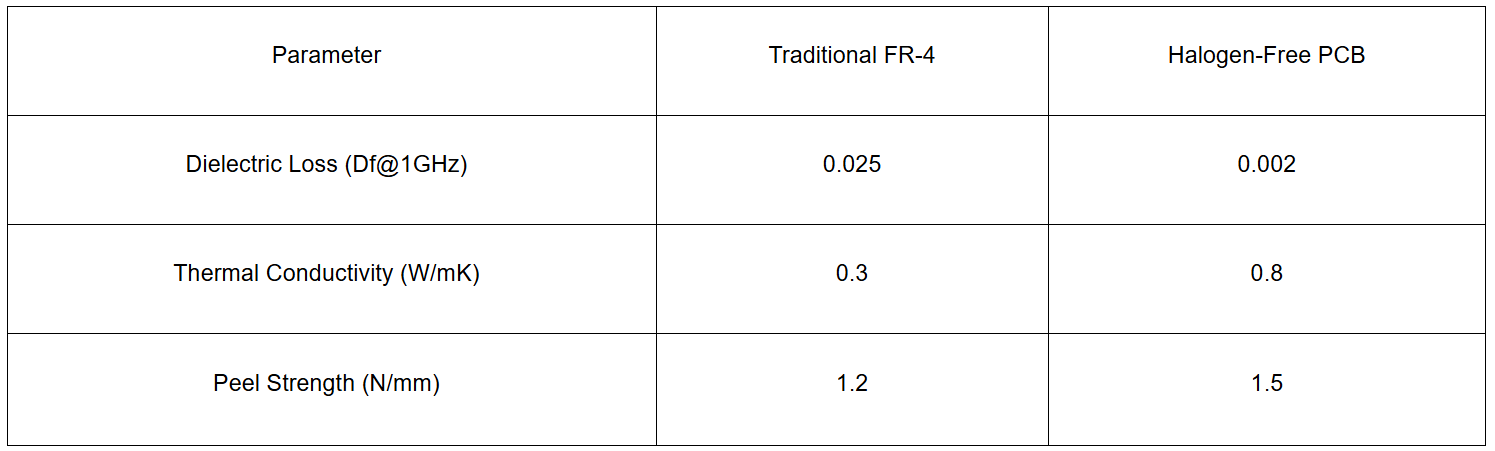
(Data indicate that Halogen-Free PCBs excel in high-frequency performance, thermal management, and mechanical strength, making them ideal for 5G base stations and automotive electronics.)
Ⅳ.Typical Applications of Halogen-Free PCBs
1. Consumer Electronics: Smartphone Motherboards
The Apple iPhone 14 Pro uses Halogen-Free PCBs to reduce motherboard thickness to 0.4mm while passing 30 drop tests (1.2-meter height). High-frequency signal loss is reduced by 30%, significantly improving 5G signal integrity.
2. New Energy Vehicles: Battery Management Systems (BMS)
Tesla’s Model Y BMS module employs 6-layer Halogen-Free PCBs, extending the operating temperature range to -40°C~150°C and lifespan to 15 years in humid environments (vs. 10 years for traditional PCBs).
Ⅴ.Future Trends: Technological Evolution of Halogen-Free PCBs
1. Nano-Filler Technology: Adding silica nanoparticles (<50nm diameter) can boost thermal conductivity to 2.5W/mK while maintaining Df <0.0015 (ACS Applied Materials & Interfaces).
2. Bio-Based Resins: DuPont’s soy-based epoxy resin reduces carbon footprint by 40% and meets UL94 V-0 standards.
Conclusion: The Engineering Value of Halogen-Free PCBs
Halogen-Free PCBs are not only a necessity for environmental compliance but also a cornerstone of high-performance electronics. Through material innovation, process optimization, and rigorous validation, engineers can balance performance and cost to drive sustainable industry growth. As EU CE certification and California’s Proposition 65 gain traction, halogen-free technology will rapidly expand into industrial, medical, and aerospace applications.
Product Applications of Halogen-Free PCBs Technological Breakthroughs and Market Practices
The Future Market of Halogen-Free PCBs Technological Innovation and Trillion-Dollar Opportunities

