


Mastering 2+N+2 HDI PCB Stackup: The Ultimate Guide to High-Density Designs
As the demand for smaller, faster, and more powerful electronic devices grows, traditional PCB designs are being pushed to their limits. HDI (High-Density Interconnect) PCBs have emerged as a solution, offering a way to pack more components into smaller spaces without compromising performance. HDI technology uses finer lines, microvias, and optimized layer structures to handle high-speed signals, reduce interference, and improve overall reliability.
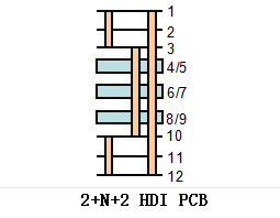
One of the most effective HDI designs is the 2+N+2 stackup. This design consists of two thin outer buildup layers, a customizable number of core layers in the middle (N), and two more buildup layers at the bottom. The structure is highly versatile, allowing engineers to create compact, high-performance circuits while maintaining signal integrity and minimizing electromagnetic interference (EMI). Whether for mobile devices, medical implants, or 5G applications, the 2+N+2 stackup is an ideal choice for modern, high-density electronics.
What is the 2+N+2 HDI Stackup?
Structure and Composition of the 2+N+2 Stackup
The 2+N+2 HDI stackup refers to a specific design structure used in HDI PCBs. In simple terms, this stackup is made up of three main sections: two outer layers, a number of inner core layers, and two more outer layers. Here's a breakdown:
Two outer buildup layers (Top and Bottom): These are the thinnest layers in the PCB, typically around 2-4 mils thick (0.05–0.1mm). These outer layers are used for surface-mount components, such as chips or connectors. They also serve as the starting and ending points for electrical signals traveling through the PCB.
N core layers: These inner layers are where the majority of the routing happens. The "N" represents the number of core layers, which can vary depending on the design complexity. Most commonly, "N" ranges from 2 to 8 layers, depending on the number of signals and power planes required. Core layers are thicker than buildup layers, usually ranging from 4-8 mils (0.1–0.2mm), and are responsible for carrying power, ground connections, and additional signals.
This layer structure helps create a more compact, efficient, and high-performance PCB by making the most of available space and reducing the need for larger, traditional designs.
How 2+N+2 Addresses Design Challenges
The 2+N+2 stackup design tackles several challenges faced by modern electronics, especially in devices that need to be smaller, faster, and more reliable. Let's explore how it helps solve these issues:
Signal Integrity: With high-speed devices, signals can become distorted due to interference or long paths. The inner layers of the 2+N+2 stackup, particularly the core layers, help mitigate this problem by acting as reference planes for signals. By positioning ground planes next to signal layers, this structure reduces electromagnetic interference (EMI) and crosstalk, ensuring that signals travel cleanly and with minimal noise. For example, in mobile phones or 5G devices, where data transmission speed is crucial, signal integrity is key to maintaining high performance.
Miniaturization: In the past, packing more components onto a single PCB often meant increasing the board’s size. With the 2+N+2 stackup, engineers can use the available space more efficiently by incorporating microvias—tiny holes that connect different layers—allowing for a denser arrangement of components. This ability to pack more functionality into smaller spaces is particularly useful in consumer electronics like smartwatches and medical implants, where size is a critical factor.
Reliability: Electronic devices often face harsh environments, whether from heat, vibration, or external interference. The 2+N+2 design helps address these concerns by using thicker inner layers for better heat dissipation and signal shielding. The core layers help distribute power more evenly, while the outer layers provide protection from external environmental factors. For instance, in automotive electronics or medical devices, where reliability under stress is paramount, this stackup ensures the device performs consistently over time.
Layer Breakdown: Understanding Each Component
Buildup Layers (Top and Bottom)
The buildup layers are the outermost layers of the 2+N+2 HDI stackup and play a crucial role in connecting the external components to the PCB. These layers are where you’ll find surface-mount devices (SMDs) like chips and resistors.
Purpose and Functionality of Buildup Layers:
The buildup layers serve as the starting and ending points for signals. They provide a surface for components to be attached and help route signals between components on the outer surface and the inner layers. They are designed to support high-speed signal paths and keep components securely attached.
Thickness, Material, and Copper Weight Specifications:
The buildup layers are typically 2-4 mils (0.05–0.1mm) thick, making them thin yet durable. The copper weight in these layers is usually 0.5–1 oz per square foot (17.5–35µm), balancing current-carrying capacity with signal integrity. Materials used for these layers often include RCC or Ajinomoto ABF, both optimized for laser drilling and fine trace etching.
Role in Microvia Interconnection and Routing:
Microvias—tiny holes drilled using lasers—connect the outer buildup layers to the inner core layers. These microvias reduce the need for larger, traditional vias, helping save space and keep the signal path as short as possible. For example, in a smartphone, these microvias can connect a signal trace on the surface to a ground plane within the core layers, improving signal performance and reducing signal loss.
Core Layers (N)
The core layers sit in the middle of the 2+N+2 stackup and are responsible for carrying signals, power, and ground planes. These layers are thicker than the buildup layers and provide the necessary structure and strength to the PCB.
Core Materials: FR-4 vs. High-Frequency Materials:
Most core layers are made from FR-4, a common material for standard PCBs that offers a good balance of cost and performance. However, for high-speed or high-frequency applications (like 5G or radar systems), materials like Rogers 4350B or Isola I-Tera MT40 are used, offering lower signal loss and better high-frequency performance. The choice of core material depends on the specific needs of the device, balancing cost and signal performance.
Thickness and Copper Weight Considerations for Signal Power Distribution:
Core layers typically range from 4-8 mils (0.1–0.2mm) in thickness, depending on the design complexity and the number of layers. The copper weight for core layers is generally 1-2 oz per square foot (35–70µm), which is heavier than buildup layers. This heavier copper weight ensures that the core layers can support high currents for power distribution and ground connections, essential for maintaining a stable power supply and reducing voltage fluctuations.
Power and Ground Plane Functionality:
Core layers are critical for distributing power and ground connections. In a well-designed stackup, you’ll often find dedicated layers for power planes and ground planes within the core. These planes create a stable reference for signals, preventing interference and helping reduce EMI. For instance, placing a ground plane directly adjacent to a signal layer helps create a shielding effect, which minimizes crosstalk and improves the overall signal integrity of the design.
Layer Interaction and Synergy
The true strength of the 2+N+2 HDI stackup lies in how its layers work together to provide a balance of performance, reliability, and space efficiency.
How Layers Collaborate to Minimize Crosstalk and Enhance Signal Quality:
The buildup and core layers collaborate to reduce signal interference. By strategically placing signal layers next to ground planes in the core, engineers can create a shielding effect that significantly reduces crosstalk (signal interference between different traces). This setup is essential in high-speed designs, such as in 5G devices, where even minor interference can degrade performance.
Role of Core Layers in Heat Management:
The core layers also play a vital role in managing heat. As high-power components like processors generate heat, the thicker core layers act as heat sinks, drawing thermal energy away from these components. In a well-designed 2+N+2 stackup, thermal vias connect the hot components to the core, allowing the heat to spread evenly and preventing overheating. For example, in automotive or industrial applications, this helps ensure that devices perform reliably under high-stress conditions.
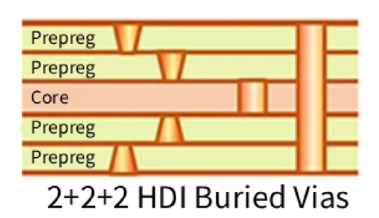
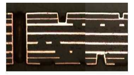
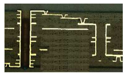
Microvia Technology in 2+N+2 Stackups
Microvia Types and Their Applications
Microvias are tiny holes drilled in the PCB to connect different layers, allowing for more compact and efficient designs. In the 2+N+2 HDI stackup, microvias are essential for creating high-density connections between layers. There are several types of microvias:
Blind Microvias:
Blind microvias connect the outer buildup layers to the core layers, but they do not pass through the entire board. They are perfect for routing signals from surface components to internal layers, helping maintain a compact design. For example, in a smartphone, a blind microvia might route a signal from a surface-mounted chip to a power plane within the core layers, keeping the PCB small and efficient.
Buried Microvias:
Buried microvias connect only the internal core layers of the PCB, and they do not reach the outer surfaces. These microvias are typically used in complex designs where signals need to travel between different core layers. In advanced applications like medical implants or high-performance computing devices, buried microvias help route signals without interfering with the surface layer, allowing for greater flexibility in PCB design.
Stacked Microvias:
Stacked microvias involve two or more microvias stacked vertically to connect non-adjacent layers. This type of microvia is especially useful in ultra-dense PCBs, such as 12-layer BGAs (ball grid arrays) used in high-end smartphones or server boards. Stacked microvias enable multiple connections in a small area, making it possible to fit more components into the same footprint without compromising performance.
Staggered Microvias:
Staggered microvias are offset from each other, meaning they are not aligned vertically. This type of microvia helps reduce mechanical stress, which is important for applications exposed to vibrations, such as in automotive electronics or aerospace devices. By staggering the vias, the PCB becomes more durable and resilient to external forces while still maintaining high-density routing.
Manufacturing Methods: Laser Drilling vs. Mechanical Drilling
The precision and efficiency of microvia construction heavily depend on the manufacturing method used to drill the vias. The two main methods are laser drilling and mechanical drilling, with each offering distinct advantages.
Why Laser Drilling is Preferred for Microvia Construction:
Laser drilling is the preferred method for creating microvias in HDI designs, especially in the 2+N+2 stackup. Laser drilling uses focused laser beams to create precise, clean holes in the PCB, even in the thinnest layers. The main advantage of laser drilling is its ability to produce microvias as small as 0.05mm (2 mils), which is far beyond the capabilities of traditional mechanical drilling. This high precision is essential for HDI designs, where small vias are necessary to maximize space and ensure signal integrity. For example, laser drilling is used in 5G devices to create the tiny vias that connect high-speed signals between layers with minimal loss or interference.
Precision, Cost, and Performance Considerations:
While laser drilling offers high precision, it comes with higher upfront costs due to the need for specialized equipment. However, the cost per unit tends to decrease with larger production runs, making it more cost-effective for high-volume manufacturing. In contrast, mechanical drilling is cheaper upfront, but it is not suitable for creating the small, precise holes required for microvias in advanced HDI designs. Mechanical drilling can create vias as large as 0.2mm (8 mils), which is too wide for many modern applications. In contrast, laser drilling can produce much smaller and more consistent vias, which is crucial for devices where space and signal quality are paramount, such as smartphones or medical electronics.
Benefits of the 2+N+2 HDI Stackup for High-Performance Designs
High Component Density
One of the key advantages of the 2+N+2 HDI stackup is its ability to achieve high component density. This means that more components, such as chips, resistors, and capacitors, can fit into a smaller space compared to traditional PCB designs.
Achieving up to 50% More Components in the Same Footprint Compared to Traditional Designs:
The 2+N+2 stackup allows engineers to reduce the size of the board while still fitting more functionality. This is made possible by the use of microvias, which are much smaller than traditional vias, enabling components to be placed closer together. As a result, designs can support up to 50% more components in the same area compared to older PCB designs. For example, in smartphones, this high-density design enables more powerful processors, larger batteries, and additional features without increasing the size of the device.
This high component density is especially important for devices like wearable technology or medical implants, where space is limited but high performance is required.
Superior Signal Integrity and Noise Mitigation
The 2+N+2 stackup significantly improves signal integrity and reduces the impact of EMI, both of which are critical for high-speed and high-performance electronics.
EMI Reduction and Signal Integrity Advantages:
In high-speed devices like 5G smartphones or data centers, EMI can disrupt signal quality and cause data loss. The 2+N+2 HDI stackup reduces EMI by positioning signal layers next to ground planes within the core layers. This design creates a shielding effect that minimizes interference between signals and prevents them from mixing with unwanted noise.
Additionally, the stackup’s use of microvias helps maintain shorter signal paths, reducing the likelihood of signal degradation. For example, in autonomous vehicles, where split-second decisions are made based on sensor data, ensuring clean and fast signal transmission is critical to system performance and safety.
Space Optimization for Compact Devices
In today’s electronics market, there is an ongoing demand for smaller, lighter devices that still offer top-tier performance. The 2+N+2 HDI stackup is designed to optimize space while maintaining performance, making it ideal for compact and high-performance designs.
How the 2+N+2 Stackup Supports Miniaturization Without Sacrificing Performance:
The 2+N+2 stackup allows for miniaturization by reducing the overall size of the PCB while still offering high-density interconnections. The use of microvias, thinner outer layers, and optimized core layers means that more components can be placed in the same area, all while keeping the design efficient and functional.
Comparing 2+N+2 HDI with Other Stackups
2+N+2 vs. 1+N+1 HDI
When comparing the 2+N+2 HDI stackup to the 1+N+1 HDI stackup, the main differences lie in signal integrity, cost, and performance.
Signal Integrity:
The 2+N+2 stackup provides superior signal integrity compared to the 1+N+1 design. The 2+N+2 stackup uses two outer buildup layers (top and bottom) and core layers that enable better routing options and reduced signal loss. In contrast, the 1+N+1 stackup has only one buildup layer on each side of the core, which limits routing flexibility and increases the chances of signal interference. This makes the 2+N+2 design more suitable for high-speed applications like 5G or autonomous vehicles, where clean and fast signal transmission is crucial.
Cost:
The 1+N+1 stackup is generally more cost-effective than the 2+N+2 stackup due to fewer layers and simpler construction. However, the 2+N+2 stackup offers better performance and higher component density, which may justify the additional cost for high-performance or miniaturized devices. For example, consumer electronics like smartphones often opt for 2+N+2 HDI stackups to balance cost and performance.
Performance Comparison:
The 2+N+2 stackup is ideal for applications that demand high performance in smaller spaces, such as medical devices or 5G technology. It provides higher component density, more precise routing, and better heat dissipation compared to 1+N+1. While 1+N+1 is suitable for less complex designs, 2+N+2 shines in high-performance environments.
2+N+2 vs. Full Build-Up (FBU) Stackups
When comparing the 2+N+2 HDI stackup to Full Build-Up (FBU) stackups, the key differences revolve around efficiency and cost-effectiveness.
Efficiency and Cost-effectiveness of 2+N+2:
The 2+N+2 stackup offers a great balance of performance and cost. While FBU stackups typically have more layers (e.g., 4+4+4 or more), making them ideal for extremely complex designs (like aerospace or supercomputing), they also come with higher manufacturing costs and longer production times. On the other hand, the 2+N+2 stackup offers high component density, superior signal integrity, and miniaturization benefits at a lower cost. For example, a smartphone might use 2+N+2 to provide high performance without the added expense and complexity of a full build-up design.
Cost:
FBU stackups are generally more expensive than the 2+N+2 stackup due to the higher number of layers and the more complex manufacturing process. For applications where the highest performance is required, such as satellite systems or supercomputers, FBU might be necessary. However, for most consumer electronics and industrial devices, 2+N+2 strikes a better balance between cost and performance.
2+N+2 vs. Traditional Multi-layer PCBs
Traditional multi-layer PCBs (8 layers or more) are widely used in industrial and consumer electronics. However, the 2+N+2 HDI stackup provides several key advantages when it comes to design density, performance, and cost.
Design Density:
The 2+N+2 stackup allows for much higher component density than traditional multi-layer PCBs. By using microvias and optimizing layer arrangements, 2+N+2 can fit 50% more components in the same footprint as traditional designs. This makes it ideal for compact devices like smartphones or wearables, where space is limited but performance cannot be sacrificed. Traditional multi-layer PCBs, on the other hand, require larger spaces for components, leading to bulkier designs.
Performance:
In terms of performance, the 2+N+2 stackup excels due to its improved signal integrity and better EMI reduction. By having more layers and better layer stacking (with dedicated signal, power, and ground planes), the 2+N+2 stackup reduces signal loss and interference compared to traditional PCBs. For example, in high-speed applications such as 5G or advanced medical electronics, 2+N+2 ensures that signals travel cleanly and quickly across the board.
Cost:
Traditional multi-layer PCBs might be less expensive in terms of raw materials, but the overall manufacturing cost can increase with more complex designs. In contrast, the 2+N+2 stackup provides higher performance without significant cost increases. In mass production, the cost difference becomes smaller, making the 2+N+2 stackup more cost-effective for advanced electronics.
Comparison Table: 2+N+2 vs. Other Stackups
| Feature | 2+N+2 HDI | 1+N+1 HDI | Full Build-Up (FBU) | Traditional Multi-layer PCB |
| Signal Integrity | Excellent | Good | Excellent | Moderate |
| Cost | Moderate | Low | High | Low |
| Performance | High | Moderate | Very High | Moderate |
| Component Density | High (up to 50% more) | Medium | Very High | Low |
| Complexity | Moderate | Low | High | Moderate |
| Ideal for | 5G, medical, consumer electronics | Basic IoT, simple devices | Aerospace, supercomputing | Industrial, low-speed devices |
Materials Selection: Choosing the Right Core and Buildup Materials
Core Materials for Optimal Performance
The core material of a PCB plays a vital role. Choosing the right material is crucial depending on the application, whether it’s consumer electronics, 5G communication, or data centers.
FR-4: Cost-Effective for Low-Speed Designs
FR-4 is the most commonly used PCB core material. It’s an epoxy resin reinforced with fiberglass, making it highly cost-effective. FR-4 is ideal for low-speed designs where high signal integrity is not as critical. It’s commonly used in household electronics, industrial controls, and basic consumer products. FR-4 offers good dielectric properties and is suitable for most low-frequency applications.
Rogers 4350B: High-Performance Material for 5G and High-Frequency Designs
Rogers 4350B is a high-frequency core material known for its low signal loss and high thermal stability. It’s used in applications that require high-speed signal transmission, such as 5G technology, radar systems, and high-frequency communication. This material offers excellent dielectric constant (Dk) properties, which ensures that signal integrity is maintained at high frequencies. Rogers 4350B is the preferred choice for 5G designs and high-performance communications due to its ability to minimize signal degradation over long distances.
Isola I-Tera MT40: Ideal for Data Centers and 10Gbps+ Signals
Isola I-Tera MT40 is designed for high-speed data communication and is an excellent choice for data centers and systems that handle 10Gbps+ signals. It offers low signal loss and outstanding thermal performance, making it perfect for applications where data integrity and reliability are essential. For example, server farms and high-speed networking devices benefit from I-Tera MT40 because it ensures consistent performance in high-demand environments.
Comparison Table: Core Materials
| Core Material | Performance | Ideal Use Cases | Cost |
| FR-4 | Moderate signal integrity | Low-speed applications (IoT, consumer electronics) | Low |
| Rogers 4350B | High-performance, low loss | 5G communication, radar, high-frequency applications | High |
| Isola I-Tera MT40 | Excellent signal integrity | Data centers, 10Gbps+ networking | Medium |
Buildup Materials and Their Impact
The buildup layers of a PCB are crucial for supporting the routing of signals and connecting components through microvias. The material selection for these layers impacts the board’s signal speed, cost, and flexibility.
Resin-Coated Copper (RCC): Cost-Effective Option for Consumer Electronics
Resin-Coated Copper (RCC) is a common material used in buildup layers for low-cost consumer electronics. It combines a thin layer of resin with copper, providing a good balance of conductivity and cost-effectiveness. RCC is ideal for smartphones, tablets, and consumer appliances where performance and cost must be balanced. While it offers moderate signal performance, it works well for devices with lower signal speed requirements. Its ability to withstand the high temperatures during laser drilling also makes it suitable for microvia applications in consumer electronics.
Ajinomoto ABF: High-Performance Material for Ultra-High-Speed Signals
Ajinomoto ABF (Ajinomoto Build-Up Film) is a high-performance buildup material known for its low signal loss and high-frequency performance. It is widely used in 5G communications, data centers, and other applications that require ultra-high-speed signal transmission. ABF provides excellent dielectric properties, which ensure that the board performs well under high-speed conditions. This material supports fine-pitch component placements and high-density designs, making it ideal for complex PCB applications where precision and signal clarity are critical.
Comparison Table: Buildup Materials
| Buildup Material | Performance | Ideal Use Cases | Cost |
| Resin-Coated Copper (RCC) | Moderate signal integrity | Consumer electronics, low-speed applications | Low |
| Ajinomoto ABF | High-performance, low loss | 5G devices, high-speed networking | High |
Best Practices for Designing a Reliable 2+N+2 HDI Stackup
Stackup Planning and Layer Pairing
Proper stackup planning is the foundation of any successful HDI PCB design. Here, symmetry, impedance control, and layer pairing play key roles in the stackup’s performance and longevity.
Maintaining Symmetry in Buildup Layers to Prevent Warping
Maintaining symmetry between the top and bottom buildup layers is crucial to avoid warping during the manufacturing process. Warping can occur when there’s an uneven pressure distribution across the PCB during lamination or due to differences in material thickness. To prevent this, ensure that the top and bottom buildup layers are of equal thickness. This balanced approach helps keep the board flat and stable throughout its lifecycle, preventing issues like misalignment during assembly or inconsistent performance.
Proper Pairing of Signal and Ground Layers for Impedance Control
Impedance control is essential for signal integrity, particularly in high-speed designs. One key method for achieving impedance control is by pairing signal layers with ground planes. By placing ground planes adjacent to signal layers, you create a stable reference for the signal, helping to minimize crosstalk and EMI. For example, in a 2+4+2 stackup, ensure that each signal layer is paired with a ground plane in the inner core. This arrangement will help control signal propagation and maintain a consistent impedance (often targeted at 50Ω for most high-speed digital signals).
Microvia Design Considerations
Microvias are essential to the dense interconnections in a 2+N+2 HDI stackup. Proper design and manufacturing of microvias are critical for signal integrity, mechanical strength, and reliability.
Aspect Ratio and Spacing Guidelines for Reliability
The aspect ratio of a microvia is the ratio between its diameter and its depth. A higher aspect ratio (meaning a smaller diameter for a greater depth) can lead to manufacturing challenges and reliability issues. Ideally, keep the aspect ratio below 1:1 to ensure that the microvia can be properly filled with copper during plating, maintaining electrical reliability. Additionally, microvias should be spaced at least 2x the diameter apart to reduce the risk of short circuits and ensure ease of manufacturing. This spacing helps avoid issues during the plating process and keeps the design from being too dense.
Copper-Filled Microvias for Mechanical Strength
Copper-filled microvias are used to improve the mechanical strength of the board, especially in applications with high vibration or thermal expansion. These microvias are filled with copper after the drilling process, making them stronger and less likely to fail under stress. For applications in industries like automotive or aerospace, where vibration and physical stress are common, using copper-filled microvias enhances the durability and reliability of the 2+N+2 HDI stackup.
Routing Best Practices
The way signals are routed on a PCB impacts both signal quality and board performance. Following proper routing guidelines is key to maximizing signal integrity, minimizing crosstalk, and maintaining impedance control.
Trace Width and Impedance Control for High-Speed Signals
For high-speed signals (like USB 3.0 or HDMI), trace width plays a crucial role in controlling the impedance. To maintain a consistent impedance (typically 50Ω), trace width must be precisely calculated based on the PCB’s material and thickness. A narrower trace may be needed to maintain high-frequency performance, while wider traces may be used for power or lower-frequency signals. Tools like Impedance Calculators can help ensure that the traces meet the necessary impedance standards, reducing the risk of signal degradation and improving overall signal integrity.
Guidelines for BGA Fan-Out and Differential Pair Routing
BGA (Ball Grid Array) fan-out is a critical area in high-density designs. Proper routing around the BGA pads is necessary to ensure that signal paths are short and even. Use staggered microvias for the fan-out to allow more routing space underneath the BGA and to prevent signal interference from high-density pads. For differential pairs (like those used in USB 3.0 or Ethernet), it’s important to keep the pair's trace width consistent and maintain a precise spacing (typically 5 mils) between the traces. This ensures that the differential pair maintains a balanced impedance and minimizes crosstalk between the lines.
Conclusion: Leveraging 2+N+2 HDI for Advanced Electronic Systems
The 2+N+2 HDI stackup is a game-changer for modern electronics, providing the ideal balance of performance, miniaturization, and cost-efficiency. With its advanced layer structure, this stackup enables designers to pack more components into smaller spaces while ensuring high signal integrity and reliability. It meets the growing demand for compact, high-performance devices by addressing key challenges in signal routing, thermal management, and EMI.
Understanding the intricacies of the 2+N+2 HDI stackup is essential for implementing it successfully in your PCB designs. By optimizing the use of microvia technologies and layer configurations, you can achieve a more efficient design, lower production costs, and better signal quality. For businesses aiming to push the boundaries of electronics, PCBMASTER is an ideal partner. With over a thousand global clients and a proven track record, PCBMASTER offers cutting-edge HDI PCB solutions (4-layer 1-level to 128-layer Any-level HDI PCBs), including rapid prototyping, cost-effective pricing, and fast delivery.
FAQs
How many layers can a 2+N+2 stackup realistically have?
A 2+N+2 stackup can technically support a variety of layer counts depending on the complexity of the design. However, in practice, the N layers typically range from 2 to 8. This gives you stackup options such as 2+2+2 (6 layers), 2+4+2 (8 layers), or 2+8+2 (12 layers). The most common configuration for general applications is the 2+4+2 stackup, providing 8 layers. Beyond this, the design becomes more complex and costly, with diminishing returns in terms of performance gains. Most advanced applications do well with 8 layers.
Can the 2+N+2 stackup handle high-power applications like industrial inverters?
Yes, the 2+N+2 stackup can handle high-power applications, such as industrial inverters, with the proper design adjustments. For high-power scenarios, you can use thicker copper layers (up to 2 oz) in the core to improve current capacity. Additionally, thermal vias can be implemented to help dissipate heat generated by power-hungry components. For industrial inverters and similar applications, 2+4+2 or 2+6+2 stackups are typically used to balance power distribution and thermal management while maintaining signal integrity.
How does 2+N+2 compare in cost to other stackup designs for mass production?
In terms of cost, the 2+N+2 stackup is generally more cost-effective than more complex designs like Full Build-Up (FBU) stackups, which are used in highly specialized applications like aerospace. A 2+N+2 stackup typically costs 30-40% less than FBU stackups while still offering excellent signal integrity and component density. Compared to simpler stackups like 1+N+1, the 2+N+2 is more expensive, but the difference is generally worth it for high-speed designs or applications requiring higher component density and reduced interference. In mass production, the per-unit cost of 2+N+2 designs becomes more competitive, with the difference shrinking to 15-20%.
What’s the minimum order quantity for a 2+N+2 PCB and how does it affect pricing?
The minimum order quantity (MOQ) for a 2+N+2 PCB can vary depending on the manufacturer, but reputable fabricators usually accept prototype orders as small as 1-5 units. For volume production, the MOQ typically starts at 1,000 units or more to qualify for bulk pricing discounts. While the initial cost per unit for low-volume production can be higher, bulk ordering helps reduce the per-unit cost, making 2+N+2 stackups more affordable as production scales. The MOQ often impacts the pricing, as larger volumes lead to lower unit costs due to manufacturing efficiencies.
How do manufacturing processes like sequential lamination impact the final quality of 2+N+2 stackups?
Sequential lamination is a critical process in the 2+N+2 HDI stackup manufacturing. It involves layer-by-layer bonding, where the core layers are first laminated, followed by the outer buildup layers. This process ensures that microvias are aligned properly and that the stackup maintains structural integrity throughout. The quality of sequential lamination impacts the final alignment, layer bonding, and microvia reliability. If the alignment tolerance is not controlled properly (typically ±0.02mm), it can lead to issues like misaligned vias or signal degradation. The use of precise lamination techniques is essential for maintaining the high reliability and performance of 2+N+2 stackups.
Author Bio
Hi, I'm Carol, the Overseas Marketing Manager at PCBMASTER, where I focus on expanding international markets and researching PCB and PCBA solutions. Since 2020, I've been deeply involved in helping our company collaborate with global clients, addressing their technical and production needs in the PCB and PCBA sectors. Over these years, I've gained extensive experience and developed a deeper understanding of industry trends, challenges, and technological innovations.
Outside of work, I'm passionate about writing and enjoy sharing industry insights, market developments, and practical tips through my blog. I hope my posts can help you better understand the PCB and PCBA industries and maybe even offer some valuable takeaways. Of course, if you have any thoughts or questions, feel free to leave a comment below—I'd love to hear from you and discuss further!

