


Common SMD Package Types and Their Uses in Electronics Manufacturing
From compact mobile devices to high-performance computing systems, the performance of modern electronics is shaped not only by circuit design but also by how each component is physically packaged and mounted onto the PCB. These packaging formats are far from arbitrary—they directly influence assembly efficiency, electrical behavior, thermal dissipation, and overall product reliability.
As electronic products continue to shrink while increasing in functionality, engineers must carefully select component packages that balance space constraints with manufacturing practicality and performance demands. This is where Surface-Mount Device (SMD) package types become critical, forming the structural foundation of nearly every modern printed circuit board.
To understand how different devices achieve such varied levels of density, speed, and power handling, it is essential to examine the most common SMD package types used in electronics manufacturing. The following sections break down these package families and highlight how each one is applied in real-world PCB design and production scenarios.
What Are Common Passive SMD Package Types and Their Uses?
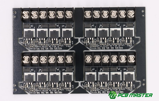
Passive SMD package types refer to the standardized sizes used for surface-mount resistors, capacitors, and inductors. These packages are mainly defined by their physical dimensions rather than complex internal structures. In electronics manufacturing, their main role is to balance board space usage, electrical performance, and assembly reliability. Smaller packages enable higher circuit density, while larger packages support higher power handling and easier assembly.
0201, 0402 packages — Use in ultra-compact mobile and wearable devices
0201 and 0402 SMD packages are used in extremely small electronic products where PCB space is very limited, such as smartphones, smartwatches, and wearable sensors.
0201 (0.6 mm × 0.3 mm) and 0402 (1.0 mm × 0.5 mm) are among the smallest passive SMD components used in modern PCB design. Their main advantage is ultra-high circuit density, allowing designers to fit thousands of components into a very small PCB area.
In real manufacturing, these packages are commonly found in:
· Smartphone RF modules (signal filtering capacitors and resistors)
· Smartwatch power management circuits
· Bluetooth earbuds and IoT sensor nodes
However, they also introduce challenges. Because of their tiny size, they require high-precision SMT placement machines and very accurate solder paste printing. Even slight misalignment can lead to defects like tombstoning or poor solder joints.
In practice, engineers choose 0201/0402 packages when miniaturization is more important than manual repairability or cost simplicity. For example, a smartwatch PCB may use 0402 resistors to save space for battery and antenna design.
0603, 0805 packages — Use in general-purpose consumer electronics
0603 and 0805 SMD packages are widely used in consumer electronics because they offer a good balance between size, cost, and ease of manufacturing.
The 0603 (1.6 mm × 0.8 mm) and 0805 (2.0 mm × 1.25 mm) formats are considered industry-standard passive component sizes. They are large enough to be handled reliably by automated assembly equipment and still small enough to support compact PCB layouts.
Typical applications include:
· LED lighting control boards
· TV and monitor driver circuits
· Laptop and router motherboards
· Home appliances like washing machines and air conditioners
Compared to ultra-small packages like 0402, these sizes are easier to:
· Inspect using AOI (Automated Optical Inspection)
· Rework during repair or prototyping
· Assemble with higher yield in mass production
For example, in a Wi-Fi router PCB, 0603 capacitors are often used in power filtering circuits because they are stable, reliable, and cost-effective.
In manufacturing terms, 0603 and 0805 packages are often chosen when production efficiency and reliability matter more than extreme miniaturization.
1206 and larger packages — Use in power circuits and high-current applications
1206 and larger SMD packages are used in power electronics where higher current, better heat dissipation, and stronger mechanical stability are required.
The 1206 package (3.2 mm × 1.6 mm) and larger sizes are designed for higher power handling capability compared to smaller passive components. Their larger surface area allows better heat distribution, reducing the risk of overheating under load.
Common applications include:
· Power supply circuits in industrial equipment
· Automotive control modules (ECUs)
· LED power drivers and lighting systems
· Motor control and battery management systems
For example, in an electric vehicle battery management PCB, 1206 resistors may be used in sensing and current-limiting circuits because they can handle higher power dissipation without failure.
From a manufacturing perspective, these larger packages are:
· Easier to solder and inspect
· More resistant to vibration and mechanical stress
· Suitable for harsh environments like automotive and industrial systems
However, they take up more PCB space, so engineers usually avoid them in compact consumer devices unless power requirements demand it. In practice, 1206 and larger packages are selected when reliability and power capability are more critical than miniaturization.
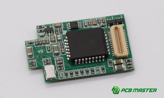
What Are Common Leaded SMD IC Package Types and Their Uses?
Leaded SMD IC package types are integrated circuit packages that use metal leads extending from the body of the chip to connect with PCB pads. These leads are soldered onto the surface of the PCB using SMT (surface-mount technology). In electronics manufacturing, these packages are widely used because they are easy to assemble, inspect, and rework compared to leadless or BGA packages. They are commonly found in analog circuits, digital logic systems, and mixed-signal applications.
SOIC packages — Use in standard analog and digital IC applications
SOIC (Small Outline Integrated Circuit) packages are commonly used for general-purpose analog and digital ICs in consumer and industrial electronics.
SOIC packages feature gull-wing shaped leads on both sides of the chip. These leads make solder joints visible, which improves inspection and quality control in PCB manufacturing.
Typical uses include:
· Operational amplifiers (op-amps)
· Voltage regulators
· Microcontroller peripheral ICs
· Interface chips in consumer electronics
For example, in a simple power supply board, an SOIC-packaged voltage regulator is often used because it is stable, cost-effective, and easy to replace during repair.
From a manufacturing point of view, SOIC packages are preferred when reliability and ease of manual or automated inspection are more important than ultra-compact design. They are also widely used in prototyping because engineers can easily debug solder joints.
SSOP / TSSOP packages — Use in high-density signal and communication circuits
SSOP and TSSOP packages are used in compact electronic designs where more pins are needed in a smaller PCB area, especially in communication and signal processing circuits.
SSOP (Shrink Small Outline Package) and TSSOP (Thin Shrink Small Outline Package) reduce lead pitch compared to SOIC, allowing higher pin density without switching to leadless packaging.
Common applications include:
· Audio codec chips in smartphones and laptops
· Communication ICs in routers and modems
· Memory interface chips (I/O expanders, drivers)
· Signal processing ICs in industrial controllers
For example, a Wi-Fi router PCB may use a TSSOP EEPROM chip to store firmware because it offers a compact footprint while still being easy to assemble and test.
In production, SSOP/TSSOP packages require:
· More precise PCB layout design due to fine pitch leads
· Controlled solder paste printing to avoid bridging
· Proper reflow profile tuning for consistent soldering
These packages are often chosen when designers need higher circuit density but still want easier inspection and lower complexity than BGA or QFN packages.
SOP / PLCC packages — Use in industrial and legacy embedded systems
SOP and PLCC packages are commonly used in industrial electronics and older embedded systems where durability, serviceability, and compatibility are important.
SOP (Small Outline Package) is a broader category of leaded IC packages, while PLCC (Plastic Leaded Chip Carrier) uses J-leads that wrap under the package body, allowing strong mechanical connection to the PCB.
Typical uses include:
· Industrial control boards (PLC systems)
· Automotive electronics (older ECUs and controllers)
· Embedded systems in machinery
· Legacy communication and memory devices
For example, PLCC-packaged microcontrollers are still found in industrial machines because they are durable and easier to replace during maintenance compared to modern fine-pitch packages.
From a manufacturing perspective:
· SOP packages are easier to solder and inspect visually
· PLCC packages provide better mechanical stability under vibration
· Both support easier rework compared to leadless packages
These package types are often selected when long-term serviceability and robustness are more important than miniaturization or ultra-high density design.
What Are Common Leadless SMD Package Types and Their Uses?
Leadless SMD package types are chip packages that do not use external metal leads. Instead, electrical connections are made through flat pads or terminals located directly under or on the bottom of the package. In electronics manufacturing, these packages are widely used in compact, high-performance designs because they reduce signal path length, improve electrical performance, and support better miniaturization. However, they also require more precise PCB design and inspection methods such as X-ray testing.
QFN packages — Use in RF modules, MCUs, and power-efficient IC designs
QFN (Quad Flat No-Lead) packages are used in RF circuits, microcontrollers (MCUs), and power-efficient IC designs where performance, heat dissipation, and compact size are important.
QFN packages have flat contact pads on all four sides and often include an exposed thermal pad at the bottom. This structure helps transfer heat directly into the PCB, improving thermal performance.
Common real-world applications include:
· RF transceivers in Wi-Fi and Bluetooth modules
· Microcontrollers in IoT devices and smart home systems
· Power management ICs in mobile phones and tablets
For example, in a Bluetooth earbud PCB, a QFN-packaged MCU is often used because it saves space while maintaining strong signal performance and low power consumption.
From a manufacturing perspective, QFN packages require:
· Precise solder paste printing to avoid bridging under the package
· Controlled reflow soldering profiles
· X-ray inspection to verify hidden solder joints
QFN is typically selected when high electrical performance and thermal efficiency are required in a compact PCB design.
DFN packages — Use in compact sensors and power management ICs
DFN (Dual Flat No-Lead) packages are used in very small electronic devices such as sensors and power management circuits where space saving and low power consumption are critical.
DFN packages are similar to QFN but usually have fewer pins and a smaller rectangular footprint, making them ideal for ultra-compact PCB layouts.
Typical applications include:
· Temperature and motion sensors in wearable devices
· Battery charging ICs in smartphones
· DC-DC converters in portable electronics
For example, a smartwatch heart-rate sensor module may use a DFN-packaged sensor IC because it minimizes PCB area while maintaining accurate signal performance.
In manufacturing, DFN packages require:
· High-precision SMT placement due to small pad size
· Good solder paste control to prevent voiding
· Careful PCB thermal design to ensure heat flow
DFN packages are often chosen when miniaturization and power efficiency are more important than ease of manual repair or inspection.
LGA packages — Use in high-reliability industrial and communication systems
LGA (Land Grid Array) packages are used in industrial, aerospace, and communication systems where high reliability, stable electrical contact, and strong mechanical performance are required.
LGA packages use a grid of flat contact pads on the bottom of the chip instead of leads or solder balls. The connection is made directly between the package lands and PCB pads.
Common applications include:
· Industrial control systems and PLC modules
· High-performance communication equipment
· Precision sensors in aerospace and defense systems
· Advanced computing and networking hardware
For example, in an industrial automation controller, an LGA-packaged sensor or processor may be used because it can withstand vibration and long-term operation in harsh environments.
From a manufacturing perspective:
· LGA requires very precise PCB alignment during assembly
· X-ray inspection is used to verify solder joint quality
· Rework is more complex compared to leaded packages
LGA packages are typically selected when long-term reliability and electrical stability are more important than low-cost assembly or easy manual repair.
What Are Common BGA-Based SMD Package Types and Their Uses?
BGA-based SMD package types are high-density integrated circuit packages that use an array of solder balls on the underside of the component for electrical connection to the PCB. In electronics manufacturing, these packages are used when a device requires a very large number of input/output (I/O) pins and high electrical performance. Compared to leaded or leadless packages, BGA-based solutions provide better signal integrity, higher routing efficiency, and improved thermal performance, but they require more advanced PCB assembly and inspection processes such as X-ray analysis.
BGA packages — Use in CPUs, GPUs, memory, and high-pin-count ICs
Standard BGA (Ball Grid Array) packages are used in high-performance ICs such as CPUs, GPUs, and memory chips where high pin count and fast signal transmission are required.
BGA packages use a grid of solder balls on the bottom surface of the chip instead of side leads. This structure allows many more connections in a smaller area, making it ideal for complex integrated circuits.
Typical applications include:
· Computer processors (CPU packages in laptops and desktops)
· Graphics processors (GPU chips in gaming systems)
· Memory modules such as DDR RAM and flash storage controllers
For example, a laptop motherboard uses a BGA-packaged CPU because it requires hundreds of high-speed signal connections that cannot be supported by traditional leaded packages.
From a manufacturing perspective:
· Requires precise PCB pad design and alignment
· Needs X-ray inspection to verify hidden solder joints
· Rework is complex and usually requires specialized equipment
BGA packages are selected when high computing performance and dense interconnection are more important than easy repairability.
FBGA packages — Use in advanced computing and high-speed devices
FBGA (Fine-pitch Ball Grid Array) packages are used in advanced computing systems and high-speed electronic devices that require higher interconnection density and faster signal transmission.
FBGA is an improved version of standard BGA with smaller solder balls and tighter spacing, allowing more I/O connections within the same or smaller footprint.
Common applications include:
· High-speed DDR memory modules
· Networking chips in data centers
· High-performance processors in servers
· AI and machine learning accelerator chips
For example, a server motherboard may use FBGA-packaged memory chips to support high data transfer speeds required in cloud computing and AI workloads.
In manufacturing:
· Requires extremely precise PCB fabrication and solder mask alignment
· Sensitive to reflow temperature profiles
· Requires advanced X-ray inspection for defect detection
FBGA is typically used when signal speed and density are more critical than cost or ease of rework.
CSP packages — Use in smartphones, IoT devices, and wearables
CSP (Chip Scale Package) is used in ultra-compact electronic devices such as smartphones, IoT sensors, and wearable electronics where minimizing size is the top priority.
CSP packages are designed so that the package size is almost the same as the silicon die itself, making them one of the smallest BGA-based packaging technologies.
Typical applications include:
· Smartphone processors and memory chips
· IoT sensor modules (temperature, motion, humidity sensors)
· Smartwatch and fitness tracker components
· Compact camera and imaging modules
For example, a smartphone camera module may use CSP-packaged image sensors to fit high-resolution functionality into a very small space.
From a manufacturing perspective:
· Requires extremely high-precision SMT equipment
· Very sensitive to PCB flatness and solder paste control
· Needs X-ray inspection for quality assurance
CSP packages are chosen when ultra-miniaturization and high integration density are more important than ease of assembly or repairability.
Comprehensive Comparison of Different SMD Package Types
Different SMD package types vary mainly in size, electrical performance, thermal capability, manufacturing difficulty, and typical applications. The right choice depends on whether the design priority is miniaturization, power handling, signal speed, or assembly efficiency.
In electronics manufacturing, comparing SMD package types helps engineers quickly decide which package fits a specific PCB design. Below is a structured comparison across the most commonly used categories: passive packages, leaded IC packages, leadless packages, and BGA-based packages.
SMD Package Types Comparison Table
Package Category Typical Package Types Key Strength Main Limitation Common Uses in Electronics Manufacturing Passive SMD Packages 0201, 0402, 0603, 0805, 1206 Simple, low cost, widely available Limited power handling (small sizes) or large PCB space (big sizes) Resistors, capacitors, inductors in all PCB types Leaded IC Packages SOIC, SSOP, TSSOP, SOP, PLCC Easy inspection and rework Larger footprint, lower density Analog ICs, microcontrollers, industrial control boards Leadless IC Packages QFN, DFN, LGA High performance, compact size Difficult inspection and rework RF modules, sensors, power ICs BGA-Based Packages BGA, FBGA, CSP High pin count, excellent signal integrity Complex assembly and inspection CPUs, GPUs, memory, smartphones
| Package Category | Typical Package Types | Key Strength | Main Limitation | Common Uses in Electronics Manufacturing |
| Passive SMD Packages | 0201, 0402, 0603, 0805, 1206 | Simple, low cost, widely available | Limited power handling (small sizes) or large PCB space (big sizes) | Resistors, capacitors, inductors in all PCB types |
| Leaded IC Packages | SOIC, SSOP, TSSOP, SOP, PLCC | Easy inspection and rework | Larger footprint, lower density | Analog ICs, microcontrollers, industrial control boards |
| Leadless IC Packages | QFN, DFN, LGA | High performance, compact size | Difficult inspection and rework | RF modules, sensors, power ICs |
| BGA-Based Packages | BGA, FBGA, CSP | High pin count, excellent signal integrity | Complex assembly and inspection | CPUs, GPUs, memory, smartphones |
How to Interpret This Comparison in PCB Design
Engineers use this comparison to match package type with product requirements such as size, performance, and manufacturability.
For example:
· A smartphone PCB design will use CSP and DFN packages to save space.
· A router or industrial controller may use SOIC or QFN for easier production and repair.
· A laptop motherboard requires BGA packages for CPU and memory due to high pin density.
This structured selection approach helps balance cost, performance, and production yield in electronics manufacturing.
Key Trade-Offs Across SMD Package Types
The main trade-offs are between size, performance, and manufacturability.
· Smaller packages (0201, CSP) → best for miniaturization, hardest to assemble
· Leaded packages (SOIC, TSSOP) → easiest to manufacture, larger footprint
· Leadless packages (QFN, DFN) → best balance of performance and size
· BGA packages → highest performance, most complex inspection and repair
In real PCB production, selecting the wrong package type can lead to:
· Lower assembly yield
· Higher rework cost
· Thermal or signal performance issues
Practical Selection Example (Real Manufacturing Scenario)
In a smart home IoT device design:
· MCU → QFN package (compact + efficient)
· Sensors → DFN package (small + low power)
· Communication chip → BGA package (high-speed data)
· Passive components → 0402/0603 (space + reliability balance)
This combination shows how multiple SMD package types are often used together to optimize overall PCB performance.
How Are Different SMD Package Types Used Across PCB Manufacturing?
SMD package types are not only component formats; they directly affect how a PCB is designed, assembled, and optimized in manufacturing. In PCB production, different package types determine machine settings, thermal behavior, routing density, and overall product reliability. Understanding their role helps engineers improve yield, reduce defects, and optimize cost in SMT assembly lines.
Use in SMT placement and assembly automation
Different SMD package types directly influence SMT placement accuracy, machine speed, and assembly yield in automated PCB manufacturing.
In SMT (Surface Mount Technology) production, pick-and-place machines handle components of different sizes and shapes. Small packages like 0201, DFN, and CSP require high-precision placement, while larger packages like SOIC or 1206 are easier to handle and faster to assemble.
Key impacts in real production:
· Ultra-small packages (0201, CSP) → require high-resolution vision systems and fine nozzles
· Medium packages (0603, QFN, SOIC) → optimized for high-speed mass production
· Large packages (1206, PLCC) → easier alignment, higher mechanical tolerance
For example, in a smartphone SMT line, the same PCB may include CSP memory chips and 0402 passives. The production line must adjust placement speed and inspection settings to avoid misalignment or tombstoning defects.
In practice, engineers select SMD package types based on SMT machine capability, yield targets, and production volume requirements.
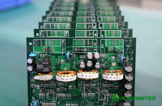
Use in thermal management and power distribution design
SMD package types play a key role in how heat is dissipated and how electrical power is distributed across a PCB.
Different packages handle heat differently depending on their structure and size. In electronics manufacturing, thermal design is critical for reliability, especially in power electronics and high-performance systems.
Key thermal behavior examples:
· QFN packages → use exposed thermal pads to transfer heat into PCB copper layers
· BGA packages → distribute heat across a large solder ball array
· 1206 passive components → handle higher power dissipation than smaller sizes like 0402
Real-world example:
In an electric vehicle battery control board, QFN power ICs are often connected to large copper pours to spread heat efficiently. This prevents overheating during high-current operation.
Design steps commonly used:
1. Select package with adequate power rating
2. Add thermal vias under exposed pads (QFN/LGA)
3. Use wider copper traces for high-current paths
4. Balance component spacing for airflow and heat distribution
Thus, SMD package selection directly affects PCB thermal reliability and power efficiency.
Use in high-density PCB routing and miniaturization strategies
SMD package types determine how densely circuits can be routed and how small a PCB design can become.
Modern electronics require compact PCBs with thousands of connections. Smaller and advanced SMD packages enable tighter routing, while larger packages limit density but improve manufacturability.
Key routing impacts:
· CSP and DFN packages → enable ultra-compact layouts for smartphones and wearables
· QFN packages → reduce routing length and improve signal performance
· SOIC and 0805 packages → require more PCB space but simplify routing design
Example:
A smartwatch PCB uses CSP processors and DFN sensors to fit full functionality into a very small board area, while maintaining battery and antenna space.
Miniaturization strategy steps:
1. Choose smallest viable package for each functional block
2. Use multi-layer PCB routing (4–12 layers typical in compact devices)
3. Minimize trace length for high-speed signals
4. Group passive components in high-density clusters
In summary, SMD package selection is a core factor in achieving high-density PCB design and product miniaturization in modern electronics manufacturing.
Conclusion
From passive components to advanced BGA-based ICs, SMD package types form the structural foundation of modern electronics manufacturing. Each package category plays a specific role—whether it is enabling ultra-compact smartphone designs, supporting high-power industrial systems, or ensuring reliable high-speed computing performance. Understanding these differences allows engineers to make more informed decisions that directly impact PCB size, cost, manufacturability, and long-term reliability.
As electronic products continue to evolve toward higher density and greater functionality, selecting the right SMD package is no longer just a design detail—it is a critical engineering decision that shapes the entire manufacturing outcome. Therefore, a clear understanding of package types and their real-world applications is essential for building efficient and competitive electronic products.
To further support high-quality PCB and PCBA production, experienced manufacturing partners can provide valuable technical guidance and process optimization. In this context, PCBMASTER offers professional PCB fabrication and assembly services designed to help engineers translate design intent into reliable, production-ready hardware with consistent quality and performance.
FAQ About Common SMD Package Types
Which SMD package types are most widely used in electronics?
The most widely used SMD package types are passive packages (0603, 0402), SOIC/TSSOP for ICs, QFN for compact performance chips, and BGA for high-performance processors.
In practical electronics manufacturing, these packages dominate because they balance cost, availability, and assembly reliability. For example, 0603 resistors are standard in consumer electronics, while SOIC and TSSOP packages are common in control circuits. QFN and BGA are used when higher performance or density is required.
Why are BGA packages used in high-performance chips?
BGA packages are used because they support very high pin counts, fast signal transmission, and better electrical performance in compact space.
Unlike leaded packages, BGA uses a grid of solder balls under the chip, allowing hundreds or even thousands of connections. This makes it ideal for CPUs, GPUs, and memory chips where data speed and density are critical. For example, laptop processors rely on BGA packaging to handle high-speed communication between system components.
What SMD packages are best for compact PCB designs?
The best SMD packages for compact PCB designs are CSP, DFN, QFN, and small passive sizes like 0201 and 0402.
These packages minimize footprint while maintaining functionality. For instance, smartphones and wearables often use CSP chips and DFN sensors to reduce board size. QFN is commonly used for MCUs and RF modules because it combines compact size with good thermal and electrical performance.
Which package types are easiest to manufacture and assemble?
The easiest SMD package types to manufacture and assemble are SOIC, 0805/0603 passives, and SOP packages.
These packages have larger pin spacing and visible solder joints, making them easier for SMT machines to place and for engineers to inspect. They also support simpler rework processes. For example, SOIC-packaged ICs are often used in prototypes and industrial boards because they reduce assembly risk and improve yield.
How does package type affect PCB performance and cost?
Package type directly affects PCB size, electrical performance, thermal behavior, and manufacturing cost.
Smaller packages like CSP improve miniaturization but increase assembly difficulty and cost. Larger packages like 1206 or SOIC are easier to assemble but take more PCB space. Advanced packages like BGA improve performance but require X-ray inspection and higher production cost. In practice, engineers balance these factors based on product requirements such as size, speed, reliability, and budget.

