


How AOI Improves PCB Quality: A Complete Guide to Automated Optical Inspection
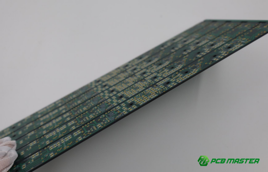
PCB manufacturing is a complex and precise process, where even the smallest mistakes can lead to costly failures. Challenges such as misaligned components, soldering defects, and microscopic surface flaws can compromise the performance and reliability of a printed circuit board. To ensure high-quality output, precise inspection is required at every stage of production.
In this context, Automated Optical Inspection (AOI) plays a critical role. AOI uses high-resolution cameras and intelligent software to quickly and accurately detect defects such as missing components, solder bridges, or misaligned parts. Compared to manual inspection, AOI delivers consistent results, reduces human error, and significantly improves production efficiency.
So, what exactly is AOI, and how does it help improve PCB quality? In the following sections, PCBMASTER will share expert knowledge and hands-on experience to explain how AOI identifies defects, supports continuous process improvement, and helps prevent costly production errors. You’ll also learn how AOI can be applied to consistently manufacture higher-quality PCBs.
What Is Automated Optical Inspection (AOI) in PCB Manufacturing?
Automated Optical Inspection (AOI) is a technology that uses cameras, lighting, and software algorithms to automatically check PCBs for defects during manufacturing, improving accuracy and production efficiency.
Definition and Core Functionality
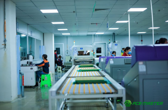
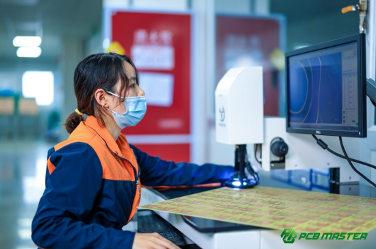
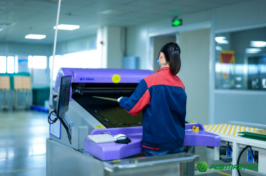
AOI is a system designed to detect defects in printed circuit boards without human intervention. It works by capturing high-resolution images of PCBs as they move along the production line. Bright, controlled lighting ensures that every surface detail is visible, while cameras scan both sides of the board. The captured images are analyzed using intelligent software algorithms that compare the board against its design specifications. This allows AOI to quickly identify problems such as missing components, misaligned parts, or soldering defects. For example, a PCBMASTER production line can spot a tiny solder bridge in seconds, a defect that could be missed during manual inspection.
Key Components of AOI Systems
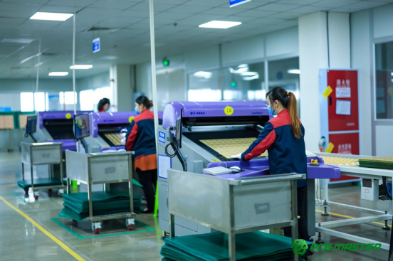
Hardware: The main hardware includes high-resolution cameras, optical sensors, and conveyor systems that move PCBs under the inspection station. Cameras capture detailed images, while sensors detect board position and orientation to ensure accurate scanning.
Software: AOI software is responsible for defect detection. Algorithms analyze images pixel by pixel, comparing them to the PCB design files. Advanced image analysis can detect subtle variations in solder joints or component placement. Some systems even learn from previous inspections to improve accuracy over time.
Together, hardware and software enable AOI to provide consistent, repeatable inspection results, reducing human error and production delays.
Types of Defects AOI Detects
AOI can detect a wide range of defects in PCBs, including:
l Solder Joint Issues: Cold joints, insufficient solder, or bridging between pads.
l Missing Components: Components that were skipped during assembly.
l Misalignments: Components placed incorrectly or rotated out of position.
l Shorts and Opens: Electrical paths that are accidentally connected or disconnected.
For instance, PCBMASTER uses AOI to catch a rotated chip that could cause a device to fail. By automatically flagging such defects, AOI prevents costly rework and ensures higher product reliability. In high-density PCBs, even a tiny misalignment can be detected before the board moves to the next stage, saving time and reducing waste.
How Does AOI Improve PCB Quality Compared to Manual Inspection?
AOI improves PCB quality by providing higher accuracy, faster defect detection, reduced human error, and continuous quality monitoring compared to manual inspection, ensuring more reliable and cost-effective production.
Higher Accuracy and Consistency
AOI provides far more accurate and consistent defect detection than human inspectors. While manual inspection may catch 70–80% of defects on average, AOI systems can detect over 95% of common PCB issues, including tiny solder bridges, missing components, and misalignments. For example, PCBMASTER found that integrating AOI into its production line reduced undetected soldering defects by more than 90% compared to previous manual checks. Unlike humans, AOI does not experience fatigue or attention lapses, ensuring consistent performance across thousands of boards. This high accuracy helps manufacturers deliver higher-quality PCBs and lowers the risk of costly failures in downstream assembly or customer applications.
Faster Detection and Production Flow
AOI accelerates PCB inspection and keeps production flowing efficiently. First, boards move along a conveyor system beneath high-resolution cameras. Next, the AOI software captures images of each board and compares them to design specifications. Defects are flagged automatically within seconds, and defective boards are removed from the line or sent for review. This step-by-step integration allows manufacturers to inspect large volumes of PCBs quickly, reducing bottlenecks in assembly lines. At PCBMASTER, this process enables inspection of hundreds of boards per hour, which would be impossible with manual inspection alone.
Reduced Human Error and Operational Costs
Manual inspection is prone to human error, which can lead to undetected defects and costly rework. AOI reduces these risks by automatically identifying even subtle defects with consistent accuracy. This prevention of errors saves operational costs associated with rework, scrap, and warranty claims. For instance, PCBMASTER estimated that using AOI reduced annual rework costs by 25%, translating into significant savings while maintaining high-quality standards. By detecting problems early, AOI also prevents defective boards from reaching customers, protecting brand reputation.
Continuous Quality Monitoring
AOI enables real-time quality monitoring throughout the PCB production process. Each board is scanned automatically, and inspection data is logged for analysis. This immediate feedback allows production teams to adjust processes quickly—for example, fine-tuning soldering parameters or correcting component placement issues. At PCBMASTER, AOI logs are used to track defect trends over time, enabling proactive process improvements. Continuous monitoring ensures that every board meets quality requirements before leaving the production line, minimizing defects and increasing overall reliability.
What Are the Key Steps in Implementing AOI in PCB Manufacturing?
Implementing AOI in PCB manufacturing involves careful planning, system setup, validation through test runs, and full production integration to ensure accurate, efficient, and continuous defect detection.
Pre-Implementation Planning
Before introducing AOI, manufacturers need to define inspection criteria based on PCB design and production complexity. This includes identifying critical components, sensitive solder joints, and high-density areas that require precise inspection. For example, multilayer PCBs or boards with tiny 0201 components may need stricter detection thresholds. At PCBMASTER, engineers analyze design files and historical defect data to prioritize which areas the AOI system should focus on. Clear planning ensures the AOI system is configured to meet production goals and prevents unnecessary false alarms, improving both efficiency and quality outcomes.
AOI System Configuration
AOI systems must be configured for optimal performance before production. This involves setting up cameras, adjusting lighting to highlight defects without glare, and calibrating software algorithms to recognize acceptable tolerances. For instance, slight variations in solder shape can be normal, and the algorithm must be trained to distinguish these from actual defects. At PCBMASTER, technicians adjust camera angles and illumination patterns for each board type, ensuring the AOI system accurately identifies missing or misaligned components without flagging harmless variations. Proper configuration maximizes detection accuracy from day one.
Test Runs and Defect Benchmarking
After setup, AOI systems undergo test runs to validate detection thresholds. Sample boards are scanned, and detected defects are compared against known errors. PCBMASTER uses this stage to fine-tune sensitivity: if the system misses a small solder bridge or incorrectly flags a minor variation, adjustments are made. This benchmarking ensures that AOI catches real defects while minimizing false positives. These controlled tests establish confidence that the AOI system can handle the full production load without slowing operations or generating unnecessary alerts.
Full Production Integration
Once validated, AOI is integrated into the full production workflow. Boards are inspected in real-time, and defect data is logged automatically. Continuous monitoring allows technicians to track trends, identify recurring issues, and make immediate process adjustments. At PCBMASTER, this integration means that every board is inspected automatically, defects are flagged instantly, and production continues without bottlenecks. Full integration ensures a reliable, high-quality output and allows manufacturers to maintain consistent standards across all batches, from prototypes to high-volume production.
Which Types of PCB Defects Are Most Effectively Prevented by AOI?
AOI is most effective at preventing soldering defects, component placement errors, and surface defects on PCBs, providing faster, more accurate, and consistent detection than manual inspection.
Soldering Defects
Soldering defects are a major source of PCB failures, and AOI is highly effective at detecting them. Common issues include insufficient solder, where the joint does not fully connect the component to the pad; solder bridging, where excess solder creates unintended connections; and cold joints, where the solder does not form a proper bond. AOI systems use high-resolution imaging and lighting to identify these issues instantly. For example, PCBMASTER uses AOI to detect a tiny solder bridge between two pins of a microcontroller, preventing a short circuit that could have caused a product failure. By catching these defects early, AOI ensures higher reliability and reduces costly rework.
Component Placement Errors
AOI can accurately detect errors in component placement, which are often difficult for humans to spot. This includes misaligned components, incorrect polarity for diodes or capacitors, and missing parts that were skipped during assembly. At PCBMASTER, AOI has prevented dozens of potential failures in high-density boards by flagging chips that were rotated 90 degrees or capacitors that were missing entirely. By automatically checking alignment and orientation, AOI helps maintain functional and electrical integrity across all PCBs.
Surface Defects
Surface defects such as scratches, contamination, or oxidation can affect PCB performance and reliability. AOI systems can detect these issues by analyzing surface texture and color under controlled lighting. For instance, AOI at PCBMASTER has identified scratches on protective solder masks and contamination from dust particles before boards entered further assembly. Detecting surface defects early ensures that only fully compliant PCBs continue through production, preventing downstream failures and improving overall quality.
Comparative Table: Manual vs. AOI Detection
Defect Type Detection by Manual Inspection Detection by AOI Notes / Benefits Soldering Defects Medium (may miss small bridges or cold joints) High (detects almost all issues, even microscopic) Reduces short circuits and rework Component Placement Errors Medium-Low (difficult for humans on dense boards) High (accurate alignment, polarity, and presence checks) Prevents functional failures Surface Defects Low (scratches or contamination often overlooked) Medium-High (detects scratches, oxidation, contamination) Ensures PCB reliability and clean assembly
| Defect Type | Detection by Manual Inspection | Detection by AOI | Notes / Benefits |
| Soldering Defects | Medium (may miss small bridges or cold joints) | High (detects almost all issues, even microscopic) | Reduces short circuits and rework |
| Component Placement Errors | Medium-Low (difficult for humans on dense boards) | High (accurate alignment, polarity, and presence checks) | Prevents functional failures |
| Surface Defects | Low (scratches or contamination often overlooked) | Medium-High (detects scratches, oxidation, contamination) | Ensures PCB reliability and clean assembly |
How Can AOI Data Be Used to Continuously Improve PCB Quality?
AOI data can be analyzed to spot recurring defects, optimize manufacturing processes, and provide actionable feedback to design and production teams, helping manufacturers achieve higher and more consistent PCB quality.
Defect Trend Analysis
AOI systems automatically log defect data for every inspected PCB. This data can be analyzed to identify recurring issues in production. For example, if AOI consistently flags misaligned capacitors in a specific board area, it indicates a systematic placement problem. At PCBMASTER, engineers review AOI logs weekly to track defect trends over time. By understanding which defects occur most frequently, teams can prioritize corrective actions, prevent repeat errors, and maintain higher production standards. Defect trend analysis turns raw AOI data into actionable insights for continuous quality improvement.
Process Optimization
AOI insights allow manufacturers to fine-tune production processes. If recurring defects are traced to soldering issues, soldering profiles can be adjusted—such as temperature, dwell time, or flux application. Misalignment trends may indicate pick-and-place machine calibration issues that need correction. PCBMASTER uses AOI data to make precise adjustments to assembly equipment, improving component placement accuracy and solder joint reliability. This proactive optimization reduces rework, minimizes scrap, and ensures a smoother, more consistent production flow.
Feedback Loop for Design and Manufacturing Teams
AOI data also creates a feedback loop between production and design teams. For instance, if AOI frequently flags components that are hard to place or inspect due to tight spacing, PCBMASTER’s design team can adjust the layout in future revisions. Similarly, component selection or pad design can be refined to reduce soldering defects. By integrating AOI insights into both design and manufacturing decisions, teams can prevent recurring issues, streamline assembly, and produce higher-quality PCBs from the start.
Conclusion
Automated Optical Inspection (AOI) improves PCB quality by ensuring faster, more accurate, and consistent defect detection. It prevents soldering flaws, component placement errors, and surface defects, reducing rework and scrap while boosting production efficiency.
At PCBMASTER, we use advanced AOI systems to deliver reliable PCBs and PCBA solutions. Real-time monitoring and intelligent algorithms help us catch defects early, ensuring every board meets high-quality standards.
Integrating AOI is a best practice in modern PCB manufacturing. By adopting AOI, manufacturers can achieve consistent quality, lower costs, and produce more reliable, high-performance PCBs.
FAQ: Automated Optical Inspection in PCB Manufacturing
1. What is the typical defect detection rate of AOI in PCBs?
Automated Optical Inspection (AOI) typically detects over 95% of common PCB defects, including solder bridges, missing components, and misalignments. Compared to manual inspection, which may catch only 70–80% of defects, AOI provides much higher accuracy and consistent results across thousands of boards.
2. Can AOI detect micro-defects in high-density PCBs?
Yes. AOI systems with high-resolution cameras and advanced imaging algorithms can identify micro-defects in high-density PCBs, such as tiny solder bridges or misaligned 0201 components. Proper lighting and calibration are critical to ensure these small defects are reliably detected.
3. How does AOI complement other inspection methods like X-ray inspection?
AOI excels at detecting surface defects and component placement issues, while X-ray inspection is better for hidden defects, like solder voids under BGAs (Ball Grid Arrays). Together, AOI and X-ray provide comprehensive defect coverage, ensuring both visible and hidden flaws are identified.
4. Is AOI suitable for small-batch or prototype PCBs?
Yes. Modern AOI systems can be configured for small-batch or prototype production. Quick setup and flexible inspection criteria allow manufacturers to test prototype boards efficiently, catch defects early, and improve design iterations before mass production.
5. What are the main limitations of AOI and how to mitigate them?
AOI has limitations in detecting hidden defects, like internal solder voids, and can generate false positives if lighting or calibration is incorrect. These can be mitigated by combining AOI with X-ray inspection, regularly calibrating systems, and fine-tuning defect thresholds for each PCB type.

