


Why Some PCB or PCB Assembly Order Need SMD Stencil Shipped With the Order
Introduction
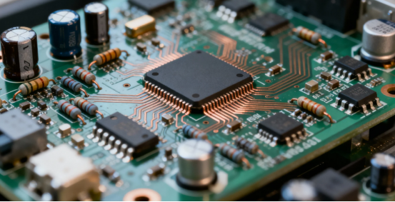
Behind every sophisticated circuit board in modern electronics manufacturing lies a seemingly simple yet crucial tool—the SMD stencil.
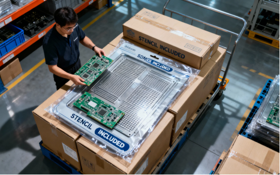
In the PCBA (Printed Circuit Board Assembly) process, one detail often overlooked by non-professionals is that many PCB or PCB assembly orders require the SMD stencil to be shipped together with the order. To those unfamiliar with electronics manufacturing, this might seem unnecessary—why not just start the assembly directly?
What role does this thin piece of stainless steel actually play? SMD stencils are often custom or specially designed for each PCB order to ensure precise solder paste application. Today, we will explore this in detail.
Introduction to PCB Assembly
PCB assembly is a multi-step process that transforms a bare printed circuit board into a fully functional electronic device. One of the most critical steps in this process is applying solder paste to the PCB, which acts as the adhesive and electrical connection for surface mount devices (SMDs). To achieve high precision and repeatability, manufacturers rely on SMT stencils—thin sheets of metal with laser-cut apertures that perfectly match the SMD pads on the board. By using SMT stencils, the process of applying solder paste becomes fast, accurate, and consistent, which not only improves the quality of the final product but also eliminates tedious hand soldering. This is especially valuable in prototype PCB assembly jobs, where time and accuracy are essential. With the help of a toaster reflow oven, the solder paste is melted to form strong, reliable joints, allowing even small-scale projects to achieve professional results. The use of stencils and automated processes ensures that each printed circuit is assembled with the same level of care and precision, making PCB assembly more efficient and less prone to human error.
What Is an SMD Stencil?
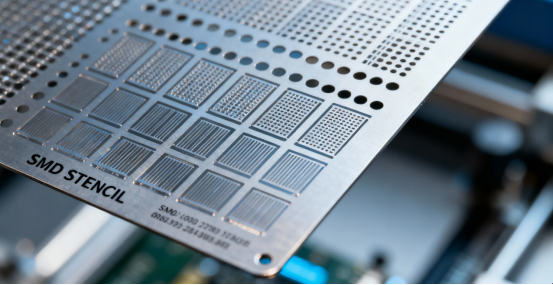
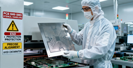
An SMD stencil, also known as an SMT stencil, is a critical tool in Surface Mount Technology. It is a precision-made template from a thin stainless steel foil, commonly produced as laser cut stencils for high precision, featuring small openings that perfectly correspond to the PCB pad locations (sometimes referred to as a pcb stencil).
Think of it like using a stencil with patterned cutouts to sprinkle powdered sugar in a specific design on a cake. The SMD stencil plays a similar role in PCB manufacturing—it uses its openings to accurately print solder paste onto the PCB pads, preparing the board for subsequent component placement and soldering. The top surface of the stencil must make close contact with the PCB to ensure accurate paste deposition.
Types of Stencils
When it comes to PCB assembly, choosing the right type of stencil is crucial for achieving optimal results. There are several types of SMT stencils available, each designed to meet specific production needs. Framed stencils are mounted on a rigid frame, providing stability and durability for high-volume assembly lines where repeated use is required. Frameless SMT stencils, on the other hand, are more cost-effective and ideal for prototype PCB assembly or small batch runs, as they are lightweight and easy to handle. Step stencils offer another level of versatility by allowing different solder paste thicknesses in various areas of the same stencil, which is particularly useful when assembling boards with components of varying heights or paste requirements. The choice between framed, frameless, and step stencils depends on factors such as the complexity of the components, the size of the PCB, and the overall production volume. By selecting the appropriate stencil type, manufacturers can ensure that solder paste is applied accurately and efficiently, supporting a smooth and reliable PCB assembly process.
Why Are Stencils So Critical to the SMT Process?
The Precision Controller for Solder Paste Printing
In the SMT production process, solder paste printing is one of the first and most critical steps. The quality of the stencil directly determines the quality of the solder paste printing—the stencil's thickness, opening size, and shape dictate the amount of paste deposited.
Insufficient solder paste can lead to weak or incomplete solder joints (virtual soldering), while excessive paste can cause bridging and short circuits. Both scenarios severely impact soldering quality, necessitating time-consuming rework and directly affecting the overall efficiency of the board assembly process.
Addressing the Challenges of Electronics Miniaturization
As electronic devices become increasingly compact and powerful, components are also shrinking—0201 imperial components have become mainstream, 01005 imperial (0402 metric) components are increasingly common, and even 03015 metric components are being introduced in new products.
Facing these miniature components, releasing solder paste through the stencil’s very small openings becomes increasingly challenging. At this point, the design and manufacturing quality of the stencil become paramount. It must ensure excellent paste release, even from the finest apertures. Components such as micro BGA and BGA packages require especially precise stencil design and manufacturing due to their fine pitches.
Ensuring Soldering Consistency
In mass production, consistency is a key measure of quality. Using a stencil for solder paste printing ensures that every solder joint on every PCB receives nearly the same amount of paste, laying a solid foundation for the subsequent reflow soldering process. This consistency is vital for improving overall yield rates and reducing debugging and repair efforts.
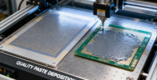
Applying Solder Paste
The application of solder paste is a pivotal step in the PCB assembly process, directly impacting the quality and reliability of the finished product. To apply solder paste with precision, manufacturers use a stencil kit, which typically includes a laser-cut stencil, a squeegee blade, and board holders. The process begins by securely placing the stencil over the printed circuit board, aligning the apertures with the corresponding pads. Using the squeegee blade, solder paste is spread across the stencil, filling the apertures and depositing the paste exactly where it’s needed. Board holders keep the PCB steady, ensuring even and accurate application. Once the solder paste is in place, the board is ready for surface mount components to be positioned. For prototype PCB assembly jobs, a toaster reflow oven is often used to heat the board, melting the solder paste and forming strong, reliable connections. This method streamlines the assembly process, reduces the risk of defects, and delivers high-quality results without the need for tedious hand soldering.
Why Do Some Orders Require Stencils Shipped With Them?
Guaranteeing Process Consistency for Future Production
When a customer needs to place additional orders or perform repairs in the future, using the same stencil ensures the solder paste printing results match the initial production exactly. This is particularly important for long-term projects and products with extended maintenance cycles.
Stencils from different production batches can have subtle variations. Even for the same design, stencils made at different times might differ slightly due to adjustments in process parameters, and these minor differences can affect soldering quality.
Supporting Customer's Secondary Development and Debugging
For R&D-focused companies, retaining the stencil allows them to conduct small-batch trial production or process verification in their own labs or pilot lines, without needing to subcontract to a PCBA factory each time.
When design fine-tuning is required, experienced engineers can even make local modifications to the stencil to accommodate component changes or circuit adjustments, significantly enhancing development flexibility and efficiency.
Reducing Future Production Costs
If the client plans multiple production runs in the future, having their own stencil can avoid recurring rental or fabrication fees for the stencil. While stencil fabrication requires an initial investment, it can actually lower the overall production cost for long-term manufacturing.
Meeting Urgent Production Needs
When urgent product demand arises or sudden failures require quick fixes, having the stencil on hand can significantly shorten production lead times and enable a rapid start to the manufacturing process. In certain scenarios, this can be crucial for ensuring fast market response or timely repairs.
The Art of Stencil Design and Fabrication
Creating high-quality stencils is no simple task; it’s an art combining experience and technology. Tools such as check plots are used to verify stencil designs before fabrication, ensuring accuracy and quality.
Precision Stencil Design
Modern stencil design uses advanced Gerber editing software to precisely calculate aperture area and aspect ratios, reporting whether these ratios fall below given thresholds. Design engineers must determine the optimal foil thickness or decide if a step stencil is needed, based on the PCB layout and component characteristics. Some stencils are specifically designed for unique component layouts or challenging assembly requirements.
Material Selection
Mainstream stencil materials include:
·Fine-grain stainless steel: Materials with a grain structure of 5 microns or smaller. Research indicates that specific "fine-grain" stainless steel technical foils can provide better solder paste release with less variation.
·Electroformed nickel: Crucial for requirements demanding very thin stencils (e.g., 1.5 to 3 mil thin foils).
Process Considerations
Stencil fabrication must account for factors like solder paste type, component pin pitch, and PCB pad design. For instance, high-density assembly boards might require more advanced laser-cutting technologies, achieving precision up to ±15μm.
Stencil Accessories and Options
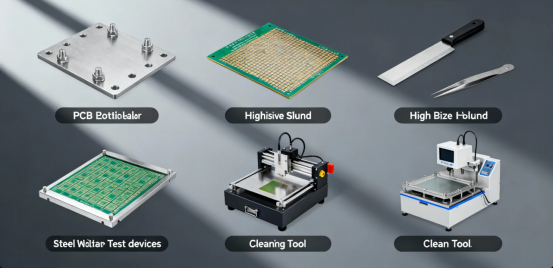
To further enhance the PCB assembly process, a range of stencil accessories and options are available. Stencil cleaning solutions are essential for maintaining the accuracy and longevity of the stencil, as they effectively remove solder paste residues and prevent aperture blockages. Inspection aids, such as check plots, allow manufacturers to verify that the stencil matches the intended design and meets all required specifications before use. Additionally, design assistance services can help optimize stencil layouts, ensuring that the apertures are tailored to the unique needs of each PCB assembly project. By utilizing these accessories and options, manufacturers can uphold high standards of quality, minimize errors, and ensure that every stencil performs at its best throughout the assembly process.
Circuit Board Considerations
When assembling printed circuit boards, several key factors must be considered to ensure a successful outcome. The type of components used—whether they are fine-pitch micro BGAs or larger surface mount devices—will influence the choice of SMT stencil and the solder paste application method. The size and shape of the PCB also play a significant role; larger boards may benefit from framed stencils for added stability, while smaller or uniquely shaped boards might be better suited to frameless stencils. Production volume is another important consideration, as high-volume runs often require more robust stencil solutions, whereas prototypes or small batches can utilize more economical options. By carefully evaluating these aspects, manufacturers can design a PCB assembly process that is both efficient and cost-effective, ensuring that each board meets stringent quality and performance specifications. With the right combination of SMT stencils and thoughtful process planning, high-quality PCBs can be produced consistently, regardless of the complexity or scale of the project.
Key Considerations for Stencil Use and Storage
After receiving the stencil with your order, proper use and storage are equally important:
·Pre-Use Inspection: Before each use, inspect the stencil openings to ensure they are clean, free from residual paste or blockages.
·Proper Cleaning: Clean the stencil thoroughly with appropriate cleaning agents immediately after use to prevent solder paste residue from clogging the apertures.
·Appropriate Storage: Store stencils in a dry, dust-free environment, avoiding bending or impact that could cause deformation.
·Labeling and Record Keeping: Clearly mark the stencil with the corresponding product model, version number, and fabrication date for future traceability.
Future Trends in Stencil Technology
As electronic technology advances, stencil technology continues to evolve:
·Higher Precision: Meeting the challenges of ultra-small 01005 components and 0.3mm pitch BGAs.
·Smarter Design: New stencil design technologies allow engineers to design specific components (like QFNs) considering leads and pads as a whole, storing them in libraries to reduce human error.
·New Material Applications: Development of superior fine-grain stainless steel materials to further enhance solder paste release performance.
Conclusion
In the realm of PCB and PCBA, the SMD stencil, while a seemingly simple tool, plays an indispensable role in the entire production process. It acts as a bridge connecting design and manufacturing, precisely translating design blueprints into physical products.
The next time you see the option for "SMD stencil shipped with order," may you understand the strategic thinking behind it—this isn't just about the physical delivery of a tool, but a strategic decision concerning quality consistency, production autonomy, and long-term cost control.
In an era of increasingly sophisticated and complex electronics, paying attention to "small details" like the stencil often makes a "significant difference" in the final product's quality and reliability.
Have you encountered quality fluctuations in your PCB manufacturing process related to stencil issues? Feel free to share your experiences and insights in the comments section
FAQs
Q. What is an SMD stencil?
A. It's typically a thin metal sheet (often stainless steel) with precisely cut openings that match the PCB pads, used for accurately applying solder paste during SMT assembly.
Q. What are the common types of SMD stencils?
A. Types include laser-cut stencils and electroformed stencils; structurally, there are framed and frameless stencils. For special needs, step stencils (for varying paste volume) and prototype stencils (for sample testing) are also available.
Q. How to choose the right stencil thickness?
A. This depends on the finest component pitch and aperture size. Use 0.15mm for standard boards, 0.2mm if more paste is needed. For components below 20-mil pitch, use 0.125mm; micro BGAs may require 0.1mm. The typical thickness range is 3-8 mils.
Q. What file formats are needed for stencil production?
A. Gerber files are most commonly accepted, though ODB++ and DXF are also supported. It's recommended to provide complete solder paste layer files to avoid repeated modifications.
Q. What is the purpose of stencil coating?
A. Coatings improve paste release, reduce cleaning frequency, and extend stencil life. Common coatings include nano-coatings and gold plating, particularly suitable for high-volume production.
Q. What if solder paste won't release properly from the stencil?
A. Consider surface polishing or specialized coated stencils. Also, promptly clean residual paste from apertures and optimize paste viscosity for the production process.
Q. Can SMD stencils be reused?
A. Yes. After thorough cleaning to remove paste residue and verification that apertures show no deformation or wear, stencils can be reused. Framed stencils generally offer more stable repeated use than frameless versions.
Q. How should SMD stencils be stored?
A. Framed and quick-mount stencils can be shelved. Smaller stencils should be kept in dedicated bags or boxes to prevent aperture damage and surface contamination.
Q. Should aperture sizes exactly match PCB pads?
A. No. For standard components, apertures can be 5%-10% smaller than pads. Fine-pitch components require adjusted aperture widths to maintain proper area ratio and avoid bridging.
Q. Is precise alignment between stencil and PCB necessary during use?
A. Yes. Accurate alignment using fiducial marks is essential. Misalignment causes paste deposition errors, leading to soldering defects like poor joints or bridging.
Author: Jack Wang

