


Optimizing PCB Assembly Line Pad Add Tinning for Enhanced Reliability
Introduction
In the intricate world of PCB assembly (printed circuit board assembly), even minor process details can determine the final quality and lifespan of electronic products. Among these critical details, line/pad add tinning stands out as a seemingly simple yet highly impactful step. Whether you’re an electronics manufacturer striving to reduce production defects, an R&D engineer optimizing PCB designs, or a hobbyist looking to improve your DIY circuit boards, understanding line/pad add tinning is essential.
This article will break down what line/pad add tinning is, why it matters in PCB assembly, its core application scenarios, proper operation methods, common problems and solutions, and future development trends. By the end, you’ll have a comprehensive grasp of this key process and how to leverage it to boost the performance of your PCBs.
What Is Line/Pad Add Tinning in PCB Assembly?
Before diving into the specifics, let’s clarify the basic concepts. In PCB terminology, “lines” refer to the conductive traces on the board that transmit electrical signals and power between components. “Pads” are the small, flat conductive areas designed to connect electronic components (such as resistors, capacitors, and chips) to the PCB, serving as the interface for soldering. The circuit board acts as the foundation for these lines and pads, supporting the overall structure and function of the electronic assembly.
Line/pad add tinning, also known as trace and pad tin-plating or tin deposition, is the process of applying a thin layer of tin (or tin-based alloys like tin-lead or tin-silver-copper) to the surface of PCB lines and pads during assembly. Unlike the initial tinning done during PCB fabrication, this post-fabrication tinning step is tailored to address specific assembly challenges, repair defects, or enhance the solderability and conductivity of key areas.
The tin layer applied in this process is typically thin—ranging from 1–3 microns—but its role is far from negligible. Tin is chosen for this task primarily due to its excellent solderability, corrosion resistance, and cost-effectiveness. It forms a stable bond with solder, ensuring strong and reliable connections between components and the PCB, while also protecting the underlying copper lines and pads from oxidation. Some finishes, such as thick gold plating, can result in poor solderability, making tin a more suitable choice for solderable areas.
It’s important to distinguish line/pad add tinning from other surface finishing processes. For example, HASL (Hot Air Solder Leveling) is a mass-finishing method applied during PCB manufacturing, covering the entire board’s exposed copper. In contrast, add tinning is a targeted process, often applied only to specific lines or pads that need extra reinforcement. The solder mask layer on a circuit board plays a crucial role in protecting the board and preventing solder bridges during these processes. Similarly, ENIG (Electroless Nickel Immersion Gold) offers superior corrosion resistance but is more expensive; add tinning serves as a flexible, cost-efficient supplement or alternative for certain applications.
Why Line/Pad Add Tinning Is Indispensable in PCB Assembly
You might wonder: if PCBs already undergo surface finishing during fabrication, why go through the trouble of adding tin to lines and pads during assembly? The truth is, add tinning solves multiple pain points that often arise in practical production, directly impacting product quality, yield rate, and long-term reliability. Proper tinning practices are essential for ensuring the reliability of pcb assemblies by preventing issues such as pad lifting and poor solder joints.
When considering add tinning for specific scenarios, it's important to select the most suitable tinning process or material based on the application's requirements, compliance standards, and desired performance.
Prevents Oxidation and Improves Solderability
Copper, the primary material for PCB lines and pads, is highly prone to oxidation when exposed to air. Even a thin layer of copper oxide can drastically reduce solderability—during soldering, the solder will bead up instead of spreading evenly, leading to cold joints, poor wetting, or even complete failure to bond. This is especially problematic for PCBs that have been stored for a long time before assembly or exposed to humid environments.
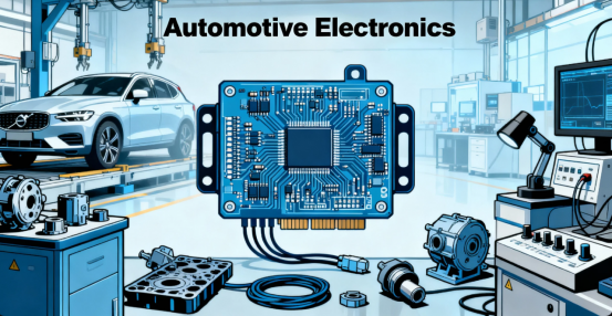
Adding a tin layer acts as a protective barrier. Tin oxidizes much slower than copper, and the thin oxide film on tin can be easily broken down during soldering, ensuring smooth solder flow. For example, in the assembly of automotive electronic control units (ECUs), which often face long storage cycles before installation, line/pad add tinning significantly reduces the risk of soldering defects caused by copper oxidation, ensuring stable performance of critical components.
Strengthens Mechanical and Electrical Connections
In high-vibration environments—such as industrial machinery, aerospace equipment, or automotive electronics—PCB components are prone to loosening due to repeated stress. The tin layer from add tinning enhances the mechanical strength of the solder joints. When solder melts and combines with the tin layer, it forms a denser, more durable intermetallic compound, making the connection more resistant to vibration and thermal expansion.
Electrical performance also benefits. The tin layer improves the conductivity of lines and pads, reducing signal loss and voltage drop—key considerations for high-frequency PCBs used in communication devices. For instance, in 5G base station PCBs, where signal transmission speed and stability are paramount, adding tin to high-current lines ensures consistent power delivery and minimizes interference.
Repairs Manufacturing Defects and Reduces Scrap
Even with strict quality control, PCB fabrication can produce minor defects: a pad with insufficient tin plating, a line with partial copper exposure, or uneven surface finishing. Discarding an entire PCB due to such small flaws is costly and wasteful. Line/pad add tinning provides a cost-effective repair solution.
For example, if a batch of PCBs has pads with thin HASL layers, assembly workers can add tin to these specific pads instead of scrapping the entire batch. This not only saves material costs but also shortens production delays. Small and medium-sized electronics manufacturers, in particular, rely on this process to improve yield rates and control production costs.
Adapts to High-Density and Miniaturized Designs
As electronic products become thinner, lighter, and more powerful, PCBs are evolving toward higher density and smaller component sizes. Microchips like QFPs (Quad Flat Packages) and BGAs (Ball Grid Arrays) have tiny pads spaced just a few millimeters apart. In such designs, solder bridging (unintended connections between adjacent pads) and poor wetting are common issues.
Targeted add tinning allows manufacturers to control the amount and distribution of tin on these small pads and narrow lines. By applying a precise tin layer, they ensure that solder joints are appropriately sized, avoiding bridging while maintaining reliable connections. This adaptability makes line/pad add tinning a key enabler for the assembly of compact devices like smartphones, wearables, and IoT sensors.
Surface Finishes and Soldering: Context for Pad Add Tinning
In the world of PCB assembly, the choice of surface finish is a foundational decision that directly impacts the performance and reliability of printed circuit boards. Surface finishes act as a protective barrier for the copper surface, shielding it from oxidation and environmental damage during storage, handling, and the assembly process. For PCB manufacturers, selecting the appropriate surface finish—whether it’s HASL (Hot Air Solder Leveling), Immersion Tin, Immersion Silver, OSP (Organic Solderability Preservative), or ENIG (Electroless Nickel Immersion Gold)—is a critical step in ensuring that circuit boards meet the specific needs of each project.
Each surface finish offers unique benefits and trade-offs. For example, HASL is widely used for its cost-effectiveness and robust protection, while ENIG provides excellent flatness and corrosion resistance, making it ideal for fine-pitch components and BGA assemblies. Immersion Tin and Immersion Silver are valued for their superior solderability and compatibility with lead-free processes, while OSP is an environmentally friendly option that preserves the solderability of copper pads without adding extra metal layers. The right choice depends on factors such as component type, assembly method, shelf life requirements, and environmental concerns.
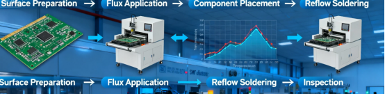
Soldering is at the heart of the PCB assembly process, forming the electrical and mechanical connections between components and the board. The soldering process typically involves heating solder—often in the form of solder paste for SMT or solder wire for through-hole components—using a soldering iron or reflow oven. Flux is applied to remove oxides from the copper pads and component leads, ensuring that the solder wets the surfaces properly and forms strong, reliable joints. Solder wick is an essential tool for removing excess solder from the PCB surface, especially during rework or when correcting solder bridges.
Different assembly processes require tailored soldering techniques. Through-hole components, such as electrolytic capacitors and connectors, are soldered by inserting their leads into plated holes and applying heat and solder from the opposite side. SMT components, including resistors, diodes, and ICs, are placed directly onto tinned pads and soldered using reflow or selective soldering. Each component type presents its own challenges—electrolytic capacitors must be oriented correctly to avoid polarity issues, while diodes and transistors require careful heat management to prevent damage.
Beyond soldering, the assembly process includes precise component placement, thorough inspection, and rigorous testing to ensure product quality. Selective soldering is often used for complex boards with mixed technology, allowing specific components or areas to be soldered without affecting the rest of the assembly. Hot air soldering is particularly useful for BGA components, where uniform heating is crucial for reliable connections. Throughout the process, improper handling and mechanical stress can damage copper pads and component leads, underscoring the importance of robust quality assurance protocols.
The electronics industry is continually evolving, with a growing emphasis on environmental responsibility and product quality. Lead-free soldering has become the standard in many regions, driven by regulatory requirements and consumer demand. Organic solderability preservative (OSP) coatings are increasingly used to enhance solderability and extend the shelf life of PCBs, while minimizing environmental impact.
In this context, pad add tinning plays a vital role in maintaining the solderability and reliability of printed circuit boards. Over time, even the best surface finishes can degrade, especially if PCBs are stored for extended periods. Tinning—applying a thin layer of tin or other solderable material to copper pads and component leads—prevents oxidation and ensures that solder will flow smoothly during assembly. By using tinned surfaces, PCB manufacturers can guarantee strong, consistent solder joints, whether assembling through-hole or SMT components. This attention to detail in the tinning process is crucial for delivering high-quality, reliable electronic devices that meet the demands of today’s market.
Key Application Scenarios of Line/Pad Add Tinning
Line/pad add tinning is not a one-size-fits-all process—it shines in specific scenarios where its targeted reinforcement and repair capabilities are most needed. Below are the most common application areas:
High-Reliability Electronic Products
Industries such as aerospace, medical devices, and automotive electronics have zero tolerance for PCB failures. For example, PCBs used in cardiac pacemakers must operate stably for years, while those in aircraft control systems must withstand extreme temperature changes and vibrations. In these cases, line/pad add tinning is applied to critical lines and pads (such as power supply traces and sensor connections) to enhance corrosion resistance and connection reliability, reducing the risk of sudden failures.
Long-Term Storage or Stocked PCBs
Many manufacturers maintain stockpiles of standard PCBs to meet urgent orders. However, prolonged storage can degrade the solderability of copper surfaces. Before assembling these stocked PCBs, adding a fresh tin layer revitalizes the lines and pads, ensuring they perform as well as newly fabricated boards. This is a common practice in the consumer electronics industry, where product launches often require quick assembly of pre-stored PCBs.
Repairs and Modifications of Prototype PCBs
During the R&D phase, engineers frequently modify prototype PCBs to test new designs or fix bugs. These modifications may involve cutting existing lines, adding new pads, or reworking solder joints. For example, replacing or troubleshooting a resistor is a common task during such modifications, requiring careful removal and resoldering to ensure proper circuit function. Add tinning is essential for these tasks—it helps repair damaged copper traces, improve the solderability of modified areas, and ensure that the prototype performs consistently with the design specifications. For startups and R&D labs, this process saves time and costs compared to fabricating new prototypes for every modification.
High-Current or High-Temperature PCBs
PCBs used in power electronics—such as inverters, power supplies, and LED drivers—handle high currents that generate significant heat. Over time, this heat can cause solder joints to degrade and copper lines to oxidize. Adding tin to high-current lines and power pads enhances heat dissipation (tin has good thermal conductivity) and prevents oxidation, extending the lifespan of the PCB. For example, LED street light PCBs often undergo add tinning on their power traces to ensure stable operation under long-term high-temperature conditions.
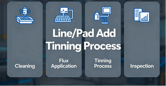
How to Perform Line/Pad Add Tinning Correctly
The effectiveness of line/pad add tinning depends largely on proper operation. Improper techniques can lead to issues like uneven tin layers, tin bridging, or damage to the PCB. Below is a step-by-step guide to the standard process, along with key considerations.
Preparation Work:
Before starting, ensure you have all necessary tools: soldering iron, solder wire, flux, tweezers, and cleaning materials. Use a static-proof tray to organize and handle electronic components during the tinning process, which helps protect sensitive semiconductors from static discharge.
Preparation Work
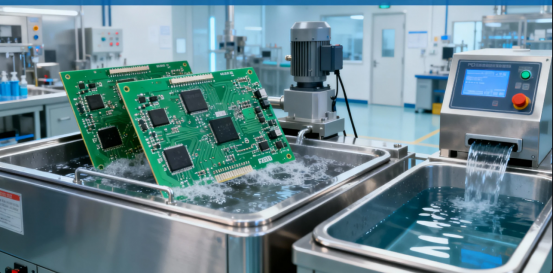
·PCB Cleaning: Before adding tin, the PCB must be thoroughly cleaned to remove dirt, grease, and oxide layers. Use isopropyl alcohol or a specialized PCB cleaning agent, and dry the board completely with compressed air or a lint-free cloth. Contaminants on the surface will prevent the tin layer from adhering properly, resulting in poor bonding.
·Tool Preparation: The tools needed vary based on the scale of operation. For small-batch or prototype work, hand tools like soldering irons (with a fine tip for precision), solder wire (preferably lead-free tin-silver-copper alloy, which complies with environmental standards), and flux are sufficient. For mass production, automated equipment such as selective soldering machines or laser tinning systems is used to ensure consistency.
·Parameter Confirmation: Determine the thickness of the tin layer based on the application. For general-purpose PCBs, a 1–2 micron layer is sufficient; for high-reliability products, increase it to 2–3 microns. Additionally, set the soldering temperature appropriately—too high a temperature can damage the PCB substrate, while too low a temperature will result in incomplete tin melting.
Core Operation Steps
·Apply Flux: Apply a small amount of flux to the target lines or pads. Flux removes surface oxides, improves solder wetting, and prevents re-oxidation during soldering. For fine-pitch pads, use a flux pen for precise application to avoid contaminating adjacent areas.
·Tin Application: For manual operation, heat the soldering iron to the recommended temperature (typically 350–380°C for lead-free solder), touch the solder wire to the tip to form a small solder bead, then gently glide the tip along the line or over the pad. Control the speed and pressure to ensure an even tin layer—avoid piling up tin, which can cause bridging. For automated production, laser tinning systems use focused laser beams to melt solder, depositing a uniform layer on targeted areas with high precision.
·Post-Tinning Cleaning: After the tin layer cools and solidifies, clean the PCB again to remove residual flux. Flux residue can corrode the PCB over time, especially in humid environments. Use a flux remover and dry the board thoroughly.
·Quality Inspection: Check the tinned lines and pads with a magnifying glass or microscope. Ensure the tin layer is uniform, free of bubbles, cracks, or bridging. Test the solderability by soldering a sample component to verify that the solder flows smoothly and forms a strong joint.
Key Precautions
·Avoid overheating the PCB: Prolonged exposure to high temperatures can warp the substrate or damage nearby components. Work quickly and focus the heat on the target area.
·Use the right solder type: Lead-free solder is mandatory for most consumer electronics due to environmental regulations. For high-temperature applications, choose a tin-silver alloy with a higher melting point.
·Maintain tool cleanliness: A dirty soldering iron tip can cause poor heat transfer and uneven tinning. Clean the tip regularly with a brass wire sponge during operation.
Common Problems in Line/Pad Add Tinning and Their Solutions
Even with careful operation, issues can arise during line/pad add tinning. Below are the most frequent problems, their root causes, and actionable solutions to resolve them.
Uneven Tin Layer
Symptom: The tin layer on lines or pads is thick in some areas and thin in others, or there are gaps in the layer.Causes: Uneven application of flux, inconsistent temperature of the soldering iron, or uneven movement speed during manual operation. For automated systems, this may be due to misalignment of the tinning head or inconsistent solder supply.Solutions: Ensure uniform flux application; calibrate the soldering iron temperature regularly and maintain a steady speed while tinning. For automated equipment, check and adjust the alignment of the tinning head, and inspect the solder supply system for blockages.
Tin Bridging
Symptom: Tin connects adjacent lines or pads, creating unintended electrical connections.Causes: Excessive solder usage, inaccurate targeting of the soldering tool, or insufficient spacing between fine-pitch pads.Solutions: Reduce the amount of solder used; use a finer soldering iron tip for precision work. For fine-pitch designs, use laser tinning for better control. If bridging occurs, use a desoldering wick to absorb excess tin and repair the affected area.
Poor Adhesion of Tin Layer
Symptom: The tin layer peels off easily when touched or during component soldering.Causes: Incomplete cleaning of the PCB surface, residual contaminants, or oxidation of the copper substrate before tinning.Solutions: Re-clean the PCB with a more effective cleaning agent, ensuring all oxides and contaminants are removed. If the copper surface is severely oxidized, lightly polish it with fine sandpaper before cleaning and tinning.
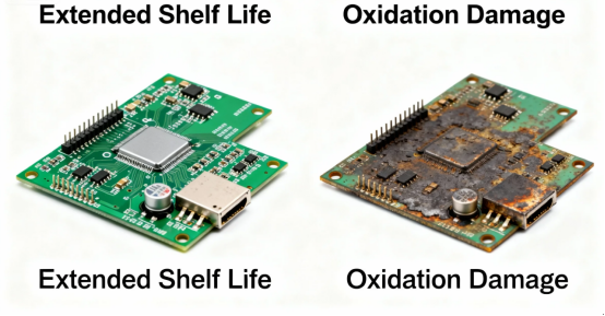
Oxidation of Tinned Surface
Symptom: The tinned surface turns dull or discolored shortly after processing.Causes: Exposure to air for extended periods after tinning, or use of low-quality tin with impurities.Solutions: Complete the component assembly as soon as possible after tinning. For PCBs that need to be stored, package them in anti-static bags with desiccant. Use high-purity tin solder to reduce the risk of rapid oxidation.
Future Trends of Line/Pad Add Tinning

As PCB technology advances, line/pad add tinning is also evolving to meet new challenges and demands. Here are two key trends shaping its future:
Environmentally friendly tin alloys: With increasing environmental regulations, manufacturers are shifting towards lead-free solder alloys made from tin, silver, and copper. These new materials present fewer environmental and health concerns compared to traditional leaded solders.
Automation and Precision Enhancement
With the widespread adoption of high-density, miniaturized PCBs, manual tinning can no longer meet the requirements for precision and consistency. Automated solutions such as laser tinning and selective soldering are becoming increasingly popular. Laser tinning, in particular, offers unparalleled precision—its focused beam can target areas as small as a few microns, making it ideal for micro-pads and ultra-narrow lines. These automated systems also integrate quality inspection modules, using machine vision to detect defects in real time and adjust parameters, further improving production efficiency and quality.
Development of Environmentally Friendly and High-Performance Tin Alloys
As global environmental regulations become stricter, the shift from leaded to lead-free tin is irreversible. Researchers are developing new tin-based alloys to address the shortcomings of existing lead-free solder, such as higher melting points and lower ductility. For example, tin-silver-copper alloys with trace amounts of nickel or bismuth have been shown to improve solder joint reliability and reduce brittleness. Additionally, environmentally friendly fluxes that are free of halogens and volatile organic compounds (VOCs) are being paired with these alloys, making line/pad add tinning more sustainable.
Conclusion
Line/pad add tinning may be a small step in PCB assembly, but its impact on product quality and reliability is profound. By preventing oxidation, strengthening connections, repairing defects, and adapting to miniaturized designs, this process helps manufacturers avoid costly reworks, reduce scrap rates, and deliver more durable electronic products.
Whether you’re a seasoned manufacturer or a novice in PCB assembly, mastering the principles, techniques, and best practices of line/pad add tinning is a worthwhile investment. As technology advances, embracing automated tools and eco-friendly materials will further enhance the value of this process, supporting the development of next-generation electronics.
The next time you encounter soldering defects or reliability issues in PCB assembly, consider whether line/pad add tinning could be the solution. With the right approach, this simple yet powerful process can turn potential failures into successful, long-lasting products.
FAQs
Q: What is line/pad add tinning in PCB assembly?
A: It refers to the process of applying a 1-3 micron layer of tin or tin-based alloy onto the conductive traces and component solder pads of a PCB during the assembly stage. This addresses specific assembly issues and enhances performance.
Q: If there is an initial surface finish, why is additional tinning necessary?
A: It specifically prevents copper oxidation, strengthens the mechanical and electrical properties of solder joints, repairs minor manufacturing defects, and accommodates the soldering requirements of high-density, miniaturized PCBs, thereby improving yield.
Q: In which scenarios is line/pad add tinning essential?
A: Critical applications include high-reliability products (aerospace, medical, automotive electronics), PCBs in long-term storage, prototype modifications during R&D, and power electronics PCBs operating under high-current or high-temperature conditions.
Q: What are the core steps for manual add tinning?
A: First, clean the PCB to remove contaminants and apply flux. Heat the soldering iron to 350-380°C (for lead-free solder) and apply tin precisely. After cooling, clean off any residual flux and finally inspect the quality of the tin layer.
Q: How should solder bridges be addressed after tinning?
A: Use a desoldering wick to remove excess solder. Subsequently, reduce the amount of solder used, switch to a finer soldering iron tip, and for fine-pitch pads, prioritize laser tinning to achieve higher precision.
Q: What causes poor adhesion of the tin layer?
A: This is often due to insufficient cleaning of the PCB surface, leaving contaminants, or oxidation of the copper substrate before tinning. Inadequate preparation before application results in poor adhesion.
Q: What are the future development trends for add tinning processes?
A: Firstly, automation upgrades (e.g., laser tinning) improve precision and consistency. Secondly, developing environmentally friendly, high-performance tin alloys and halogen-free fluxes aligns with environmental regulations.
Q: How is the thickness of the tin layer selected for add tinning?
A: For standard PCBs, 1-2 microns is sufficient. For products requiring higher reliability, the thickness can be increased to 2-3 microns.
Author: Jack Wang

