


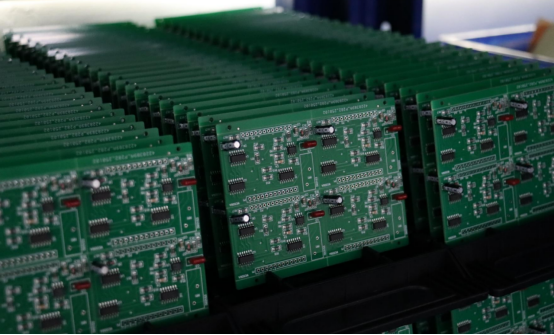
Printed Circuit Board Rework Explained: How to Fix PCBs Efficiently
Even the most carefully manufactured printed circuit boards can run into problems. A tiny solder joint issue, a misaligned component, or a subtle connection failure can cause a device to malfunction or underperform. Being able to address these issues efficiently not only saves time and costs but also ensures the board continues to operate reliably. Skilled PCB rework turns what might seem like a lost board into a fully functional component, making precision and proper technique essential for any electronics professional.
Introduction to Printed Circuit Board (PCB) Rework
What is PCB Rework?
PCB rework is the process of correcting or modifying a printed circuit board after it has been manufactured. Its main purpose is to fix defects, replace faulty components, or make small adjustments without having to produce a new board. Essentially, rework ensures that the board meets functional and quality standards.
It is important to distinguish PCB rework from other related activities:
PCB Repair: Typically used for fixing severe or permanent damage, such as broken traces or burned components, where rework alone may not be sufficient.
Prototyping Adjustments: Small design changes made during the development phase, often before mass production. Unlike rework, these are planned modifications rather than corrections.
Common examples of PCB rework include:
Repairing a cold or bridged solder joint that causes intermittent connectivity.
Replacing a damaged resistor, capacitor, or integrated circuit.
Adjusting component placement to improve signal integrity or thermal performance.
These tasks often require precision tools, steady hands, and careful inspection to avoid causing further damage.
Importance of Efficient PCB Rework
Efficient PCB rework is critical for both cost-effectiveness and product reliability.
1. Reducing Costs: Reworking a board is usually far less expensive than manufacturing a replacement. For complex or multilayer PCBs, a single rework can save significant production costs.
2. Minimizing Production Downtime: Quick and accurate rework allows products to stay on schedule. Delays caused by board failures can disrupt assembly lines and affect delivery timelines.
3. Maintaining Product Reliability and Quality: Properly executed rework ensures that the repaired board functions as intended. This helps maintain high standards for product performance and reduces the risk of future failures.
For example, a team that replaces a faulty surface-mounted IC on a multilayer PCB can restore full functionality without affecting other components. By contrast, improper rework could introduce shorts or lift pads, resulting in a board that performs worse than before.
In summary, PCB rework is a targeted, precise process that corrects defects and preserves both time and resources. Its proper application ensures that electronic devices meet quality expectations while minimizing waste and operational disruption.
Common Causes for PCB Rework
Manufacturing Defects
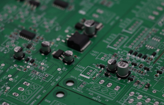
Manufacturing defects are one of the most frequent reasons for PCB rework. These defects occur during the assembly process and can affect the board’s performance or functionality. Common examples include:
Solder bridging: This happens when excess solder creates an unintended connection between two or more adjacent pins, causing short circuits.
Cold joints: Cold solder joints occur when solder does not properly melt or bond to the component or pad, resulting in weak or intermittent electrical connections.
Misaligned components: Components may be placed slightly off their designated positions, which can affect connectivity or mechanical stability.
These defects often arise due to improper soldering temperatures, inaccurate pick-and-place machinery, or inconsistent flux application. For instance, a surface-mounted resistor misaligned by just 0.2 mm can lead to a poor connection that requires rework before the board can function reliably.
Component Failures
Component failures are another major cause of PCB rework. Individual parts on the board may fail due to manufacturing flaws, handling errors, or environmental stress. Typical component failures include:
Dead ICs: Integrated circuits that no longer operate correctly.
Damaged capacitors or resistors: Components that are cracked, overheated, or otherwise compromised.
Faulty connectors: Loose or broken connectors that disrupt signal or power transmission.
Failing components can be identified through visual inspection or functional testing. Visual signs include burn marks, cracked packages, or bent leads. Functional tests may involve using a multimeter, oscilloscope, or in-circuit tester to check voltage, current, or signal continuity. For example, a faulty capacitor may show normal appearance but fail under testing, necessitating replacement during rework.
Design or Layout Errors
Sometimes the need for PCB rework originates from the design phase rather than manufacturing. Design or layout errors can require post-production modifications to ensure the board functions as intended. Examples include:
Incorrect trace routing that causes signal interference or impedance mismatch.
Component placement that obstructs cooling or assembly.
Missing vias or pads that prevent proper connectivity.
Design fixes often involve adjusting the PCB layout in CAD software before mass production. In contrast, on-board rework addresses these errors after the board is already manufactured. For instance, a trace reroute on a multilayer board may be added using wire jumpers or solder bridges, while software-based design corrections prevent future boards from requiring the same rework.
Tools and Equipment for PCB Rework
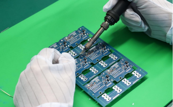
Soldering and Desoldering Tools
Soldering and desoldering tools are essential for performing precise PCB rework. Common tools include:
Soldering Irons: Available in temperature-controlled and fixed-temperature models. They are used for manually soldering components onto the PCB.
Hot Air Rework Stations: Provide controlled heat for soldering or desoldering surface-mounted components, especially for ICs and BGAs.
Solder Wick: A braided copper wire used to remove excess solder from joints.
Desoldering Pumps: Vacuum tools that remove molten solder efficiently from through-hole pads.
Step-by-step guidance for tool usage:
1. Heat the solder joint using a soldering iron or hot air station.
2. Use a solder wick to absorb excess solder, or a desoldering pump to remove it quickly.
3. Ensure the pad or component lead is clean before placing a replacement component.
4. Apply flux to improve solder flow and create a reliable joint.
Proper selection and handling of these tools prevent board damage and ensure high-quality rework results.
Inspection and Testing Equipment
Accurate inspection and testing are critical to identifying defects before and after rework. Key equipment includes:
Multimeters: Measure voltage, current, and resistance to detect electrical issues.
Microscopes: Magnify solder joints and components to reveal cracks, cold joints, or misalignments.
Thermal Cameras: Identify hotspots that indicate component or trace issues.
Oscilloscopes: Analyze signal integrity and waveform issues on high-speed circuits.
Example of fault detection: A technician may use a microscope to spot a hairline crack in a capacitor’s solder joint, then confirm functionality with a multimeter. Thermal cameras can reveal overheating ICs that may require rework. Using these tools together ensures efficient diagnosis and reduces the risk of missed defects.
Safety and ESD Precautions
Electrostatic discharge (ESD) can irreversibly damage sensitive components during rework. Following proper safety and ESD precautions is essential:
ESD Mats and Wrist Straps: Ground the technician and the workspace to prevent static buildup.
Anti-Static Measures: Use anti-static bags, conductive trays, and humidity control to minimize electrostatic risk.
Best Practices: Avoid touching component leads directly, maintain a clean workspace, and ensure proper grounding for all tools.
Following these precautions reduces the risk of component failure and ensures that rework is performed safely and reliably.
Step-by-Step PCB Rework Process
Preparation and Planning
Effective PCB rework begins with careful preparation and planning. Start by inspecting the board to identify faulty components, solder joints, or any visible defects. Visual inspection with a magnifying lens or microscope helps detect issues like cold solder joints, lifted pads, or misaligned parts.
Next, document the existing soldering points and layout. This includes noting component positions, orientation, and trace paths. Maintaining accurate documentation ensures that rework does not introduce new errors and allows for easier verification after repair. For complex multilayer boards, creating a schematic or annotated diagram can guide the rework process.
Component Removal
Removing defective components safely is a critical step in PCB rework. Common techniques include:
Hot Air Rework: Used for surface-mounted components, particularly ICs, QFPs, and BGAs. Hot air evenly heats the solder until the component can be lifted without damaging the board.
Soldering Iron: Suitable for through-hole components or smaller surface-mounted parts. Apply heat to each lead and use a desoldering pump or solder wick to remove solder.
Examples:
Removing a QFP requires heating all pins evenly with hot air to avoid bending or lifting leads.
A BGA may require preheating and careful reflow to prevent thermal stress.
Through-hole resistors or connectors can often be removed with a soldering iron and pump without affecting adjacent traces.
Board Cleaning and Inspection
After component removal, the board must be thoroughly cleaned. Use flux remover, isopropyl alcohol, and soft brushes to eliminate solder residues, flux buildup, and contaminants.
Next, inspect the board for pad damage or lifted traces. Damaged pads can be repaired with wire bridges or copper tape if necessary. Ensuring the board surface is clean and intact prevents poor solder joints and ensures proper electrical connectivity during component replacement.
Component Replacement and Soldering
Reinstalling components correctly is essential for reliable operation. Steps include:
1. Apply flux to the pads to improve solder flow and adhesion.
2. Place the replacement component accurately according to documented orientation and layout.
3. Solder the component using either manual soldering or reflow techniques.
Examples and considerations:
Leaded solder is easier to work with and has a lower melting point, making it suitable for manual soldering.
Lead-free solder requires higher temperatures and careful thermal control to avoid pad damage, especially on multilayer boards.
Following proper reflow profiles for each type of solder ensures strong, reliable joints.
Post-Rework Testing
Once rework is complete, the board must be thoroughly tested to confirm functionality.
Functional Testing: Power on the board and check voltage, current, and signal flow at critical points.
Automated Testing or In-Circuit Testing (ICT): Use tools to verify connectivity, component function, and signal integrity efficiently.
For example, after replacing a surface-mounted IC, use a multimeter and oscilloscope to ensure the signals at each pin match expected values. Post-rework testing confirms that the board performs as intended and reduces the risk of latent failures.
Best Practices and Efficiency Tips
Time-Saving Techniques
Efficient PCB rework saves both time and resources. One effective strategy is preheating the boards before component removal or soldering. Preheating reduces thermal stress and allows solder to flow more easily, making desoldering and reflow faster.
Batch rework strategies are another time-saver. Performing similar repairs on multiple boards simultaneously can improve workflow efficiency, especially in production environments.
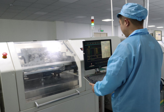
When comparing manual vs. automated rework processes:
Manual rework offers flexibility for small-scale or delicate repairs but can be slower and more prone to human error.
Automated rework stations provide consistent heat profiles and placement accuracy, making them ideal for repetitive or high-volume tasks. Combining manual and automated techniques often provides the best balance of speed and precision.
Avoiding Common Mistakes
Even experienced technicians can make mistakes during PCB rework. Common issues include:
Overheating pads, which can lift traces or damage layers.
Solder bridging, where excess solder connects unintended pins.
Improper flux application, leading to weak joints or oxidation.
Corrective actions for these mistakes include:
Using solder wick or a desoldering pump to remove bridges.
Reapplying flux and reheating carefully to form a proper joint.
Repairing lifted pads with copper tape or wire jumpers if necessary.
Being aware of these pitfalls and addressing them promptly ensures reliable repairs and reduces the risk of repeat rework.
Documentation and Continuous Improvement
Maintaining detailed rework logs is essential for quality assurance and process optimization. Logs should record the type of defect, tools used, steps taken, and outcome of the rework. This data helps identify recurring issues and track efficiency over time.
Using feedback from these records enables teams to reduce recurring defects. For example, if multiple boards show cold solder joints in the same area, adjusting soldering temperature or improving flux application in future batches can prevent the issue from repeating.
Continuous monitoring and documentation foster both higher quality and faster, more predictable PCB rework processes.
Advanced PCB Rework Scenarios
High-Density and Multi-Layer Boards
Reworking high-density and multi-layer PCBs presents unique challenges. Fine-pitch components have very small lead spacing, making soldering and desoldering more difficult. Microvias—tiny holes connecting layers—are fragile and can easily lift or short if overheated.
Layer-sensitive rework techniques include:
Using precise temperature-controlled hot air stations to avoid overheating inner layers.
Applying localized heat only to the affected area to protect nearby traces.
Employing microscopic inspection during and after rework to ensure microvias and fine-pitch joints are intact.
For example, a 0.4 mm pitch IC requires careful alignment and controlled soldering to prevent bridging or damage to surrounding pads.
BGA (Ball Grid Array) Rework
BGA components require specialized procedures due to their hidden solder joints beneath the package. The step-by-step BGA rework process includes:
1. Preheating the PCB to reduce thermal shock.
2. Using a hot air rework station with precise temperature control to soften the solder balls.
3. Removing the BGA carefully without lifting pads.
4. Cleaning old solder from the pads using solder wick or flux.
5. Placing the new BGA with accurate alignment tools.
6. Reflowing solder balls following the correct thermal profile.
Example: Thermal profiling ensures each solder ball melts and solidifies uniformly. If solder balls are damaged or uneven, replacing them individually may be necessary to maintain reliable connectivity.
Rework in High-Frequency or High-Speed PCBs
Reworking high-frequency or high-speed PCBs requires attention to signal integrity. Even small variations in trace geometry or impedance can affect performance.
Key considerations and techniques:
Maintain consistent trace impedance when adding jumpers or repairing traces.
Use low-inductance soldering techniques to minimize signal disruption.
Employ specialized RF inspection tools, such as network analyzers or high-speed oscilloscopes, to verify performance after rework.
For example, repairing a microstrip trace on an RF board requires maintaining the same width and dielectric spacing; otherwise, signal reflections may degrade communication performance.
Conclusion
Efficient PCB rework combines careful planning, the right tools, and precise techniques to restore board functionality while saving time and cost. By following step-by-step processes—from inspection and component removal to soldering and post-rework testing—technicians can achieve reliable results on everything from simple single-layer boards to complex multilayer and high-speed PCBs. Using proper safety measures, maintaining detailed documentation, and learning from past repairs further enhance efficiency and quality. Looking ahead, technologies like automation, AI-assisted inspection, and predictive maintenance are set to transform PCB rework, reducing human error and increasing production throughput. Companies like PCBMASTER are leading the way by integrating these innovations into their high-performance PCB solutions, helping clients achieve longer product lifespans and consistent board reliability.
FAQs
What is the difference between PCB rework and PCB repair?
PCB rework focuses on correcting minor defects or making adjustments to components after the board has been manufactured, such as fixing a cold solder joint or replacing a faulty IC. PCB repair, on the other hand, deals with more serious damage, like broken traces, burned components, or structural board failures. Rework is usually less invasive and aims to restore functionality without replacing the entire board, while repair often requires more extensive fixes.
How can I prevent damaging the PCB during rework?
Preventing damage starts with proper preparation and handling. Use temperature-controlled soldering tools, apply heat only to the affected area, and avoid excessive pressure on pads or traces. Implement ESD precautions, such as wrist straps and anti-static mats, and inspect the board carefully before and after rework. Maintaining steady hands and following precise step-by-step procedures reduces the risk of lifted pads, trace damage, or component failure.
Which tools are essential for small vs. large-scale PCB rework?
For small-scale or precision rework, essential tools include a fine-tip soldering iron, hot air station, solder wick, and magnification equipment like a microscope. For large-scale or high-volume rework, automated rework stations, batch preheating ovens, pick-and-place machines, and in-circuit testers are more effective. Combining manual and automated tools often provides flexibility and efficiency depending on board complexity.
Can PCB rework be automated, and if so, how?
Yes, PCB rework can be partially or fully automated. Automated systems use precise heat control, vision-assisted alignment, and robotic soldering or component placement to perform repetitive or complex tasks. For example, automated BGA rework stations can remove, clean, and reflow components with minimal human intervention, improving consistency and reducing errors in high-volume production.
How do I test a PCB after rework to ensure full functionality?
Testing begins with visual inspection to check solder joints and component placement. Functional testing includes powering the board and measuring voltages, currents, and signals at key points. For more thorough verification, in-circuit testing (ICT), automated test equipment, or oscilloscopes can be used to confirm connectivity and signal integrity. Proper post-rework testing ensures that all components operate correctly and the board performs as intended.

