


Choosing Between PCB Assembly Single Side and Both Side for Your Needs
Introduction
In the field of electronic device manufacturing, PCB assembly is a critical process that significantly impacts product performance and cost.
When we open up almost any electronic device, we can find a printed circuit board (PCB) populated with various components. These green or black boards carry the "lifeline" of electronic products. But did you know these circuit boards are primarily assembled using either single-side or double-side methods? Each approach has its unique advantages and suitable application scenarios.
This article will provide an in-depth understanding of the differences between single-side and double-side PCB assembly, helping you make more informed decisions in your product designs.
PCB Assembly Basics: What Are Single-Side and Double-Side Assembly?
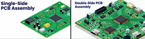
Printed circuit boards are categorized into single-sided boards, double-sided boards, and multi-layer boards based on the number of conductive layers. Each pcb type—single-sided, double-sided, and multi-layer PCBs—has distinct structural features and is suited for different levels of design complexity and application requirements.
Single-sided boards use an insulating substrate with a single conductive layer of copper foil on only one side, serving as the main conductive material. The conductive pattern, including solder pads for securing and connecting component leads and printed traces for interconnecting component pins, can only be created on this copper-clad surface. This conductive pattern side is called the solder side or bottom layer, while the side without copper is used for placing components and is called the component side or top layer. Single layer boards are a type of single-sided printed circuit, or sided printed circuit, characterized by their straightforward structure.
Single-sided boards have a simple structure and low production costs, requiring less material due to their single layer design. However, they present the greatest challenges in routing design, with lower routing completion rates. A few nodes that cannot be connected by printed traces must be connected using jumper wires. When design complexity increases beyond what single-sided boards can handle, engineers often turn to multi layer pcbs as an alternative solution.
Double-sided boards have an insulating substrate covered with copper foil on both top and bottom surfaces, allowing component pads and printed traces to be fabricated on both sides. In double-sided boards, components can be mounted on the top layer, while the other side serves as the bottom solder layer, with plated through-holes achieving electrical interconnection between the two sides. Double-sided boards have higher production costs but relatively easier routing design and higher routing completion rates.
Differences in Production Processes
Single-Sided Board Production Process
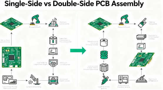
The production process for single-sided boards is relatively straightforward: CAD or CAM → CCL cutting, drilling of tooling holes → printing conductive pattern, curing → etching, resist removal, cleaning → printing solder mask pattern, curing → printing marker characters, curing → drilling and punching tooling holes, blanking → circuit inspection, testing → coating of solder mask or OSP → inspection, packaging, finished product.
Due to their simple production process and fewer required steps, single-sided boards have lower production costs and relatively shorter production cycles.
Double-Sided Board Production Process
The production process for double-sided boards is more complex: CAD and CAM → CCL cutting/edge grinding → NC drilling → hole metallization (pattern plating or panel plating) → dry film or wet film method (negative pattern) or mask/plugging (positive pattern) → copper/tin-lead plating or pattern transfer → resist removal, etching → tin-lead stripping, contact finger plating → printing solder mask/characters → hot air leveling or OSP → milling/punching outline → inspection/testing → packaging/finished product.
The core feature of double-sided boards is the presence of plated through-holes that connect the circuits on both layers, a process that requires additional chemical treatment and plating steps.
Differences in SMT Assembly Processes
Surface Mount Technology (SMT) is currently the most popular technology and process in the electronic assembly industry. Double sided assembly refers to the process of mounting electronic components on both sides of a PCB, which is especially useful for complex or high-performance designs.
Depending on the electronic components used and product requirements, the soldering configuration of components on PCBs is mainly divided into single sided SMT assembly, double sided SMT assembly, single-side mixed assembly, and double-side mixed assembly. In single sided SMT assembly, components are mounted only on one side of the PCB, while double sided SMT assembly involves placing components on both sides, requiring additional steps such as flipping the PCB and using a reflow oven during the reflow soldering process.
Single-Side SMT Assembly
Single-side full SMT refers to all surface mount components being placed on one side of the PCB. The process flow for this assembly method is simple: solder paste printing → component placement → reflow soldering. Single-side assembly is suitable for electronic products with fewer components and relatively simple circuits, such as simple control modules and basic home appliance circuits.
Single-side mixed assembly means both through-hole and surface mount components are on the same side of the PCB. This assembly method requires combining both reflow and wave soldering processes: first reflow soldering for surface mount components, followed by wave soldering for through-hole components.
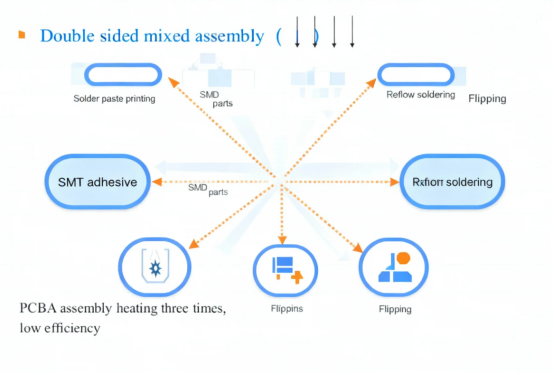
Double-Side SMT Assembly
Double-side full SMT means surface mount components are placed on both sides A and B of the PCB. This layout approach ensures the aesthetic appeal and functionality of the PCB board while fully utilizing PCB space to achieve minimal PCB area. Double-sided SMT assembly is particularly suitable for complex designs that require advanced routing and higher component density.
The assembly process for double-side full SMT is as follows:
·Bottom side: solder paste printing → component placement → reflow soldering
·Top side: solder paste printing → component placement → reflow soldering
The reason for soldering the bottom side first is that the SMDs laid out on the bottom side are generally selected considering the requirement that they should not fall off during soldering.
Double-side mixed assembly involves both through-hole and surface mount components on both sides of the PCB. This assembly method is more complex and requires selecting different soldering processes based on specific circumstances, such as masked selective wave soldering or movable nozzle selective wave soldering.
Component Placement Considerations
When designing a printed circuit board, component placement is a crucial factor that can significantly influence the performance and manufacturability of your product. With single sided PCBs, all components are mounted on one side of the board, which simplifies assembly and reduces the risk of certain manufacturing defects. However, this approach also limits the complexity of the circuit design, as there is only one side available for routing copper traces and placing components. This can restrict component density and make it challenging to implement more complex circuits, especially when space is limited.
In contrast, double sided PCBs provide much greater flexibility in component placement. By utilizing both the top and bottom layers of the circuit board, designers can achieve higher component density and accommodate more complex circuit designs. This is particularly beneficial for applications that require advanced functionality or compact layouts. However, the increased complexity of double sided PCBs also introduces new challenges, such as the potential for misaligned vias and other manufacturing defects that can impact signal integrity and overall device reliability.
To optimize component placement, it’s important to consider factors like heat dissipation, copper thickness, and the specific requirements of your circuit design. Proper planning can help ensure that components are positioned to minimize thermal buildup, maintain signal integrity, and support efficient manufacturing. Whether you’re working with single sided or double sided PCBs, thoughtful component placement is key to achieving a reliable and high-performing final product.
Single-Side or Double-Side Assembly? Key Considerations
1. Cost and Complexity
Single-sided boards have a simple structure and low production costs, but they present the greatest challenges in routing design with low routing completion rates. Double-sided boards have higher production costs but relatively easier routing design and higher routing completion rates.
If your circuit design is relatively simple, doesn't require high-density routing, and is cost-sensitive, single-side assembly may be the more economical choice.
2. Space Constraints
The biggest advantage of double-side assembly is the ability to fully utilize PCB space to achieve minimal board area. For portable devices, smartphones, wearable devices, and other products with strict space limitations, double-side assembly is almost an inevitable choice.
3. Circuit Performance Requirements
High-frequency circuits or interference-sensitive designs may need to consider using double-sided boards. In double-sided circuit boards, to prevent radiation generated by high-frequency clock signals, a grounded metal-filled area can be placed in the bottom layer below the clock circuit, avoiding trace routing underneath the clock circuit. Such shielding measures are difficult to implement on single-sided boards.
4. Thermal Management
Designs with high power density may need to utilize both sides of the PCB to distribute thermal load. Double-sided boards can more effectively dissipate heat by transferring it from one layer to another through vias. For some high-power applications, even if the circuit itself doesn't require double-side routing, double-sided boards might still be chosen for thermal management considerations.
5. Production Yield and Reliability
For double-side assembled PCBA, the flatness of the second soldered side is inferior to that of the first soldered side. PCBs are laminated products of different materials with internal stress, and they warp after the first soldering process.
This warpage affects the solder paste printing on the second soldering side. For components sensitive to solder paste volume (such as dual-row QFN, 0.4mm QFP, etc.), the impact of warpage on solder paste thickness or volume must be considered during layout.
Design Considerations and Best Practices
Regardless of whether you choose single-side or double-side assembly, the following design considerations can help optimize PCB performance and production efficiency:
·Component Placement: First manually place core components, power and signal connectors, interference-sensitive components, and high-power components, then automatically place the remaining components, and finally manually adjust the positions of individual components.
·Zoned Placement: In circuit systems, digital circuits, analog circuits, and high-current circuits must be placed in separate zones, making it easier for the reference ground lines of each area to implement single-point grounding.
·Decoupling Capacitor Arrangement: In principle, connect a decoupling capacitor between the power and ground pins of every 1-4 digital IC chips.
·Printed Trace Design: Choose 135° for inner corners at printed trace turning points, avoiding turns less than 90°. For low-voltage circuits, the minimum spacing can be 10 mil.
PCB Design for Manufacturability
Designing a PCB with manufacturability in mind is essential for ensuring a smooth production process and a high-quality final product. For single sided PCBs, the design process is generally more straightforward, as there are fewer components and only one conductive layer to manage. This simplicity can help reduce the risk of manufacturing defects and streamline assembly, making single sided PCBs a cost-effective choice for less complex applications.
Double sided PCBs, on the other hand, require more careful consideration during the design phase. With components placed on both the top and bottom layers, designers must plan conductive paths to avoid interference and maintain signal integrity. The increased component density and the need to manage multiple layers add complexity to the design process, making it even more important to collaborate with an experienced manufacturing partner.
Working closely with your manufacturing partner can help you make informed decisions about surface finishes, such as electroless nickel immersion gold (ENIG), which can enhance solderability and protect copper traces. By addressing manufacturability early in the design process—considering factors like component density, layer count, and the type of PCB—you can minimize the risk of manufacturing defects and ensure that your printed circuit board meets both performance and quality standards.
Double Sided PCB Applications
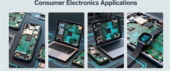
Double sided PCBs are the backbone of many modern electronic devices that demand advanced functionality and compact design. Their ability to support higher component density and more complex circuits makes them ideal for a wide range of applications, from consumer electronics like smartphones and remote controls to industrial equipment and sophisticated medical devices. In these environments, double sided PCBs enable complex routing and the integration of high-speed signals, which are essential for devices that require fast data processing and reliable performance.
The use of both sides of the board allows for more efficient use of space, making double sided PCBs a cost effective solution for products where size and weight are critical factors. Applications such as LED lighting, telecommunications equipment, and high-speed data processing systems benefit from the improved signal integrity and impedance control that double sided PCBs provide. Whether you’re designing for high speed applications or need to accommodate more complex circuits in a limited space, double sided PCBs offer the flexibility and performance needed to meet the demands of today’s electronic devices.
Single Sided PCB Applications
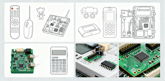
Single sided PCBs remain a popular choice for applications where simplicity, low cost, and ease of mass production are top priorities. These boards are commonly found in basic electronic devices, toys, calculators, and household appliances, where the circuit design is straightforward and the component density is relatively low. Single sided PCBs are also widely used in LED lighting and simple sensors, offering a cost effective solution for products that do not require the complexity of double sided PCBs.
Because single sided PCBs use fewer materials and have a simpler manufacturing process compared to double sided PCBs, they are ideal for high-volume production runs and applications where minimizing costs is essential. Their straightforward design makes them well-suited for modern devices that prioritize reliability and affordability over advanced functionality. For projects where a simple circuit design and low component density are sufficient, single sided PCBs provide an efficient and economical option, helping manufacturers deliver quality electronic devices at a competitive price.
Future Development Trends
As electronic devices evolve toward miniaturization and high performance, double-side assembly technology is becoming increasingly common. Emerging technologies such as buried and blind via technology and rigid-flex board technology are further advancing the development of PCB assembly technology.
These technologies combine the advantages of single and double-side assembly to achieve higher circuit density and performance within limited space.
Conclusion
Choosing between single-side and double-side PCB assembly ultimately comes down to finding the right balance between cost, complexity, and performance. Single-side assembly is suitable for relatively simple circuits and cost-sensitive applications, while double-side assembly is appropriate for high-density circuits, space-constrained designs, and electronic products with high-performance requirements.
Regardless of which approach you choose, good design practices and close communication with manufacturers are key to ensuring the quality of the final product. By deeply understanding the characteristics, advantages, and limitations of single-side and double-side assembly, you can make more informed decisions in your product designs and create more competitive electronic products.
Do you have experience with PCB assembly design? Welcome to share your insights and questions in the comments section!
Author: Jack Wang

