


Chip-Package-PCB Co-Design for High-Performance Electronics
In modern electronics, the boundary between chip, package, and PCB is no longer a clean handoff—it’s a tightly connected ecosystem where every layer influences the next. As devices push for higher speeds, greater power density, and smaller form factors, even minor mismatches in electrical behavior, thermal flow, or mechanical stress can ripple across the entire system. Achieving reliable, high-performance products now depends on understanding how these three domains interact, and designing them as a unified whole. Chip–package–PCB co-design has emerged as the approach that turns this complexity into predictable, optimized performance, enabling engineers to reach system-level goals with fewer iterations and more confidence.
Why Chip–Package–PCB Co-Design Matters
Limitations of the Traditional, Segmented Design Approach
Traditional electronics design often treats the chip, the package, and the PCB as separate stages. Each team works independently, passing requirements downstream only after finishing its own portion. This segmented workflow creates several inherent problems.
First, it leads to multiple design iterations and a high rework rate. When electrical, thermal, or mechanical issues appear at the board level, engineers often discover that the root cause lies in chip I/O placement or package routing—elements that are expensive to revise once the upstream design is finalized. A single late-stage issue can force the entire design chain to cycle back to the beginning.
Second, signal integrity, power integrity, and thermal issues are difficult to identify early. Because the chip, package, and PCB are modeled separately, parasitics and interactions between layers remain hidden until system-level testing. For high-speed interfaces like PCIe or DDR, or for high-power devices such as AI accelerators, this delay can cause unexpected eye-diagram collapse, PDN noise, or localized overheating.
Third, system-level performance becomes harder to optimize. Even if each domain meets its own specifications, the combined system may fail to achieve the required bandwidth, jitter margin, power stability, or junction temperature. Without unified analysis, engineers can only fix issues reactively instead of designing proactively.
What Co-Design Solves
Chip–package–PCB co-design addresses these challenges by evaluating all three domains as a single system rather than isolated elements.
It enables system-level optimization of electrical performance, thermal performance, and mechanical reliability. By examining the complete signal path—from the chip buffer, through the package substrate, down to PCB routing—engineers can accurately predict losses, return paths, impedance changes, and hotspot locations. This approach improves the final design margin and reduces risk.
Co-design also shortens the design cycle and lowers overall cost. Early modeling of parasitics, heat transfer, and mechanical stress prevents cascading errors that lead to repeated redesigns. Teams can make informed decisions on I/O assignment, package structure, and PCB stack-up before committing to fabrication.
Finally, this methodology supports the needs of modern high-density, high-speed, and high-thermal-load products, including AI processors, 5G communication modules, automotive electronics, and multi-chip SiP or chiplet-based systems. These applications demand tight coordination across electrical, thermal, and mechanical domains—something only a co-design strategy can provide.
Through unified modeling and early collaboration, chip–package–PCB co-design transforms complexity into predictable performance and enables next-generation electronic systems to meet their aggressive technical targets.
Chip–Package–PCB Co-Design Overall Process
Information Input and Requirements Analysis
The foundation of an effective co-design starts with comprehensive requirements gathering. Engineers must analyze the product function, intended operating environment, and technical specifications to ensure the system meets its performance goals.
Next, the chip-level constraints are defined, including I/O configuration, target data rates, and power consumption. This helps determine how signals will travel through the package and PCB, as well as the thermal load the system must handle.
At the PCB level, technical capabilities such as layer count, dielectric material, via structure, and impedance control are assessed. Understanding these parameters early prevents downstream incompatibilities and enables better alignment between chip, package, and board design.
By capturing all these inputs, the team establishes a shared design baseline for electrical, thermal, and mechanical performance expectations, ensuring that subsequent modeling and simulation are meaningful and predictive.
System-Level Modeling and Simulation Chain Setup
Once requirements are defined, engineers construct accurate models for each domain:
Chip models: SPICE or IBIS models capture transistor-level behavior and I/O buffer characteristics.
Package models: RLCG and S-parameter representations describe parasitic resistance, inductance, capacitance, and signal loss within the package.
PCB models: RLGC and S-parameter models define trace impedance, crosstalk, and power delivery characteristics.
These models are then combined to form a complete system-level simulation chain, including signal paths and power delivery networks. This allows engineers to evaluate how a signal travels from the chip transmitter (TX), through the package substrate, across the PCB, to the chip receiver (RX). For example, a PCIe 5.0 channel can be modeled from the TX buffer on the chip, through BGA package traces, via the PCB route, to the RX, revealing losses, reflections, and timing margins.
By integrating these models, potential issues such as signal degradation, voltage drop, or hotspot formation can be identified early—long before physical prototypes exist.
Results-Driven Iterative Optimization
Simulation results form the basis for iterative design adjustments. Engineers can fine-tune:
Chip I/O assignment to optimize trace lengths and minimize crosstalk
Package layout and bump/pad configuration to reduce parasitics
PCB topology, including layer stacking, via placement, and trace routing
Electrical, thermal, and mechanical pathways are optimized simultaneously to ensure system-level performance targets are met.
The final outcome is a set of verified design parameters and manufacturing-ready files, covering chip pinout, package layout, PCB stack-up, and routing instructions. This approach minimizes redesign risk, accelerates time-to-market, and ensures that the chip–package–PCB ecosystem functions as a cohesive system.
1. Electrical Co-Design (Signal + Power Integrity)
1. Chip-Level Design Requirements
The first step in electrical co-design begins at the chip level, where I/O configuration and interconnect strategy significantly influence overall system performance.
I/O Arrangement Optimization: Proper assignment of chip I/Os reduces trace length imbalance, minimizes crosstalk, and improves signal timing. For example, DDR5 memory chips benefit from grouping data and strobe signals to maintain matched lengths and reduce reflections.
Interconnect Choice: Selection between wire bonding and flip-chip impacts parasitic inductance and capacitance. Flip-chip reduces bond wire parasitics and enables shorter signal paths, improving high-speed performance.
Reducing Packaging Complexity: Minimizing the number of high-speed nets crossing the package or optimizing bump/pad placement can lower parasitic effects. This approach reduces insertion loss and preserves signal integrity.
By addressing these factors at the chip stage, designers create a foundation for more predictable package and PCB performance.
2. Package Electrical Design Strategy
The package acts as the bridge between chip and PCB, and its design is critical for maintaining signal and power quality.
Package Type Selection: Options include BGA, LGA, QFN, and SiP. Choice depends on signal density, thermal performance, and mechanical constraints.
RLC Parasitic Optimization: Designers model resistance, inductance, and capacitance within the package to minimize signal degradation and cross-talk.
Power/Ground Network (PDN) Design: Effective distribution of power planes, decoupling capacitors, and localized power islands ensures a low-impedance power network, reducing voltage fluctuations and noise.
Signal Return Path Management: Package layout must maintain proper return paths for high-speed signals, avoiding loops that could cause EMI or signal distortion.
Optimized package design directly affects board-level routing, signal quality, and system reliability.
3. PCB Electrical Design Key Points
PCB design completes the signal and power integrity chain. Critical considerations include:
High-Speed Routing Rules: Maintain length matching, impedance control, and optimized via placement. For differential pairs, ensure proper spacing to preserve characteristic impedance.
Reference Plane Integrity: Continuous ground and power planes minimize loop inductance and reduce EMI. Broken planes can lead to signal reflections and crosstalk.
Board-Level PDN and Noise Management: Implement low-impedance power networks, carefully place decoupling capacitors, and use targeted filtering to reduce simultaneous switching noise (SSO).
A well-designed PCB ensures that signals arrive with minimal distortion and power delivery remains stable under dynamic load conditions.
4. Collaborative Simulation Methods
Electrical co-design relies on system-level simulation to capture interactions across chip, package, and PCB.
SI/PI Tools: Software such as Sigrity or Ansys SIwave enables signal integrity (SI) and power integrity (PI) analysis at the system level.
Multi-Domain Modeling: Combine SPICE models (chip), S-parameters (package), and geometric PCB models for realistic simulations.
Coupling Path Analysis: Evaluate crosstalk, return path discontinuities, and simultaneous switching output (SSO) noise, identifying potential issues before fabrication.
Step-by-step simulation allows designers to iteratively refine chip I/O, package layout, and PCB topology to meet system-level performance goals.
5. Measurable Metrics
To quantify electrical performance, several metrics are commonly used:
Eye Diagrams: Visualize signal integrity, revealing timing jitter and amplitude margin.
Return Loss and Insertion Loss: Measure signal attenuation and reflections across high-speed channels.
PDN Z-Profile: Assess impedance stability of the power delivery network over frequency.
Timing Margin: Calculate setup and hold time margins for critical interfaces.
Typical validation includes USB4, PCIe, and DDR5 channel verification, ensuring that the combined chip-package-PCB system meets high-speed compliance standards.
2. Thermal Co-Design
1. Chip Power and Thermal Density Analysis
Thermal co-design begins by understanding the power consumption and heat density of the chip or multi-chip system.
Single-Chip vs. Multi-Chip Power Data: Engineers gather detailed specifications for each chip, including average and peak power, dynamic vs. static power contributions, and expected duty cycles. Multi-chip systems, such as AI accelerators or SiP modules, often present localized hotspots that require targeted cooling.
Heat Sources and Peak Temperature Distribution: Identify which areas of the chip generate the most heat—typically high-frequency logic blocks, memory arrays, or power management circuits. Mapping peak junction temperatures (Tj) helps guide package and board thermal strategies.
Example: An AI accelerator may have high thermal density in a small area compared to an edge computing chip, which spreads power across a larger die. This comparison informs whether localized heat sinks or system-level cooling is required.
2. Package-Level Thermal Optimization
The package plays a crucial role in transporting heat from the chip to the PCB or external heatsink.
Internal Heat Slug: Many packages, including FCBGA and SiP, use a metal heat slug directly above the die to efficiently conduct heat away from the chip.
Copper Pillars, Thermal Vias, and Mold Materials: Optimizing these elements reduces thermal resistance from die to PCB. Copper pillars and thermal vias provide low-resistance paths for vertical heat flow, while mold compounds with high thermal conductivity improve lateral spreading.
Thermal Interface Materials (TIM): Selecting the right TIM between chip, heat slug, and package lid improves thermal contact. Engineers compare thermal conductivity, thickness, and reliability to choose optimal materials.
Typical Path Example: In an FCBGA or SiP package, heat flows from the die to the heat slug, through thermal vias in the substrate, and into the PCB or external heatsink.
3. PCB-Level Thermal Design Methods
The PCB can further enhance system cooling when designed with thermal considerations in mind.
Metal Core and Thick Copper Layers: Metal-core PCBs or thick copper layers reduce thermal resistance, spreading heat more evenly across the board.
High Thermal Conductivity Materials: Materials like ceramic-filled resins or thermally conductive laminates improve heat transfer from package to board.
Board-Level Spreading Strategy: Techniques such as copper spreading planes help dissipate heat laterally, preventing local hotspots.
Cooling Interfaces: PCBs are often coupled with fans, heat sinks, or liquid cooling modules. Designing the interface early ensures efficient heat removal without interfering with signal integrity.
4. Thermal Simulation and Experimental Validation
Simulation and measurement confirm that thermal strategies meet system requirements.
Junction Temperature Prediction (Tj): Thermal models estimate Tj under expected operating conditions.
Thermal Resistance Network Models (Rjc, Rjb, Rja): These metrics quantify resistance from junction-to-case, junction-to-board, and junction-to-ambient, providing a clear picture of thermal pathways.
Multi-Chip Package Temperature Distribution: Simulation visualizes hotspots across die and package, guiding adjustments to heat sinks, vias, or copper spreading.
Experimental Verification: Real-world testing with infrared thermography or thermocouples validates simulation accuracy and identifies any discrepancies, ensuring reliable thermal performance.
3. Thermo-Mechanical Reliability Co-Design
1. Sources of Stress and Failure Models
Thermo-mechanical reliability focuses on how mechanical stress induced by temperature changes affects chips, packages, and PCBs. Key stress sources include:
CTE Mismatch and Thermal Cycling Fatigue: Different coefficients of thermal expansion (CTE) between the die, package, and PCB can generate repeated stress during temperature cycles, leading to solder joint fatigue.
Package Warpage: Uneven thermal expansion can cause warpage, which strains solder joints and reduces mechanical reliability.
Common Failures: Thermal stress can trigger solder ball fatigue, package cracking, or delamination between layers, compromising both electrical and structural integrity.
Understanding these failure mechanisms allows engineers to design proactively for system longevity.
2. Simulation and Analysis Methods
Predicting thermo-mechanical behavior relies on computational modeling and material characterization:
Node-Level Stress and Strain Analysis: Finite Element Analysis (FEA) simulates stress distribution across the chip, package, and PCB layers.
Material Property Parameters: Key inputs include Young’s modulus (E), CTE, and Poisson’s ratio, which define how each material responds to thermal and mechanical loads.
Layer-by-Layer Thermal Stress Simulation: Multi-layer modeling captures how heat-induced expansion in one layer affects others, critical for high-density or multi-chip packages.
Example: FEA can predict BGA solder ball fatigue life, allowing designers to modify layout or materials before fabrication.
3. Structural and Material Optimization Strategies
Reliability can be improved through material selection and structural design:
Thermal Expansion Matching: Use low-CTE materials or composite substrates to reduce stress between die, package, and PCB.
Package Support Enhancement: Techniques like underfill, corner bonding, or mechanical stiffeners strengthen solder joints and reduce warpage.
Warping Mitigation in Package/PCB Design: Design rules, such as symmetrical layer stacking or copper balancing, help control deformation.
Multi-Chip Systems (Chiplets): Distribute mechanical loads carefully in SiP or chiplet designs to prevent localized stress accumulation.
4. Reliability Testing and Validation
Simulations are validated through standardized tests to ensure real-world performance:
Temperature Cycling Test (TCT): Measures fatigue and solder joint life under repeated heating and cooling cycles.
Power Cycling Test (PCT): Evaluates degradation under fluctuating electrical loads that generate localized heating.
Board-Level Drop Test: Assesses mechanical shock resistance for portable or automotive applications.
Failure Analysis Tools: Techniques like X-ray imaging, C-SAM, or SEM identify solder cracks, delamination, or internal package defects.
By combining modeling with experimental validation, engineers ensure that chips, packages, and PCBs meet reliability standards across thermal and mechanical stress conditions.
4. Toolchain and Implementation Recommendations for Co-Design
1. EDA Toolchain
Effective chip–package–PCB co-design relies on a comprehensive set of EDA tools tailored for each domain and for system-level integration:
Chip-Level Tools: Cadence Virtuoso and Synopsys HSPICE provide circuit-level simulation, including transistor behavior, timing analysis, and power modeling. These tools allow engineers to optimize I/O placement, buffer characteristics, and on-chip power distribution before integrating with package or PCB.
Package Design Tools: Xpedition Substrate and Allegro Package Designer enable parasitic extraction, bump/pad layout optimization, and power/ground network design within BGA, LGA, or SiP packages.
PCB Tools: Allegro, Altium, and Zuken support routing, layer stack-up planning, impedance control, and PDN design. They also facilitate collaboration between signal, power, and thermal engineers.
System-Level Simulation Tools: Sigrity, Ansys, and Keysight ADS combine models from chip, package, and PCB domains to perform signal integrity, power integrity, and thermal-mechanical analysis at the system level, enabling early detection of cross-domain issues.
Using a coordinated toolchain ensures seamless data exchange and consistent modeling across all design stages.
2. Data Interfaces and Model Management
Smooth co-design requires structured model management and standardized data exchange:
Model File Types: SPICE and IBIS for chip electrical behavior, S-parameters for package and PCB signal paths, and 3D models for thermal and mechanical simulation.
Version Control and Collaboration: Maintain strict versioning and file tracking to prevent conflicts. Implement cross-team review checkpoints to ensure all stakeholders work from the latest validated models.
Example: A Chip-Package-Board co-design data flow begins with SPICE/IBIS extraction from the chip, passes through package parasitic modeling, and integrates into PCB layout simulation, maintaining traceability at each stage.
Proper model management enables accurate multi-domain simulations and reduces design errors caused by inconsistent or outdated files.
3. Design Team Collaboration Practices
Successful co-design is as much about process as it is about tools:
Synchronized Teams: Chip, package, and PCB engineers must work in parallel, sharing requirements, constraints, and simulation feedback in real time.
DFx Guidelines: Establish DFA (Design for Assembly), DFM (Design for Manufacturability), and DFT (Design for Test) principles to align teams on manufacturability, reliability, and testability objectives.
Cross-Team Review Checkpoints: Schedule regular design reviews at critical milestones—e.g., post-chip I/O optimization, post-package layout, pre-PCB fabrication—to validate alignment and resolve conflicts early.
Step-by-Step Example: During a DDR5 channel project, the chip team shares IBIS models with the package team. The package team optimizes bump placement and sends updated S-parameters to the PCB team, who then finalize routing and layer stack-up. A system-level simulation validates signal and power integrity before fabrication.
By combining a robust EDA toolchain, disciplined model management, and synchronized collaboration, teams can achieve efficient, reliable chip–package–PCB co-design, reducing iteration cycles and ensuring predictable system-level performance.
5. Typical Application Scenarios and Case Studies
1. High-Speed Interface Products
High-speed interfaces such as PCIe 5.0/6.0, USB4, and SerDes channels demand strict signal and power integrity.
Challenges Addressed: At these data rates, signal integrity degradation, channel loss, and improper return paths can severely limit performance. Without co-design, reflections, crosstalk, and eye diagram closure may occur, causing data errors or protocol failures.
Example: In a PCIe 5.0 link, co-design ensures that chip I/O placement, package parasitics, and PCB trace routing work together to maintain target insertion loss and minimize jitter. Using system-level simulations, engineers can optimize trace lengths, differential pair spacing, and return paths before fabrication.
By applying chip–package–PCB co-design, high-speed products achieve reliable eye openings and compliance with high-speed standards, reducing redesign risk.
2. High Power-Density Chips
Modern AI accelerators and power semiconductors generate significant heat in compact die areas, requiring innovative thermal solutions.
Challenges Addressed: High thermal density can lead to hotspots, junction overheating, and accelerated material degradation. Traditional design methods may fail to predict these effects.
Thermal Solutions: Co-design integrates package heat slugs, thermal vias, and PCB copper spreading with active cooling methods. Materials like high-conductivity mold compounds and advanced TIMs are selected to minimize thermal resistance.
Example: An AI accelerator with multiple high-frequency cores used vertical thermal vias combined with a heat slug in the SiP package, reducing peak junction temperature by 15°C compared to standard package designs.
Thermal co-design ensures that power-dense chips operate reliably under full load without compromising performance or lifespan.
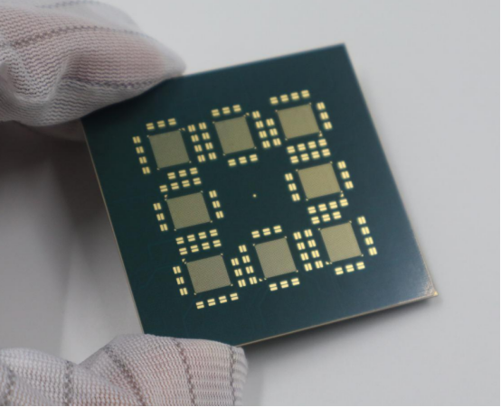
3. Multi-Chip Integrated Systems (SiP / Chiplet)
Multi-chip modules such as SiP or chiplet-based systems introduce additional complexity in electrical, thermal, and mechanical domains.
Challenges Addressed: High interconnect density, close chip spacing, and mismatched thermal expansion coefficients create signal routing bottlenecks, thermal hotspots, and mechanical stress.
Co-Design Solutions: System-level packaging is optimized alongside PCB design to align interconnect layers, balance thermal loads, and manage mechanical stress. Techniques include micro-bumps, embedded substrates, and staggered die placement to simplify routing and reduce stress concentrations.
Example: A multi-chip AI SiP combined advanced packaging with PCB copper spreading and thermal vias, achieving both signal integrity compliance and effective heat dissipation across multiple die in a compact form factor.
By addressing electrical, thermal, and mechanical interactions simultaneously, co-design enables high-performance, reliable multi-chip systems that would be difficult to achieve with isolated design approaches.
Conclusion
Co-design of chip, package, and PCB delivers measurable value across electrical, thermal, and thermo-mechanical dimensions. By optimizing signal integrity, power delivery, heat dissipation, and mechanical reliability simultaneously, engineers can achieve higher system performance while preventing issues that might arise from isolated design approaches. For example, aligning chip I/O placement with package parasitics and PCB routing can preserve high-speed channel performance, while integrated thermal strategies reduce hotspots in high-power devices like AI accelerators.
This collaborative methodology also reduces development risk and overall cost. Early simulation and iterative optimization minimize the need for multiple prototyping cycles, prevent late-stage design changes, and ensure predictable system behavior. Companies leveraging this approach, such as PCBMASTER, can provide clients with optimized, manufacturable designs that meet aggressive performance and reliability requirements.
Finally, chip–package–PCB co-design supports the evolution of high-performance electronics. As AI, 5G, automotive, and multi-chip systems demand higher speed, density, and power efficiency, a coordinated design strategy becomes essential. By embracing co-design principles, engineers are better equipped to deliver cutting-edge products that push the boundaries of technology while maintaining reliability and cost-effectiveness.
FAQs
What is Chip–Package–PCB Co-Design, and What Advantages Does It Have Over Traditional Design?
Chip–Package–PCB co-design is a holistic approach that treats the chip, its package, and the PCB as an interconnected system rather than isolated stages. Unlike traditional segmented design, where each domain is optimized independently, co-design ensures that electrical performance, thermal management, and mechanical reliability are considered simultaneously.
Advantages include:
Improved system-level performance: Signal integrity, power integrity, and thermal behavior are optimized across the entire signal path.
Reduced design iterations and costs: Early detection of cross-domain issues avoids expensive late-stage rework.
Support for high-density, high-speed, and high-power applications: Modern products such as AI accelerators, 5G modules, and automotive electronics benefit from coordinated design strategies.
Which Model Files Are Most Critical in Co-Simulation?
In chip–package–PCB co-simulation, accurate models are essential for predicting system behavior:
SPICE: Captures detailed transistor-level or circuit-level electrical behavior, used primarily for chip-level analysis.
IBIS: Models I/O buffer behavior for signal integrity simulation, bridging chip to package.
S-Parameters: Represent package and PCB frequency-dependent behavior, including insertion loss, return loss, and crosstalk.
3D Mechanical/Thermal Models: Optional but critical for thermal and thermo-mechanical co-simulation, capturing heat flow and stress distribution.
These files allow engineers to simulate electrical, thermal, and mechanical interactions across the entire system before fabrication.
How Do Package and PCB Thermal Designs Work Together to Reduce Junction Temperature?
Effective thermal co-design requires coordinated heat paths from the chip to the environment:
Package Level: Use heat slugs, thermal vias, and high-conductivity mold compounds to extract heat from the die efficiently.
PCB Level: Employ thick copper layers, metal-core boards, or high-conductivity laminates to spread heat, combined with strategically placed thermal vias.
Integrated Strategy: The package’s thermal vias should align with PCB copper planes and external heatsinks, enabling direct heat transfer and lowering peak junction temperature (Tj).
How Can We Determine If Package and PCB Structures Will Cause Solder Joint Fatigue?
Thermo-mechanical reliability is assessed using a combination of simulation and testing:
FEA (Finite Element Analysis) models stress and strain across solder balls, package, and PCB layers under thermal cycles.
Material Properties: Young’s modulus, CTE, and Poisson’s ratio help predict deformation and stress.
Experimental Validation: Temperature cycling tests (TCT), power cycling tests (PCT), and X-ray or C-SAM inspection detect solder cracks or delamination.
By comparing predicted stress levels to allowable solder fatigue limits, engineers can identify designs at risk of failure.
How Are Multi-Chip Systems (SiP/Chiplet) Effectively Co-Designed for Electrical and Thermal Performance?
Multi-chip modules introduce higher interconnect density and thermal complexity. Effective co-design strategies include:
Electrical: Optimize chip placement, bump/pad layout, and PCB routing to minimize signal loss, crosstalk, and mismatched return paths. System-level simulations integrate SPICE, IBIS, and S-parameter models for each chip.
Thermal: Use staggered die placement, aligned thermal vias, heat slugs, and copper spreading to balance power density and prevent hotspots. TIM selection and package-to-board thermal alignment are critical.
Mechanical: Underfill, corner bonding, and careful substrate selection reduce warpage and solder fatigue in high-density assemblies.
Through coordinated electrical, thermal, and mechanical modeling, multi-chip systems achieve reliable performance even in compact, high-speed packages.

