


What Is PCBA and Its Components? A Complete Guide for Beginners
From smartphones that fit in your palm to satellites orbiting Earth, every piece of modern technology relies on one silent powerhouse — the PCBA. It’s the hidden heart of electronic devices, turning static circuit boards into intelligent, functioning systems. Though it often goes unnoticed, understanding what a PCBA is and how its tiny components work together opens a fascinating window into how today’s electronics come to life.
Introduction to PCBA
What Does PCBA Stand For?
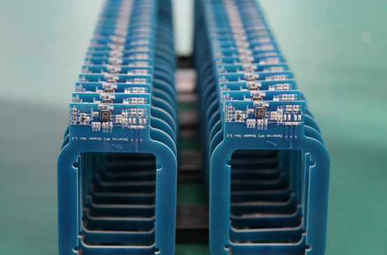
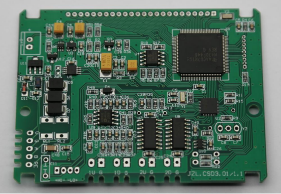
PCBA stands for Printed Circuit Board Assembly, which refers to a complete electronic board after all components are mounted on a bare PCB. The base PCB only provides the structure and copper pathways that connect different points. Once resistors, capacitors, ICs, and connectors are soldered onto it, it becomes a fully functional PCBA capable of powering electronic systems.
The difference between a PCB and a PCBA is straightforward but crucial. A PCB (Printed Circuit Board) is the empty board made of layers of fiberglass, copper, and solder mask — it cannot perform any electronic function on its own. A PCBA, on the other hand, is the assembled version, ready to operate once it’s connected to power or integrated into a device.
Within the electronics manufacturing process, PCBA sits at the assembly and testing stage. After a PCB is fabricated, manufacturers use Surface Mount Technology (SMT) or Through-Hole Technology (THT) to mount components, followed by soldering and inspection. This transformation from a blank board to a working circuit makes PCBA the bridge between electronic design and functional hardware.
Why PCBA Is Important in Modern Electronics
Every modern electronic device — from a smartphone to an electric vehicle control module — depends on a PCBA to connect, support, and coordinate electronic components. The PCBA acts as the central nervous system of any electronic product, ensuring that electrical signals flow accurately between chips, sensors, and power circuits.
In practical terms, PCBAs make it possible for:
Smartphones to process data, manage power, and connect wirelessly.
Automotive systems to control safety features like ABS or engine management.
Medical devices such as ECG monitors or imaging equipment to deliver precise and reliable readings.
Beyond connectivity, PCBAs directly influence a product’s performance, reliability, and size. High-density designs and multi-layer assemblies enable miniaturization without compromising signal integrity. Meanwhile, precision soldering and automated inspection processes ensure long-term durability, even in harsh environments.
In essence, PCBA is the foundation of functional electronics, transforming conceptual designs into intelligent, high-performance devices that power everyday life.
Understanding the Difference Between PCB and PCBA
What Is a PCB (Printed Circuit Board)?
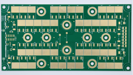
A PCB, or Printed Circuit Board, is the foundation of any electronic device, serving as the physical platform that connects and supports electronic components. It is made up of several layers, including a substrate (base material), copper traces, and a solder mask that protects the conductive pathways.
The substrate material gives the PCB its rigidity and thermal stability. The most common material is FR-4, a glass-reinforced epoxy laminate known for its strength and insulation properties. For high-frequency or high-speed applications, advanced materials like Rogers or polyimide are used because they offer better signal performance and heat resistance.
Each layer of copper on the PCB forms electrical circuits or traces that connect various points, allowing current to flow between components once assembly begins. However, on its own, a PCB is non-functional — it only becomes operational after components are added during the assembly process.
What Is a PCBA (Printed Circuit Board Assembly)?
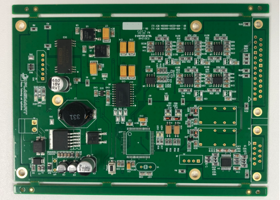
A PCBA (Printed Circuit Board Assembly) is the next stage after PCB fabrication, where all electronic components are mounted and soldered onto the bare board. This process turns a static circuit board into a fully functional electronic module.
The assembly process involves two main technologies:
Surface Mount Technology (SMT) – Components are placed directly onto the surface of the PCB and soldered using reflow ovens. SMT is ideal for compact, high-density designs like smartphones and IoT devices.
Through-Hole Technology (THT) – Components with leads are inserted into drilled holes and soldered on the opposite side. THT offers strong mechanical bonds, making it suitable for high-power or industrial applications.
Once components are mounted, the PCBA undergoes inspection and functional testing to ensure performance and reliability. This step completes the transformation from a simple board into an intelligent, working electronic assembly.
Comparison Table: PCB vs. PCBA
Feature
PCB (Printed Circuit Board)
PCBA (Printed Circuit Board Assembly)
Definition
The bare circuit board made of substrate and copper layers.
The finished board with all components soldered and functional.
Manufacturing Stage
Early stage — board fabrication only. Later stage — component assembly and testing.
Key Materials
FR-4, Rogers, Polyimide, Copper Foil.
Same PCB materials + electronic components (ICs, resistors, connectors).
Complexity
Structurally simple; design-focused.
More complex due to assembly, soldering, and quality control steps.
Functionality
Non-functional without components.
Fully functional and ready for integration into devices.
Cost Range
Lower (depends on layers and materials).
Higher (includes assembly, testing, and components).
Applications
Used as a base in circuit design and prototyping.
Used in final electronic products like smartphones, medical devices, and automotive systems.
Feature
PCB (Printed Circuit Board)
PCBA (Printed Circuit Board Assembly)
Definition
The bare circuit board made of substrate and copper layers.
The finished board with all components soldered and functional.
Manufacturing Stage
Later stage — component assembly and testing.
Key Materials
FR-4, Rogers, Polyimide, Copper Foil.
Same PCB materials + electronic components (ICs, resistors, connectors).
Complexity
Structurally simple; design-focused.
More complex due to assembly, soldering, and quality control steps.
Functionality
Non-functional without components.
Fully functional and ready for integration into devices.
Cost Range
Lower (depends on layers and materials).
Higher (includes assembly, testing, and components).
Applications
Used as a base in circuit design and prototyping.
Used in final electronic products like smartphones, medical devices, and automotive systems.
In short, a PCB provides the structure, while a PCBA delivers the function. Understanding this distinction helps engineers and buyers communicate effectively during design, production, and sourcing — ensuring the final product meets both performance and manufacturing goals.
Key Components of PCBA
Passive Components
Passive components are the building blocks that control the flow of electrical signals without generating energy themselves. The three main types are resistors, capacitors, and inductors.
Resistors regulate current and voltage within a circuit by providing precise resistance. For example, they help prevent sensitive components like LEDs from burning out by limiting current flow.
Capacitors store and release electrical energy when needed. They stabilize voltage, filter noise, and smooth power delivery in devices like power supplies and audio circuits.
Inductors store energy in magnetic fields and are essential for managing signal filtering and energy transfer in power converters or radio frequency circuits.
Together, these passive parts form the foundation of circuit stability and signal integrity, ensuring smooth and predictable electrical behavior.
Active Components
Active components are electronic devices that control current flow and amplify signals using external power sources. The key active parts on a PCBA are integrated circuits (ICs), diodes, and transistors.
Integrated Circuits (ICs) are complex miniaturized circuits embedded in a single chip. They perform various functions such as data processing, signal amplification, and logic control — for example, the microprocessor in a smartphone or the control IC in a power supply.
Diodes allow current to flow in only one direction, protecting circuits from reverse voltage and enabling rectification in power converters.
Transistors act as switches or amplifiers. In modern PCBAs, they are crucial in regulating voltage, driving signals, and forming the core of digital logic systems.
Active components essentially give a PCBA its intelligence and control, transforming passive circuits into responsive, functional systems.
Connectors and Interfaces
Connectors and interfaces provide the physical and electrical pathways that link a PCBA to other components, boards, or external devices. They enable both communication and power transfer across systems.
Common connector types include:
USB (Universal Serial Bus) for data transfer and power delivery in consumer electronics.
HDMI (High-Definition Multimedia Interface) for transmitting high-resolution audio and video signals.
Board-to-board connectors for linking multiple PCBAs within a single product, such as in modular control systems or multi-layer assemblies.
Reliable connectors are critical for signal integrity and mechanical stability, especially in high-speed or vibration-prone environments. Poor connector design can lead to power loss, data errors, or premature wear, making this component group vital for long-term reliability.
Other Essential Elements
Beyond standard passive and active parts, several specialized components ensure the PCBA’s precision, stability, and performance.
Crystals and Oscillators generate accurate clock signals that synchronize digital systems like microcontrollers or communication modules.
Transformers adjust voltage levels and isolate circuits, improving safety and power efficiency in devices such as chargers or converters.
Sensors convert physical parameters (like temperature, pressure, or motion) into electrical signals for smart device feedback and automation.
Heat Sinks dissipate excess heat from power components and processors, maintaining stable operation and preventing damage.
Each of these elements contributes to the functionality, efficiency, and reliability of the final electronic product, turning a simple circuit into a precisely engineered system capable of meeting modern performance demands.
The PCBA Manufacturing Process (Step-by-Step)
The PCBA manufacturing process transforms a bare PCB into a fully functional electronic assembly. Each step — from solder paste printing to final coating — requires precision, automation, and strict quality control. Below is a detailed, step-by-step breakdown of how a PCBA is made.
Step 1 – Solder Paste Printing
The process begins with applying solder paste onto specific areas of the PCB where components will be mounted. This is done using a stainless-steel stencil that aligns perfectly with the pad layout of the board.
The solder paste, a mixture of tiny solder particles and flux, acts as both an adhesive and a conductive bridge during soldering.
Precision is critical in this stage — even minor misalignment or uneven thickness can lead to solder bridging or weak connections later. High-end printers use automated vision alignment systems to ensure uniform coverage and consistent paste volume on every pad.
Step 2 – Component Placement
Once solder paste is applied, Surface Mount Technology (SMT) placement begins. This step uses automated pick-and-place machines to position tiny electronic components — resistors, capacitors, ICs, and more — onto their designated solder pads.
Modern SMT machines can place over 100,000 components per hour with incredible precision, often within ±0.05 mm. High-speed cameras verify each component’s orientation and value before placement, ensuring accuracy across mass production.
For boards with both SMT and Through-Hole components, hybrid assembly lines integrate robotic arms or manual operators for complex or large components not suited for automated placement.
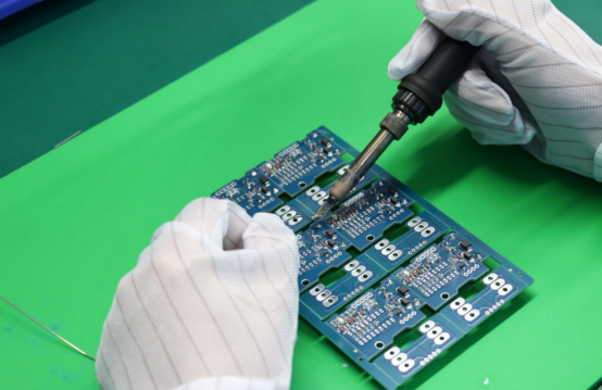
Step 3 – Soldering Process
After placement, the next stage is soldering, where components are permanently bonded to the board. The method depends on the component type:
Reflow Soldering (for SMT): The board passes through a reflow oven with precisely controlled temperature zones. The solder paste melts, forms joints, and then cools to create strong electrical and mechanical connections.
Wave Soldering (for THT): The board is passed over a “wave” of molten solder that coats and bonds the component leads inserted into drilled holes.
Common soldering defects include:
Solder bridges (unwanted connections between pads)
Tombstoning (small parts lifting on one end due to uneven heating)
Cold joints (insufficient heat or poor wetting)
Careful temperature profiling and process monitoring prevent these issues, ensuring reliable connections and long-term performance.
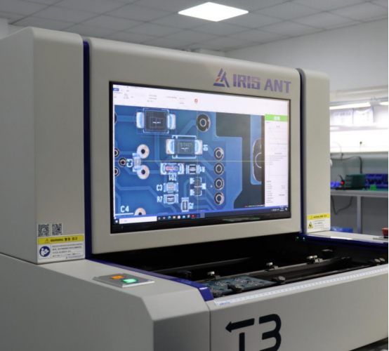
Step 4 – Inspection and Testing
After soldering, every board undergoes rigorous inspection and testing to ensure functionality and reliability.
Visual Inspection is used for simple boards or early prototypes.
AOI (Automated Optical Inspection) scans each board for missing components, solder defects, or polarity errors using high-resolution cameras.
X-ray Inspection is employed for complex assemblies with hidden joints, such as BGAs (Ball Grid Arrays).
For electrical validation, two main methods are used:
In-Circuit Testing (ICT): Checks individual component connections and circuit continuity.
Functional Circuit Testing (FCT): Verifies the overall performance of the assembled board under simulated operating conditions.
This multi-level testing ensures that only fully functional and defect-free assemblies move forward in production.
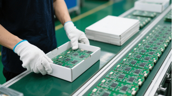
Step 5 – Cleaning and Final Assembly
After successful testing, PCBAs go through cleaning and finishing to prepare them for end-use.
During soldering, flux residues can remain on the board surface, potentially causing corrosion or short circuits. These are removed using aqueous, semi-aqueous, or vapor cleaning systems, depending on the board type and component sensitivity.
Next, for products exposed to harsh environments, the board may receive encapsulation or a conformal coating — a thin protective layer that shields against moisture, dust, and chemical exposure.
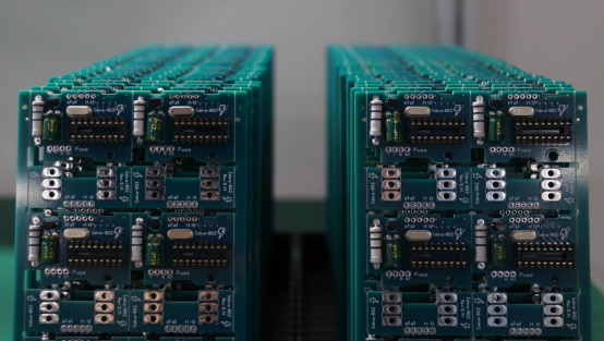
Finally, boards are assembled into their housings or enclosures, completing the PCBA manufacturing cycle — ready for integration into electronics ranging from smartphones and routers to industrial controllers and medical devices.
Each of these steps plays a vital role in determining the quality, reliability, and performance of the finished product. A well-controlled PCBA process not only improves yield and consistency but also extends the lifespan of the final electronic device.
Materials and Surface Finishes Used in PCBA
Common PCB Materials
The base material of a printed circuit board (PCB) determines its electrical performance, heat resistance, and durability. In PCBA manufacturing, several materials are used depending on the device’s design, cost, and operating environment.
FR-4 (Flame Retardant 4)
FR-4 is the most widely used PCB material, made from woven fiberglass and epoxy resin. It offers excellent mechanical strength, moisture resistance, and electrical insulation. FR-4 is ideal for general-purpose electronics such as computers, communication devices, and consumer gadgets.
Pros: Affordable, stable, and easy to process.
Cons: Limited for high-frequency or high-heat applications.
CEM-1 (Composite Epoxy Material 1)
CEM-1 combines paper core and epoxy resin to create a low-cost, single-layer board material. It’s commonly used in low-power devices and household appliances.
Pros: Economical and simple to fabricate.
Cons: Lower mechanical strength and poor heat resistance compared to FR-4.
Rogers Material
Rogers laminates are high-frequency PCB materials used in RF (radio frequency) and microwave applications. They have superior dielectric stability and low signal loss, making them ideal for 5G systems, radar, and aerospace electronics.
Pros: Excellent signal integrity and thermal management.
Cons: Higher material cost and more complex processing.
Polyimide
Polyimide is a flexible and heat-resistant material used in flexible and rigid-flex PCBs. It performs well in extreme temperatures and is often chosen for automotive, and aerospace applications.
Pros: High flexibility, thermal stability, and chemical resistance.
Cons: Expensive and slightly harder to manufacture than FR-4.
Each material type influences signal quality, thermal performance, and cost, so the selection must match the end product’s performance requirements and environmental conditions.
Popular Surface Finishes
A surface finish is the protective coating applied to the exposed copper pads on a PCB. It prevents oxidation, enhances solderability, and ensures reliable electrical connections during assembly. Choosing the right surface finish affects both cost and performance in PCBA production.
ENIG (Electroless Nickel Immersion Gold)
ENIG is a two-layer finish with a nickel barrier and a thin layer of gold on top. It provides a flat, durable, and oxidation-resistant surface, ideal for fine-pitch components and long shelf life.
Used in: High-reliability applications like aerospace, medical, and high-end consumer electronics.
Pros: Excellent solderability and corrosion resistance.
Cons: Higher cost compared to other finishes.
HASL (Hot Air Solder Leveling)
In HASL, the PCB is dipped into molten solder, then leveled with hot air to form an even coating. It is one of the most economical finishes, suitable for through-hole and general-purpose boards.
Used in: Consumer electronics and industrial control systems.
Pros: Low cost, good solder joint strength.
Cons: Uneven surface and limited compatibility with fine-pitch SMT components.
OSP (Organic Solderability Preservative)
OSP applies an organic layer that temporarily protects the copper surface from oxidation. It’s a lead-free, environmentally friendly option widely used in modern electronics.
Used in: Consumer devices and high-volume manufacturing.
Pros: Flat surface, low cost, RoHS-compliant.
Cons: Short shelf life and limited durability during multiple reflow cycles.
Immersion Silver
This finish uses a thin silver layer over copper to offer excellent electrical conductivity and smooth solderability. It’s a good balance between cost and performance, especially for high-speed signal transmission.
Used in: High-frequency and high-speed digital circuits.
Pros: Flat surface, good for fine-pitch components, stable conductivity.
Cons: Susceptible to tarnish and handling damage.
Comparison Summary:
Cost: HASL and OSP are the most affordable; ENIG and Rogers-based builds are the most expensive.
Solderability: ENIG and Immersion Silver provide the smoothest, most reliable solder joints.
Oxidation Resistance: ENIG offers the highest protection, while OSP requires careful handling.
In short, the combination of PCB base material and surface finish determines a board’s performance, longevity, and manufacturing efficiency — making material selection a critical step in achieving a reliable PCBA.
Quality Control and Testing in PCBA
Why Quality Control Matters
Quality control (QC) in PCBA is essential to ensure long-term reliability, reduce field failures, and comply with industry standards. A poorly inspected PCBA can lead to device malfunctions, costly recalls, or safety hazards. By implementing rigorous QC, manufacturers can identify defects early, maintain consistent product performance, and meet certifications such as IPC-A-610 for electronic assemblies or ISO 9001 for quality management.
For example, a smartphone with defective solder joints might fail after a few weeks, while a properly tested PCBA will function reliably for years. QC ensures that devices—from automotive control modules to medical monitoring equipment—perform safely and efficiently under real-world conditions.
Common Inspection Techniques
Several inspection methods are standard in PCBA manufacturing, each targeting different types of defects:
AOI (Automated Optical Inspection)
Uses high-resolution cameras and software algorithms to detect visible defects like missing components, misaligned parts, solder bridges, or insufficient solder. AOI is fast and ideal for high-volume SMT lines.
X-ray Inspection
Penetrates the PCB to identify hidden defects in BGA (Ball Grid Array) packages, internal vias, or solder joints that cannot be seen visually. X-ray is critical for multilayer and high-density boards where hidden faults can compromise performance.
ICT (In-Circuit Testing)
Applies electrical probes to measure component functionality, continuity, and signal integrity. ICT can detect open circuits, short circuits, and faulty components before the PCBA leaves the production line.
Using these methods together ensures that both visible and hidden issues are addressed, greatly reducing the risk of field failures.
Environmental and Reliability Testing
Beyond initial inspection, PCBA reliability must be validated under real-world environmental conditions. Common tests include:
Thermal Cycling
Alternates between high and low temperatures to simulate device operation in extreme climates. This helps detect thermal expansion or solder joint fatigue.
Vibration Testing
Subjects PCBAs to mechanical vibration to ensure components and solder joints can withstand shocks and movements, as seen in automotive or aerospace applications.
Humidity Testing
Exposes boards to high moisture levels to identify potential corrosion or delamination in components and substrates.
By performing these tests, manufacturers can guarantee that PCBAs remain functional and reliable even under harsh or fluctuating conditions, providing confidence to both engineers and end-users.
Quality control and rigorous testing are critical pillars of PCBA manufacturing, ensuring that electronic devices operate reliably, safely, and consistently over their lifespan.
Common Challenges and Best Practices in PCBA
Design for Manufacturability (DFM)
Design for Manufacturability (DFM) is the practice of designing a PCB with assembly and production in mind. A well-executed DFM ensures that a board can be assembled efficiently, reliably, and at lower cost. Poorly designed layouts can lead to soldering defects, component misalignment, and higher failure rates.
Examples of layout issues that often cause problems include:
Tightly spaced pads that increase the risk of solder bridges.
Long trace lengths for sensitive signals, which can introduce noise or delay.
Inconsistent pad sizes or via placements, making automated pick-and-place machines misalign components.
By applying DFM principles—such as proper pad sizing, adequate spacing, and standard component footprints—designers can minimize errors during assembly and improve overall yield.
Component Sourcing and Supply Chain Issues
Reliable component sourcing is critical for consistent PCBA production. Challenges include:
Shortages of high-demand or specialized components, which can delay production schedules.
Counterfeit or substandard parts, which risk device reliability and safety.
Lead time management, ensuring that components arrive in time to meet manufacturing deadlines without excessive inventory costs.
Best practices include establishing multiple suppliers, verifying component authenticity, and planning procurement based on demand forecasts. Proactive supply chain management helps maintain production continuity and prevents costly delays.
Minimizing Defects
Even with good design and sourcing, defects can occur during assembly. Effective strategies to minimize defects include:
Process Monitoring: Continuous inspection and testing during assembly catch defects early. AOI, ICT, and in-line monitoring help identify issues like poor solder joints or missing components.
Skilled Technicians: Experienced operators ensure precise component placement, handle rework correctly, and respond to unexpected issues efficiently.
Automation: Automated pick-and-place machines, reflow ovens, and soldering systems improve consistency, speed, and accuracy, reducing human error.
Combining these approaches ensures higher yields, improved reliability, and lower rework costs, resulting in PCBAs that meet performance and quality expectations consistently.
Overcoming challenges in PCBA manufacturing requires thoughtful design, careful sourcing, and rigorous process control. Following best practices helps manufacturers deliver reliable, high-quality PCBAs that perform well in demanding applications.
Future Trends in PCBA Technology
Miniaturization and High-Density Interconnects (HDI)
One of the most significant trends in PCBA technology is miniaturization, driven by consumer demand for smaller, lighter, and more powerful devices. High-Density Interconnect (HDI) PCBs enable this by using microvias, finer traces, and multiple layers to fit more components into a smaller footprint.
Technologies such as 5G smartphones, wearable devices, and IoT sensors rely heavily on HDI boards. For instance, a modern smartwatch requires a compact PCBA that integrates wireless communication, sensors, and processing power in a space smaller than a coin. Miniaturization not only reduces device size but also improves signal integrity and enables faster data transmission in high-speed applications.
Smart Manufacturing and Automation
The PCBA industry is increasingly embracing smart manufacturing, leveraging AI, robotics, and data analytics to improve production efficiency and product quality.
AI-powered inspection identifies defects in real-time, allowing faster corrections and reducing waste.
Robotic assembly lines enhance precision for high-density and complex boards, minimizing human error.
Data analytics enables predictive maintenance, process optimization, and yield improvement by analyzing trends from production metrics.
This automation ensures that manufacturers can produce high-quality PCBAs at scale, respond quickly to design changes, and maintain consistent reliability across batches.
Sustainable and Lead-Free PCBAs
Environmental considerations are reshaping PCBA manufacturing. Sustainable practices and lead-free soldering are becoming standard due to regulations such as RoHS (Restriction of Hazardous Substances).
Green initiatives include:
Using lead-free solders that meet RoHS compliance.
Reducing energy consumption during assembly with efficient reflow ovens and automated processes.
Recycling scrap materials and minimizing chemical waste in cleaning and coating steps.
Sustainable PCBAs not only protect the environment but also align with industry and consumer demand for eco-friendly electronics, making it a critical focus for manufacturers moving forward.
The future of PCBA technology is shaped by smaller, smarter, and greener designs. Miniaturization, automation, and sustainable practices together drive innovation, efficiency, and reliability, meeting the needs of next-generation electronics.
Conclusion
A Printed Circuit Board Assembly (PCBA) is more than just a circuit board—it is the heart of modern electronic devices, combining passive and active components, connectors, and specialized elements to create fully functional systems. Understanding each component and its role helps engineers, designers, and manufacturers ensure performance, reliability, and efficiency in electronics ranging from smartphones to medical devices.
Choosing a reliable PCBA manufacturer, such as PCBMASTER, is essential for achieving high-quality, high-performance assemblies. With expertise in advanced materials, precise assembly, and rigorous quality control, a trusted manufacturer ensures your electronic products meet both technical requirements and market expectations.
In short, knowledge of PCBA and careful selection of manufacturing partners are key steps toward building durable, efficient, and innovative electronics that stand out in today’s competitive market.
FAQs
What is the main difference between PCB and PCBA?
A PCB (Printed Circuit Board) is the bare board that provides the physical structure and copper traces for connecting electronic components. It cannot function on its own. A PCBA (Printed Circuit Board Assembly), on the other hand, is a PCB with all components—such as resistors, capacitors, ICs, and connectors—soldered onto it, making it a fully functional electronic module. In short, PCB is the foundation, while PCBA is the finished, working board.
What are the most common materials used in PCBA?
Common PCB materials include:
FR-4: Affordable and strong, suitable for general-purpose electronics.
CEM-1: Low-cost option for single-layer boards, often used in household devices.
Rogers: High-frequency material for RF and microwave applications, such as 5G devices.
Polyimide: Flexible and heat-resistant, used in flexible or high-temperature applications.
The choice of material affects signal quality, thermal performance, and durability of the PCBA.
How do you test the quality of a PCBA?
Quality testing in PCBA includes:
AOI (Automated Optical Inspection): Detects visual defects like missing components, misalignment, or solder bridges.
X-ray Inspection: Checks hidden solder joints and internal structures in multilayer or BGA boards.
ICT (In-Circuit Testing): Measures component functionality, continuity, and signal integrity.
Environmental and reliability tests: Thermal cycling, vibration, and humidity tests ensure the board can withstand real-world conditions.
These methods ensure reliable, defect-free PCBA performance.
What industries use PCBA the most?
PCBA is widely used across industries, including:
Consumer electronics: Smartphones, laptops, tablets, wearables.
Automotive: Engine control units, safety systems, infotainment.
Medical devices: Monitors, imaging equipment, diagnostic tools.
Industrial and aerospace electronics: Automation controllers, avionics, communication systems.
Essentially, any industry that relies on electronic devices or systems requires PCBA.
What trends will shape the future of PCB assembly?
Key trends in PCBA include:
Miniaturization and High-Density Interconnects (HDI): Smaller, more powerful boards for 5G, IoT, and wearable devices.
Smart manufacturing and automation: AI, robotics, and data analytics improving assembly precision and yield.
Sustainable and lead-free PCBA: Green manufacturing practices, RoHS compliance, and eco-friendly materials.
These trends drive smaller, smarter, and more reliable electronics for the next generation of technology.

