


Printed Circuit Board Assembly Process: A Step-by-Step Guide for Beginners
In the world of electronics, even the most innovative ideas rely on one hidden hero: the printed circuit board. These intricate boards serve as the backbone of every device, quietly connecting components and making complex systems work seamlessly. For beginners, stepping into the PCB assembly process can feel like entering a maze of tiny parts, precise machines, and meticulous techniques—but understanding it unlocks the power to bring electronic designs to life. From everyday gadgets to high-tech industrial equipment, mastering this process transforms concepts into functioning reality, revealing the fascinating craftsmanship behind every circuit.
Introduction to Printed Circuit Board (PCB) Assembly
What is PCB Assembly?
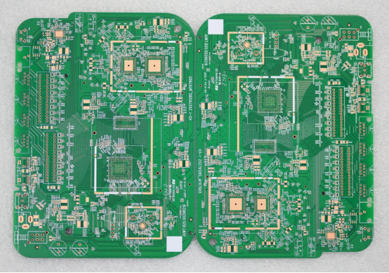
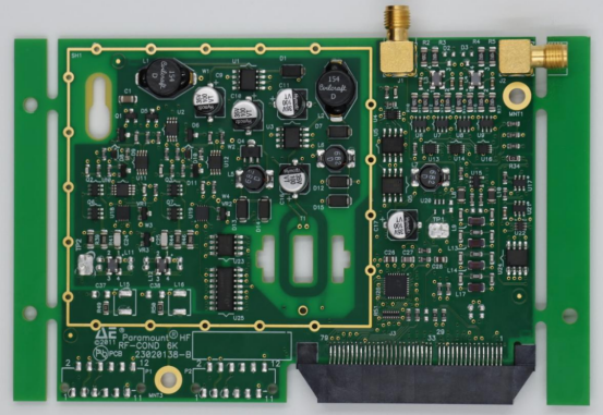
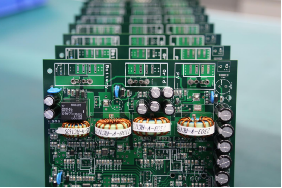
Printed Circuit Board (PCB) assembly is the process of attaching electronic components to a bare PCB to create a functional electronic circuit. While PCB fabrication produces the physical board with copper traces, holes, and layers, PCB assembly brings the board to life by mounting components such as resistors, capacitors, integrated circuits, and connectors.
In simple terms, fabrication is like building a blank canvas, and assembly is like painting a detailed picture on it. Without assembly, the PCB cannot perform any electronic functions. For example, a smartphone motherboard may have hundreds of tiny components soldered onto a fabricated PCB to enable functions like processing, communication, and power management.
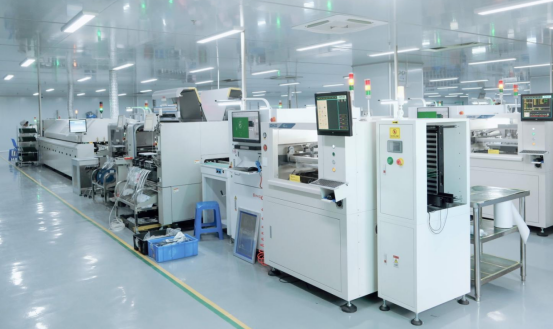
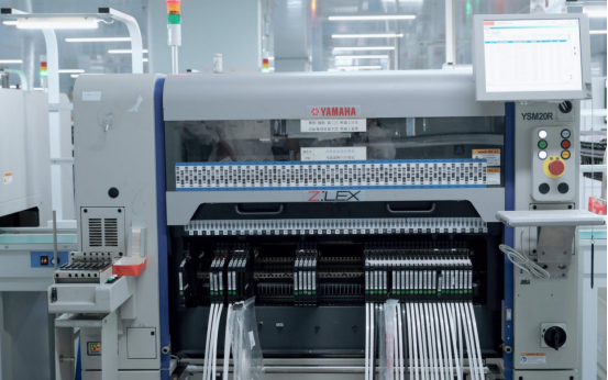
The assembly process can be automated using Surface Mount Technology (SMT) machines or done manually for specialized components, depending on the complexity of the circuit and production volume.
Importance of Understanding the PCB Assembly Process
Understanding PCB assembly is crucial for producing reliable, high-quality electronic devices. Poor assembly can lead to defects such as solder bridges, open circuits, or misaligned components, which can compromise product performance or cause complete device failure.
Different industries rely on PCB assembly in unique ways. In consumer electronics, precise assembly ensures gadgets like laptops, smartphones, and wearables work consistently. In the automotive sector, assembly quality affects critical systems such as engine control units and safety sensors. Industrial applications, like robotics or automation equipment, require assembly that can withstand harsh environments and long operational hours.
By understanding the assembly process, designers, engineers, and beginners can anticipate potential issues, optimize layouts, and choose appropriate assembly methods to ensure both functionality and durability.
Common Terminology in PCB Assembly
PCB assembly comes with specialized terms that are important to understand for beginners:
SMT (Surface Mount Technology): Components are mounted directly onto the surface of the PCB. Most modern electronics use SMT for its speed and compact design.
THT (Through-Hole Technology): Components have leads that go through holes in the PCB and are soldered on the opposite side. This method is often used for large or mechanical components.
Solder Mask: A protective layer applied to the PCB to prevent solder from bridging between conductive traces.
Stencil: A template used to apply solder paste accurately to specific areas of the PCB before placing SMT components.
Other common terms include BOM (Bill of Materials), reflow soldering, wave soldering, and pick-and-place machines. Knowing these terms helps beginners read assembly instructions, understand industry guides, and communicate effectively with manufacturers.
For example, a beginner might see a PCB labeled with “SMT resistors, THT capacitors, solder mask green, stencil pattern applied,” which describes exactly how the components are arranged and prepared for assembly.
Preparing for PCB Assembly
Reviewing PCB Design Files
Before starting assembly, it is essential to carefully review all PCB design files. Key files include Gerber files, which define the PCB’s copper layers, pads, and holes, and the Bill of Materials (BOM), which lists all components with specifications, quantities, and part numbers. Assembly drawings provide visual guidance on component placement and orientation.
During this review, identifying critical components—such as high-speed ICs, connectors, or polarized parts—is crucial. Special instructions, like specific soldering methods, thermal requirements, or testing notes, should be noted to prevent assembly errors. For example, an IC with fine-pitch leads may require careful SMT placement, while a large capacitor may need THT insertion.
Component Sourcing and Inspection
Sourcing high-quality components is a critical step in ensuring PCB reliability. Components should be purchased from verified suppliers with proper certifications to prevent counterfeit or low-quality parts. Checking component quality includes verifying part numbers, dimensions, polarity, and functionality.
Common components include integrated circuits (ICs), resistors, capacitors, diodes, and connectors. For instance, using a resistor with an incorrect tolerance can lead to circuit instability, while a faulty IC can prevent the PCB from functioning entirely. Inspecting components before assembly reduces the risk of rework and improves overall production yield.
Preparing PCB Boards
Bare PCBs must be cleaned and inspected before assembly. Cleaning removes dust, oils, or residues from fabrication that could interfere with solder adhesion. Inspection involves checking for surface defects, misaligned layers, or damaged pads.
Ensuring the PCB surface is free from oxidation, scratches, or warping is important, especially for fine-pitch SMT components. A well-prepared board improves solder joint quality and reduces assembly defects. For example, a clean, flat board allows solder paste to adhere evenly, preventing bridges or tombstoning during reflow.
Surface Mount Technology (SMT) Assembly
Solder Paste Application
Solder paste application is the first step in SMT assembly. A stencil is placed over the PCB, and solder paste is applied to the pads where components will be mounted. Step-by-step, this involves:
1. Aligning the stencil with the PCB pads.
2. Applying the solder paste evenly using a squeegee.
3. Inspecting the paste deposits for correct volume and coverage.
Proper amount control is essential. Too much paste can cause solder bridges, while too little can lead to weak joints. Common mistakes include uneven paste distribution, smearing, or misalignment with pads, which can cause defects during reflow.
Component Placement
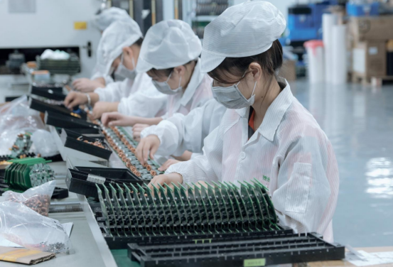
After solder paste application, components are placed onto the PCB. This can be done automatically with pick-and-place machines or manually for small-scale or specialized assemblies.
Pick-and-place machines position components with high precision, even for fine-pitch ICs, tiny resistors, and capacitors. Manual placement is typically used for large components or prototypes. Accuracy is critical: misaligned components can result in open circuits, shorts, or tombstoning during soldering.
For example, placing a 0402 resistor correctly ensures that both ends of the component connect to the solder paste evenly, preventing defects after reflow.
Reflow Soldering
Reflow soldering melts the solder paste to create strong electrical and mechanical connections. This process follows a temperature profile with several stages:
1. Preheat: Gradually warms the PCB to avoid thermal shock.
2. Soak: Stabilizes the temperature and activates flux in the solder paste.
3. Reflow: Peaks at the solder’s melting point, allowing it to bond components.
4. Cooling: Gradually cools the PCB to solidify solder joints.
Lead-free solder requires a higher reflow temperature than leaded solder, which can affect sensitive components. Leaded solder is easier to work with but is less environmentally friendly. Choosing the right solder type depends on regulatory standards and product requirements.
Post-Reflow Inspection
Once soldering is complete, inspection ensures the assembly meets quality standards. Automated Optical Inspection (AOI) uses cameras to detect defects like misalignment, missing components, and solder bridges. Manual visual checks are also used for critical areas or complex boards.
Common defects in SMT assembly include:
Tombstoning: A component standing on one end due to uneven solder.
Solder bridges: Unintended connections between adjacent pads.
Misalignment: Components not seated correctly on the pads.
Early detection of these defects reduces rework costs and improves overall reliability.
Through-Hole Technology (THT) Assembly
Component Insertion
Through-Hole Technology (THT) assembly involves inserting component leads through pre-drilled holes in the PCB. The process begins by identifying the correct holes for each component based on the assembly drawing. Leads are inserted carefully, and for stability, they are sometimes bent slightly on the opposite side of the board to hold components in place during soldering.
THT insertion can be done manually for prototypes or low-volume boards, or automated using insertion machines for high-volume production. Automated machines increase speed and accuracy, while manual insertion allows for flexibility with large or unusual components. For example, a large electrolytic capacitor may require manual placement due to its size.
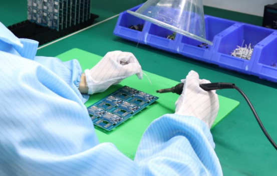
Soldering Techniques
Once components are inserted, soldering secures them electrically and mechanically. There are two main techniques:
1. Wave Soldering:
The PCB passes over a wave of molten solder that attaches all component leads at once.
Advantages: Fast, consistent, suitable for high-volume production.
Limitations: Not ideal for boards with many SMT components or very fine-pitch leads.
2. Hand Soldering:
Involves using a soldering iron, solder wire, and flux to join leads individually.
Tips for beginners: Use proper temperature settings, clean the tip regularly, and apply just enough solder to form a reliable joint.
Hand soldering is often used for rework, prototypes, or components that cannot go through wave soldering.
Inspection and Testing
After soldering, inspection and testing ensure the THT assembly is reliable. Key issues to look for include:
Cold joints: Poorly formed solder connections that may cause intermittent failures.
Shorts: Unintended connections between adjacent leads or pads.
Misaligned components: Leads not properly inserted or bent incorrectly.
Typical THT defects can be detected visually or with basic continuity testing using a multimeter. For example, a resistor whose leads are not fully soldered may appear connected but fail under electrical testing. Early identification of defects reduces rework costs and improves the PCB’s long-term reliability.
Post-Assembly Processes
Cleaning and Residue Removal
After assembly, PCBs often have solder flux residues, dust, or oils that can affect performance or reliability. Cleaning methods vary depending on the type of flux and assembly process:
Chemical cleaning: Uses solvents to remove flux residues from the board surface. Effective for rosin-based fluxes but requires proper ventilation.
Ultrasonic cleaning: Submerges the PCB in a liquid bath while ultrasonic waves remove residues from hard-to-reach areas. Ideal for complex assemblies with dense component placement.
No-clean flux: Some modern solder pastes leave minimal residue, eliminating the need for cleaning in many cases. However, visual inspection is still recommended.
Proper cleaning improves solder joint reliability and prevents corrosion over time. For example, a board with leftover flux on high-voltage circuits may develop leakage currents if not cleaned.
Testing and Quality Assurance
Testing ensures that the assembled PCB functions correctly and meets quality standards. Common testing methods include:
Functional testing: Simulates the PCB’s real-world operation to verify that circuits and components work as intended.
In-circuit testing (ICT): Checks individual components and connections using probes, identifying shorts, opens, or incorrect values.
X-ray inspection: Detects hidden defects like solder voids, BGA misalignment, or internal cracks.
Each method has trade-offs. Functional testing is cost-effective for simple boards but may miss hidden defects. ICT is more thorough but requires specialized equipment. X-ray inspection is highly reliable but expensive, often reserved for critical applications.
Rework and Repair
Even with careful assembly, defects can occur. Common issues requiring rework include solder bridges, missing components, cold joints, or misaligned parts.
Step-by-step repair techniques for beginners:
Identify the defect using visual inspection or testing tools.
For solder bridges, carefully remove excess solder with a solder wick or desoldering pump.
Replace missing or damaged components using the correct soldering method (SMT or THT).
Reinspect the repaired area to ensure proper connection and alignment.
For example, a misaligned resistor can be carefully lifted, repositioned, and soldered without damaging surrounding traces. Proper rework improves PCB yield and prevents future failures.
Best Practices for Beginners
Handling and Storage of Components
Proper handling and storage of components are critical to prevent damage and ensure reliable PCB assembly. Electrostatic discharge (ESD) precautions should always be followed, including using anti-static mats, wrist straps, and ESD-safe tools.
Components should be stored in original packaging or moisture-proof containers to protect against humidity, dust, and mechanical damage. For example, moisture-sensitive devices like certain ICs may require sealed bags with desiccant packs to prevent soldering defects such as popcorn cracking during reflow.
A controlled storage environment with stable temperature and low humidity helps maintain component integrity and extends shelf life. Beginners should label and organize components clearly to avoid mix-ups during assembly.
Process Optimization Tips
Optimizing the assembly process improves efficiency and reduces errors. Beginners can follow these tips:
Follow Standard Operating Procedures (SOPs): Clear step-by-step instructions reduce mistakes and ensure consistency.
Minimize handling: Every unnecessary touch increases the risk of ESD damage or contamination.
Inspect regularly: Early detection of misaligned components or solder defects prevents costly rework.
Batch work effectively: Grouping similar tasks (like soldering or inspection) improves workflow and efficiency.
For example, pre-sorting resistors and capacitors by value before starting assembly saves time and reduces errors during placement.
Safety Guidelines
Safety is essential during PCB assembly. Key precautions include:
Soldering safety: Use a properly grounded soldering iron, avoid touching the hot tip, and keep a fire extinguisher nearby.
Ventilation: Fumes from solder flux can be harmful; work in a well-ventilated area or use a fume extractor.
Personal Protective Equipment (PPE): Safety glasses, gloves, and protective clothing reduce exposure to heat, chemicals, and sharp leads.
For example, wearing safety glasses prevents eye injury from solder splashes, while proper ventilation protects respiratory health during extended soldering sessions.
Conclusion
The PCB assembly process combines Surface Mount Technology (SMT) and Through-Hole Technology (THT) to create fully functional electronic circuits. SMT involves applying solder paste, placing components precisely on the board, and using reflow soldering to form reliable connections, while THT focuses on inserting component leads through drilled holes and securing them with wave or hand soldering. Together, these methods ensure that PCBs can support a wide range of devices, from consumer electronics to industrial systems, providing both performance and reliability.
For beginners, mastering PCB assembly is a gradual process that benefits from careful practice, attention to soldering techniques, and adherence to safety measures such as ESD precautions and proper ventilation. Using hands-on kits, tutorials, and manufacturer guides helps reduce mistakes and build confidence. Experimenting safely allows learners to refine skills and gradually achieve professional-quality results.
Manufacturers like PCBMASTER support this learning and production journey by offering high-quality PCBs and assembly services that cater to both educational projects and professional applications. With reliable boards and accessible guidance, anyone—from beginners to experienced engineers—can turn electronic designs into functional, high-performance circuits.
FAQs
What is the difference between SMT and THT assembly?
Surface Mount Technology (SMT) involves placing components directly on the surface of the PCB. Components are usually small, lightweight, and mounted using solder paste and reflow soldering. SMT is ideal for high-density boards and automated production.
Through-Hole Technology (THT) involves inserting component leads through pre-drilled holes in the PCB and soldering them on the opposite side. THT provides stronger mechanical connections and is often used for large components or boards that require higher durability.
In short, SMT is faster, more compact, and suited for automation, while THT offers mechanical strength and is easier for manual assembly.
How can beginners avoid common soldering defects?
Beginners can reduce defects by following a few key practices:
Use proper soldering techniques: Apply the right amount of solder and heat, avoiding cold joints or solder bridges.
Keep components clean: Ensure boards and leads are free of dust or oxidation.
Handle parts carefully: Follow ESD precautions and avoid touching soldered areas.
Inspect work: Check joints visually or with magnification before moving to the next step.
Common defects like cold joints, misaligned components, or tombstoning can often be prevented with patience, proper tools, and careful preparation.
What tools are essential for PCB assembly at home or in a lab?
Basic tools for PCB assembly include:
Soldering iron with adjustable temperature
Solder wire and flux
Tweezers for precise component placement
Magnification tools like a loupe or microscope
Multimeter for basic electrical testing
Anti-static tools such as wrist straps and mats
Optional but useful tools for beginners: solder wick, desoldering pump, and a small fume extractor for ventilation.
These tools allow both SMT and THT assembly, inspection, and testing in a home or lab setting.
How do manufacturers test PCB assemblies for reliability?
Manufacturers use multiple testing methods to ensure PCBs function correctly and are reliable:
Functional testing: Simulates the real operation of the device to check overall performance.
In-Circuit Testing (ICT): Tests individual components, connections, and detects shorts or open circuits.
Automated Optical Inspection (AOI): Uses cameras to detect misaligned or missing components.
X-ray inspection: Reveals hidden defects, such as BGA solder voids or internal cracks.
The combination of these tests helps catch defects early and ensures the PCB performs reliably under normal operating conditions.
Can the PCB assembly process be automated completely, and what are the limitations?
While many PCB assembly steps can be automated—especially SMT placement, reflow soldering, and inspection—complete automation has limitations:
THT insertion often requires manual intervention for unusual or large components.
Complex prototypes or small batches may not be cost-effective to automate.
Rework and repair almost always require human expertise for precision and problem-solving.
In practice, automation is highly efficient for high-volume production, but skilled operators remain essential for quality control, troubleshooting, and specialized tasks.

