


What Is PCB Assembly? Understanding Its Role in Electronics Manufacturing
Have you ever wondered how the tiny parts inside your phone or TV are connected together so they can work? That is where PCB assembly comes in.
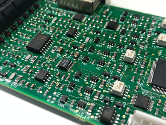
PCB assembly is the process of putting all the little electronic parts onto a flat green board, called a PCB, so they can talk to each other and make your device do its job. Without this process, no modern electronics could work — not your phone, computer, car, or even your washing machine.
In this article, we will explore what PCB assembly really means, how it is done step by step, and why it is so important for making the gadgets we use every day.
What Is PCB Assembly?
PCB assembly is like building the “brain” of an electronic device. First, we start with a bare board — a flat piece made of fiberglass with thin copper lines on it. These copper lines are like tiny highways for electricity. On its own, this board does nothing.
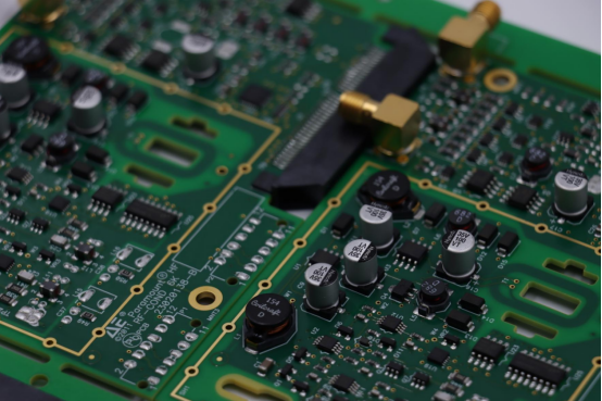
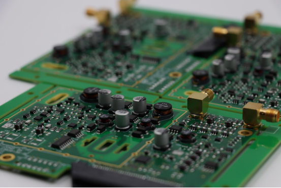
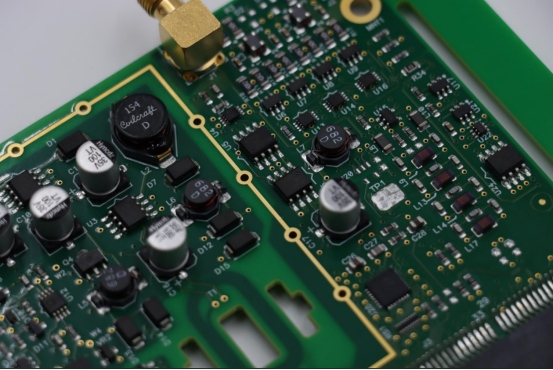
Next, we take electronic components — such as tiny chips, resistors, capacitors, LEDs, and connectors — and put them in their correct places on the board. Each part has a job: some store energy, some control signals, and some connect to other devices.
Once everything is in place, we solder the parts. Solder is a metal that melts when heated and hardens when it cools. It works like glue, but for electricity. It holds the parts tightly and lets electricity flow through them so the whole circuit can work.
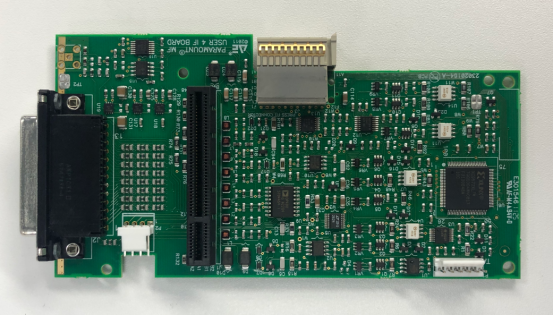
When this process is complete, the board is no longer empty — it becomes a PCBA, a working circuit ready to be put inside a phone, TV, computer, or car system.
Common Terms You Should Know
To avoid confusion, here are some important words:
· PCB (Printed Circuit Board) – Just the empty board with copper tracks, no parts attached. Think of it like the frame of a house before furniture is added.
· PCBA (Printed Circuit Board Assembly) – The finished board with all the parts soldered in place. Like a house with furniture, lights, and appliances installed — ready to live in.
· SMT (Surface Mount Technology) – A way of attaching very small components directly on top of the copper pads. This is the most common method because it is fast and works for modern mini devices like smartphones.
· THT (Through-Hole Technology) – A method where parts have metal legs that go through holes in the board and get soldered on the back side. This makes the parts very strong, which is good for heavy or high-power components.
Why We Do PCB Assembly
The purpose of PCB assembly is to make the circuit board actually work. Before assembly, the board is just like an empty shell. After assembly, it becomes the “heart” of your device, sending signals, turning things on or off, and making the product function as designed.
For example:
· Inside a TV, the assembled PCB manages the picture and sound.
· For cars, it takes charge of the engine, lights, and sensors.
· In a washing machine, it decides when the drum should start or stop spinning.
Without PCB assembly, none of these machines could do anything.
Main Steps of PCB Assembly
Making a circuit board into a working PCBA is not just one step — it is a carefully planned process. Think of it as building a car: first you design it, then gather all the parts, then put them together, test it, and finally deliver it. Here’s what really happens, step by step:
1. Design and BOM Preparation
Everything starts with a design. Engineers first create a schematic diagram, which is like a wiring plan showing how all the components will connect. Then they make Gerber files, which are digital blueprints used by the factory. Gerber files tell the machines where the copper tracks go, where to drill holes, and where each component should sit.
Next comes the BOM (Bill of Materials). This is a very detailed list of every single component: part numbers, quantity, size, value, and the exact location on the board (called a reference designator, like R1 or C5). A good BOM is critical — if even one part number is wrong, the whole product could fail or be delayed.
Factories often check the BOM carefully before production. If some parts are hard to find, they may suggest replacements so the project can stay on schedule.
2. Solder Paste Printing
Once the bare boards arrive at the factory, the first step on the production line is solder paste printing. A metal stencil, which looks like a thin mask with small holes, is placed over the board.
A machine spreads solder paste across the stencil, and the paste only goes through the holes, landing exactly on the pads where components will sit. This process must be very precise — too much paste can cause short circuits, and too little can cause weak joints.
After this step, each pad has a tiny amount of gray paste on it, ready to “catch” a component.
3. Pick-and-Place (SMT Component Mounting)
The board then moves to a pick-and-place machine. This machine uses vacuum nozzles to pick tiny components from reels or trays and place them on the board, one by one, very quickly and accurately.
Modern machines can place tens of thousands of components per hour and have cameras to make sure each part is perfectly aligned. Even the smallest chips — smaller than a grain of rice — are placed correctly.
For very sensitive parts like microcontrollers, the machine places them carefully so the pins line up exactly with the pads.
4. Reflow Soldering
When all components are placed, the board goes into a reflow oven. This oven has several zones:
· Preheat zone slowly warms the board.
· Soak zone keeps the temperature stable so the solder paste spreads evenly.
· Reflow zone gets hot enough to melt the solder (around 220°C for lead-free solder).
· Cooling zone cools the board down so the solder becomes solid and strong.
This step is very important — if the heating profile is wrong, solder joints might be weak, or components could be damaged.
5. THT Insertion and Wave Soldering (If Required)
Some boards also use THT (Through-Hole Technology) for big components like transformers, connectors, or heavy switches.
Workers or robotic arms insert these parts into the holes by hand or machine. Then the board passes over a machine with a big wave of hot liquid solder. The wave touches the bottom of the board and solders all the pins at once.
This process makes very strong connections that can handle stress, which is why THT is still used for parts that must be mechanically strong.
6. Inspection and Testing
Quality control is critical. After soldering, the board is checked at several levels:
· AOI (Automated Optical Inspection): Cameras look for missing parts, wrong parts, or crooked parts.
· X-Ray Inspection: Used for hidden joints, like under BGAs (Ball Grid Arrays). This finds solder bridges or empty joints that you cannot see with normal cameras.
· In-Circuit Test (ICT): Special probes touch test points on the board to check if every connection is correct.
· Functional Test: The board is powered on and tested in real working conditions to make sure it behaves exactly as designed.
If a problem is found, the board goes to a rework station where skilled technicians fix it.
7. Cleaning and Final Packaging
After testing, boards may still have flux residue or tiny particles on them. They go through a special cleaning machine that sprays them with cleaning solution and dries them. Clean boards are less likely to corrode and are more reliable.
Finally, the boards are carefully packed with anti-static bags, foam, or trays to prevent damage during shipping. Each package is labeled with part number, lot number, and date so it can be tracked later if needed.
Common Methods and Technologies in PCB Assembly
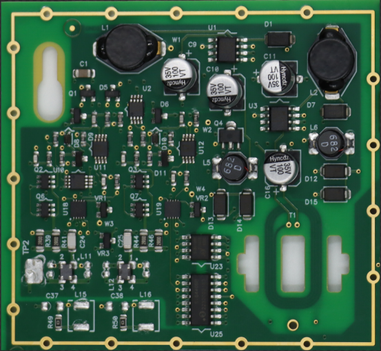
PCB assembly can be done in different ways depending on the components, board design, and device requirements. The three main methods are SMT, THT, and Mixed Assembly. Each method has its own process, advantages, and disadvantages.
1. SMT (Surface Mount Technology)
SMT is a method where components are placed directly on the surface of the PCB. These parts do not have long metal legs; instead, they sit on small copper pads. A pick-and-place machine positions each component precisely, and then the board goes through a reflow oven, where solder paste melts and forms a solid electrical and mechanical connection.
Advantages:
SMT allows very high component density, meaning more parts can fit on a small board. This is ideal for compact devices like smartphones, tablets, and laptops. The process is highly automated, making it fast and suitable for mass production.
Disadvantages:
Components are very small and delicate, so repairing or replacing them can be difficult. SMT is not suitable for heavy components that need strong mechanical support.
Example / Reference:
Most modern consumer electronics, like smartphones and networking devices, rely heavily on SMT to achieve high performance in a small size.
2. THT (Through-Hole Technology)
THT is a method where components have metal leads that go through holes in the PCB. After insertion, the leads are soldered on the opposite side of the board. This can be done manually or with wave soldering machines. The result is a very strong mechanical and electrical connection.
Advantages:
THT creates strong and reliable connections, making it suitable for heavy components or parts that experience vibration, stress, or high heat. It is commonly used for connectors, transformers, and large LEDs.
Disadvantages:
THT assembly is slower and often requires manual insertion of parts, increasing cost. It also cannot achieve the same high density as SMT, so it is less suitable for small consumer devices.
Example / Reference:
Automotive control boards and industrial machinery often use THT for power components and connectors that need high mechanical strength.
3. Mixed Assembly (SMT + THT)
Mixed assembly combines SMT and THT. First, SMT components are placed and soldered on the surface of the board. Then, THT components are inserted and soldered using wave soldering or selective soldering. This method allows a board to include both tiny, high-density parts and large, strong components.
Advantages:
Mixed assembly offers flexibility, allowing boards to meet both high-density and high-strength requirements. It is ideal for complex electronics that include both delicate sensors and heavy power devices.
Disadvantages:
The process is more complex and must be carefully sequenced to avoid damaging SMT parts during THT soldering. It can also increase production cost due to the additional steps.
Example / Reference:
Automotive electronics, medical devices, and industrial machinery often use mixed assembly to combine small SMT sensors with large THT connectors or power components.
The Role and Value of PCB Assembly in Electronics Manufacturing
PCB assembly is not just putting parts on a board — it is a critical step that affects how fast a product can be made, how well it works, and how reliable it will be. Each stage of assembly has a direct impact on the final product.
1. Shortening Product Time-to-Market
Automated PCB assembly machines can place thousands of tiny components in just a few hours. By combining fast SMT processes, accurate pick-and-place machines, and efficient reflow ovens, manufacturers can produce complex boards much faster than manual assembly.
The faster a company can assemble and test its boards, the sooner the product reaches customers. For example, a smartphone manufacturer can release a new model quickly before competitors, capturing more sales and market attention.
Example / Reference: Companies like Apple and Samsung rely on highly automated PCB assembly lines to launch new phones every year. Even a small delay in PCB assembly can push the product launch back by weeks.
2. Improving Reliability and Consistency
Automated PCB assembly ensures that every component is placed precisely, and solder joints are strong. Inspection systems like AOI (Automated Optical Inspection), X-ray, and functional testing catch mistakes before the boards leave the factory.
Reliable assembly reduces product failures. Consistency means each device works the same way, whether it’s the first unit or the thousandth. This is especially critical for safety-sensitive products like car electronics, pacemakers, or industrial machines.
Example / Reference: Automotive ECUs (engine control units) use highly reliable PCB assemblies. Even a single bad solder joint could cause engine failure. Consistent assembly ensures each car works safely.
3. Supporting High-Density, Small, and Complex Designs
SMT and mixed assembly allow hundreds or thousands of tiny components to fit onto a small PCB. Engineers can design multi-layer boards with complex circuits that would not fit using older through-hole methods alone.
This enables miniaturized electronics without losing performance. Devices like smartwatches, drones, and wearable health monitors rely on high-density PCB assemblies to include sensors, processors, and communication modules in a tiny space.
Example / Reference: A smartwatch PCB may have over 1,000 SMT components in a space smaller than a coin. Without precise assembly, it would be impossible to fit so much functionality into such a small device.
4. Impacting Production Costs and Supply Chain Efficiency
Efficient PCB assembly reduces errors, rework, and scrap, which lowers material waste. Automated processes reduce labor costs. Proper BOM planning and coordination with suppliers ensure that all components arrive on time.
Lower production costs and smooth supply chains allow companies to deliver high-quality products on schedule while remaining competitive. Delays or mistakes in PCB assembly can increase costs and affect the entire product line.
Example / Reference: In laptop manufacturing, a single missing or misaligned component on the PCB can halt the assembly of hundreds of units. Efficient assembly and supply chain management prevent such costly delays.
Common Challenges and Solutions in PCB Assembly
PCB assembly is a complex process, and even small mistakes can cause serious problems. Understanding these challenges and how to solve them is essential for making reliable electronic devices.
1. Quality Control: Solder Defects, Component Misalignment, and Cold Solder Joints
One of the biggest challenges in PCB assembly is quality control. Solder defects, component misalignment, and cold solder joints are common problems. A solder defect occurs when the metal does not properly connect a component to the board, making the connection weak. Components may also be placed slightly off their pads, which can prevent the circuit from working. Cold solder joints look normal but do not conduct electricity properly, often caused by incorrect heating during soldering.
These issues usually happen because of improper solder paste application, miscalibrated pick-and-place machines, or uneven heating in the reflow oven. If left unchecked, they can cause devices to fail immediately or after some time, and even a single defective board can ruin a whole batch.
How manufacturers solve this includes automated inspections like AOI (Automated Optical Inspection) and X-ray machines to check hidden joints. If defects are found, skilled technicians fix solder joints or reposition components. Regular calibration and preventive maintenance of machines also help maintain consistent quality. For example, in automotive electronics, a misaligned sensor can cause critical engine or safety system failures, so inspection and rework are essential to ensure reliability.
2. Material Management: BOM Errors and Component Shortages
Another major challenge is material management. Sometimes mistakes in the Bill of Materials (BOM) can cause the wrong parts to be used, or the correct parts may not be available when needed. These issues happen due to design errors, last-minute changes, or global supply chain delays.
The impact is significant. Production can stop completely if a key component is missing, leading to delays and extra costs. Using the wrong part can also result in product failure after shipment.
To address these challenges, manufacturers carefully review the BOM before production, double-check part numbers and quantities, and maintain backup suppliers and buffer stock. Clear communication about design changes is also critical to avoid mistakes. For instance, laptop assembly lines can halt if a single memory chip is unavailable, so proper material management ensures smooth production.
3. Process Optimization: Improving Yield and Reducing Scrap
Even with good machines and materials, some boards may fail during production. High scrap rates can increase costs and slow down manufacturing. Common causes include incorrect machine settings, uneven solder paste, inconsistent reflow oven temperatures, or insufficient operator training.
Improving the process involves continuously monitoring machine settings, controlling solder paste volume, and maintaining consistent oven profiles. Operators are trained to handle boards carefully and follow standard procedures. Feedback from inspection results is used to identify problem areas and optimize the process. For example, smartphone factories use statistical process control to monitor defects. By adjusting solder paste volumes and oven settings, they can reduce defective boards to less than 1% per run, saving significant cost and time.
Conclusion
PCB assembly is the process of turning a bare circuit board into a fully working electronic device. We have seen how it involves careful planning, precise placement of components, soldering, inspection, and testing. Each step is important to make sure the final product works reliably and consistently.
In modern electronics, PCB assembly is at the heart of every device, from smartphones and laptops to cars and medical machines. It enables small, complex, and high-performance designs that would be impossible without precise assembly.
For companies, choosing a professional PCB assembly service, like the expert solutions provided by PCBMASTER, can make a real difference. Using experienced partners ensures higher quality, fewer defects, faster production, and stronger competitiveness in the market. Investing in professional PCB assembly is not just about making a product—it’s about building reliability, efficiency, and trust in every device.
FAQs
1. How do manufacturers handle extremely small components in PCB assembly?
Tiny components, sometimes smaller than a grain of rice, are handled using specialized machines called pick-and-place machines. These machines use vacuum nozzles to pick up each small component and place it precisely on the PCB. After placement, the board goes through a reflow oven to melt the solder paste and make a strong electrical connection. Manual handling of such small parts is nearly impossible, so automation ensures accuracy, speed, and consistency, especially for devices like smartphones, tablets, and wearable electronics.
2. Why is testing so important after PCB assembly?
Testing is crucial because even a small mistake in assembly can cause a device to fail. Manufacturers use visual inspection, automated optical inspection (AOI), X-ray inspection, and functional testing. Visual inspection can catch obvious problems like missing parts or misalignment. AOI and X-ray can detect hidden solder defects, especially under complex chips like BGAs. Functional testing ensures the board actually works as intended, powering up the circuit and checking all functions. Testing prevents defective products from reaching customers, improving reliability and safety.
3. Can PCB assembly affect the overall design of an electronic product?
Yes, PCB assembly directly affects the size, performance, and complexity of a product. For example, SMT allows very small components to be placed close together, making the board compact and enabling smaller devices like smartwatches and drones. THT is used for strong, heavy components like connectors and transformers. Choosing the right assembly method influences whether a product can be miniaturized, how reliable it will be, and how quickly it can be manufactured. Careful planning of PCB assembly is therefore essential for both design and production.
4. How does the choice of PCB material affect assembly and device performance?
The material of a PCB affects how easy it is to assemble and how well the device performs. Common PCB materials include FR-4, CEM-1, and flexible substrates for FPCs. FR-4 is strong, stable, and works well for most electronics, making it easy to solder components. Flexible PCBs can bend, which is useful for wearable devices or foldable phones, but they require careful handling during assembly to avoid damaging traces or pads. The right material ensures good soldering, electrical performance, and long-term reliability. Choosing the wrong material can cause solder failures, overheating, or reduced device life.
5. How does PCB assembly influence production cost and supply chain efficiency?
PCB assembly can significantly impact production cost and supply chain management. Automated processes like SMT reduce labor costs and speed up production, but the machines and setup require investment. Errors in assembly can cause scrap, which wastes materials and increases cost. Efficient BOM planning, timely ordering of components, and reliable suppliers prevent delays. For example, if a critical part is out of stock, the entire production line may stop, causing financial loss. Well-organized PCB assembly ensures faster manufacturing, less waste, and smoother supply chains, ultimately saving money and keeping products competitive in the market.

