What Is Bumping? The Key Technology Behind Advanced Packaging
In advanced semiconductor packaging, every micron matters. As devices push for higher speed, lower power, and tighter integration, the simple act of connecting a chip to the outside world becomes a decisive factor in overall performance. Hidden beneath today’s AI processors, smartphone SoCs, automotive controllers, and high-density modules is a quiet enabler that makes this progress possible: the microscopic metal bumps that form the chip’s first layer of electrical contact.
These bumps may look insignificant, but they determine how fast signals travel, how much heat can be dissipated, and how densely functions can be integrated. From enabling ultra-fine I/O layouts to supporting the shift toward 2.5D and 3D architectures, bumping technology has evolved into one of the key foundations of modern packaging innovation.
What Is Bumping Technology?
Definition of Bumping
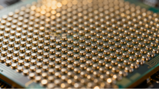
Bumping is a core interconnect process used to create electrical connections between a semiconductor chip and the outside world. Instead of using long wires, bumping forms tiny metal protrusions—called bumps—directly on the surface of the die. Each bump acts as an individual contact point, enabling a chip to communicate with a substrate, another chip, or a package.
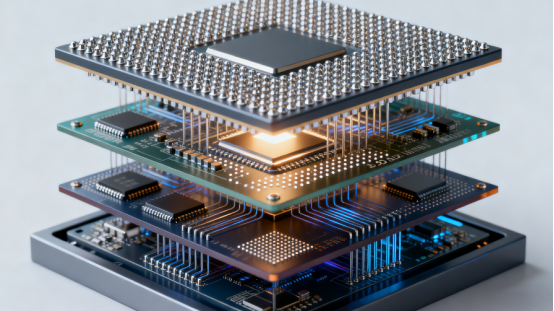
A bump provides a short, direct, and highly conductive path. This makes it essential for advanced packaging formats such as Flip Chip, Wafer Level Packaging (WLP), Fan-out and Fan-in, Chip-Scale Packages (CSP), 2.5D and 3D integration, and System-in-Package (SiP). These architectures depend on dense, high-performance interconnects, and bumping enables the required number of I/O connections within limited space.
Because the bumps are formed at the wafer level, the process supports high-volume production and consistent electrical performance across all devices on the wafer.
How Bumping Differs from Traditional Wire Bonding
Traditional packaging relies on wire bonding. In this method, a thin metal wire (often gold, aluminum, or copper) connects the chip’s bond pads to the lead frame or substrate. While widely used, wire bonding creates long electrical paths that introduce resistance, inductance, and parasitic effects. These parasitics limit signal speed, degrade high-frequency performance, and increase power loss.
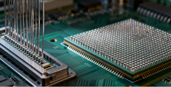
Bumping enables Flip Chip interconnects, where the die is flipped face-down and the bumps directly land on the substrate. This configuration dramatically shortens the interconnect length—from millimeters in wire bonding to microns in bumping. The shorter the path, the lower the inductance and resistance. As a result, Flip Chip devices offer better signal integrity, higher bandwidth, and improved performance in high-speed applications.
For example:
A wire bond may be several millimeters long, creating significant loop inductance.
A bump connection is only tens of microns tall, reducing inductance by an order of magnitude.
This shorter path reduces voltage drop, improves timing margins, and supports multi-GHz signal transmission.
In simple terms: wire bonding works, but bumping works faster, cleaner, and at far higher I/O density, making it the preferred choice for modern high-performance and miniaturized semiconductor devices.
The Importance and Future Direction of Bumping Technology
Bumping as a Core Enabler of Advanced Packaging
Bumping plays a foundational role in the evolution of advanced semiconductor packaging. It is a required interconnect method for Flip Chip, fan-out packaging, fan-in packaging, and 2.5D/3D integration, where chips must support high-density electrical connections within extremely limited space. Without bumping, these architectures cannot achieve the short interconnects and dense I/O layouts that define modern high-performance systems.
A key reason bumping is essential is its ability to increase I/O density. As chips integrate more functions—AI acceleration, memory stacking, RF modules, power management—they require thousands of individual contact points. Bumping enables these connections to be placed closely together, directly on the die surface. This contributes to higher packaging density, better electrical performance, and greater system integration. Many cutting-edge devices, from AI processors to smartphone application processors, depend on this capability to achieve their performance targets.
In short, bumping is not just an interconnect method—it is a core infrastructure technology that allows advanced packaging to scale.
Shrinking Bump Pitch and Rising Manufacturing Challenges
As demand for higher performance and smaller form factors increases, bump pitch—the center-to-center spacing between bumps—continues to shrink. A smaller pitch enables more bumps per unit area, which directly translates to higher I/O count, higher bandwidth, and thinner packages. For example, reducing pitch from 100 µm to 40 µm can more than double the available interconnects, enabling finer redistribution layers and more complex system integration.
However, shrinking the pitch also makes manufacturing significantly more difficult. Each reduction introduces new challenges, including:
More precise lithography masks, required to define much smaller bump sites
Tighter electroplating control, ensuring consistent bump height and diameter
Accurate solder volume management, as even slight deviations can cause bridging, voids, or alignment failures
These challenges become especially severe at ultra-fine pitches used in 3D stacking and chip-to-chip hybrid bonding.
As the industry moves toward sub-20 µm bumps and heterogeneous 3D architectures, improvements in materials, plating chemistry, and wafer-level processing will become critical. The trend is clear: higher density requires finer bumps, and finer bumps demand next-generation manufacturing precision.
Common Types of Bumps and How They Compare
Solder Bumps
A solder bump is formed using a small sphere of tin-based alloy, typically tin or tin–silver. This structure melts during reflow and forms the electrical and mechanical connection between the chip and substrate. Solder bumps are one of the most mature interconnect technologies in semiconductor packaging.
Their main advantage is low cost and a highly established manufacturing ecosystem, making them ideal for high-volume products. However, solder bumps have limitations when the required bump pitch becomes very small. As the pitch shrinks, the solder volume becomes harder to control, and the risk of bridging or voids increases. Because solder bumps rely on molten solder to form the joint, they also show weaker performance in high-frequency or high-speed applications, where parasitic inductance and signal loss become critical.
Solder bumps are widely used in general-purpose ASICs, low-to-medium speed logic devices, consumer electronics ICs, and cost-sensitive packages where extreme density is not required.
Cu Pillar Bumps
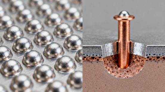
A Cu pillar bump consists of a solid copper column topped with a small solder cap, typically separated by a nickel barrier layer. The copper pillar provides structural strength and a highly conductive path, while the solder cap ensures reliable bonding during reflow. This composite structure allows Cu pillars to outperform solder bumps in several ways.
The first advantage is superior reliability, particularly in electromigration resistance. Copper is significantly more stable under high current density, making these bumps ideal for power-hungry and high-speed chips. Second, Cu pillar bumps can be produced at a much smaller pitch, enabling very high I/O density needed for modern advanced packaging. Third, copper’s thermal conductivity improves heat dissipation, which is essential for devices with high switching activity.
Long-term tests often show dramatic differences: under identical thermal and current conditions, copper pillar bumps can survive 8,000 hours of stress testing without the failures observed in tin-silver bumps. This reliability makes them the preferred solution for high-speed processors, AI accelerators, baseband chips, GPUs, application processors, and automotive-grade devices.
Solder Bumps vs. Cu Pillar Bumps: Key Differences
When comparing solder bumps with copper pillar bumps, several practical differences emerge:
Pitch Range:
Solder bumps support moderate pitch sizes.
Cu pillars enable finer pitches suitable for high-density packaging.
Reliability:
Solder bumps are adequate for standard applications.
Cu pillars offer far higher electromigration resistance and long-term stability.
Thermal Performance:
Solder bumps have limited heat conduction.
Copper pillars provide superior thermal paths for heat dissipation.
Cost:
Solder bumps are lower cost and widely accessible.
Cu pillars are more expensive due to additional layers and tighter process control.
Typical Use Cases:
Solder bumps: mainstream ASICs, low-speed ICs, cost-driven products.
Cu pillars: AI/HPC chips, GPUs, RF/baseband ICs, automotive electronics, and high-speed logic.
In summary, solder bumps maximize cost efficiency, while Cu pillar bumps maximize performance and reliability. The choice depends on the application’s speed, density, and thermal requirements.
The Role and Structure of UBM (Under Bump Metallization)
What UBM Is and Why It Is Essential
Under Bump Metallization (UBM) is a multilayer metal stack formed between the chip’s pad and the bump. It serves as the foundation that allows a solder bump or copper pillar bump to attach securely to the die. Without UBM, the bump would not bond properly to the silicon pad, leading to weak joints and early failure.
UBM performs three essential functions. First, it provides mechanical adhesion, ensuring the bump stays firmly connected to the chip surface. Second, it offers good electrical contact by forming a conductive interface between the pad and the bump. Third, UBM prevents metal diffusion, electromigration, and interfacial brittleness, all of which could compromise long-term reliability. These protective roles are especially important in high-current or high-temperature environments, where unprotected interfaces degrade rapidly.
In short, UBM is the engineered “glue layer” that makes bumping possible while ensuring durability, conductivity, and stability over the device’s lifetime.
The Typical Three-Layer Structure of UBM
A standard UBM stack consists of three functional layers, applied from the chip side outward:
Adhesion Layer (e.g., Titanium, Chromium)
This inner layer bonds directly to the aluminum or copper pad on the chip. Its primary role is to anchor the metallization stack securely to the surface.
Current-Carrying Layer (e.g., Copper)
The middle layer provides a low-resistance path for electrical current and acts as the main structural body. It determines how well the interconnect handles high current density.
Wetting Layer (e.g., Nickel, Gold)
The outer layer promotes proper wetting during solder reflow or copper plating. It also acts as a barrier to stop unwanted diffusion between the solder, copper pillar, and underlying layers.
Together, these layers create a stable interface that supports both mechanical bonding and electrical reliability.
How UBM Is Manufactured
UBM layers are typically deposited using two wafer-level methods:
Sputtering (Physical Vapor Deposition)
Sputtering is used to deposit thin, uniform adhesion and seed layers across the wafer. It allows excellent control over thickness and composition, which is critical for fine-pitch bumping.
Electroplating (Electrochemical Deposition)
After sputtering a seed layer, electroplating builds up thicker copper or nickel layers required for current carrying and wetting functions. Electroplating is efficient, scalable, and well-suited for high-volume manufacturing.
These processes work together to form a precisely engineered UBM stack tailored to the bump type and the package’s performance requirements.
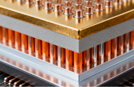
Three Primary Methods for Solder Bump Fabrication
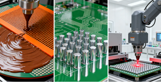
Stencil Printing (Printing Method)
Stencil printing is one of the simplest ways to create solder bumps. In this process, solder paste is deposited onto the wafer through a precision stencil, aligning with the underlying UBM pads. After printing, the wafer undergoes a reflow process, during which the solder melts and forms spherical bumps.
Advantages:
Low cost and straightforward process
Minimal equipment requirements, making it suitable for smaller manufacturing lines
Limitations:
Difficulty achieving ultra-fine pitch (<100 µm) due to solder spreading and stencil resolution
Risk of voids or uneven solder volume, which can affect reliability
Typical Applications:
Cost-sensitive devices
Packages with relatively large bump pitch, such as mainstream consumer ASICs or low-speed ICs
Electroplating Bumping (Plating Method)
Electroplating is currently the most widely used method for creating solder bumps and can also be applied for Cu pillar bumps. This method builds up bumps layer by layer on top of the UBM, providing precise control over bump height and shape.
Advantages:
High production yield and uniformity
Suitable for small pitch and high-density interconnects
Excellent control over bump morphology
Step-by-Step Process:
1. Deposit UBM on the wafer
2. Apply photoresist and pattern the bump locations using lithography
3. Electroplate solder or copper onto the exposed UBM areas
4. Strip the photoresist
5. Perform reflow to form rounded, reliable bumps
This method is ideal for advanced packaging applications that require high-density I/O and fine-pitch interconnects.
Ball Drop / Ball Placement (Pre-formed Solder Ball Method)
Ball drop or ball placement involves placing pre-formed solder balls onto the wafer at designated UBM sites using automated equipment. After placement, the wafer is reflowed so the balls bond to the underlying pads.
Advantages:
High throughput, making it suitable for large-scale production
Stable process with high yield for appropriately sized bumps
Limitations:
Potential for defects such as missing balls, double balls, or misalignment
Not suitable for extremely small diameter bumps due to placement accuracy limits
Typical Applications:
Image sensors (CIS)
Power management ICs (PMICs)
High-speed logic devices requiring consistent, reliable solder bumps
In summary, stencil printing is cost-efficient but limited in density, electroplating provides high precision for fine-pitch bumps, and ball drop offers scalable, high-yield manufacturing for pre-formed solder balls. The choice of method depends on pitch, production volume, and device performance requirements.
Structure and Fabrication Process of Cu Pillar Bumps
Structure of a Cu Pillar Bump
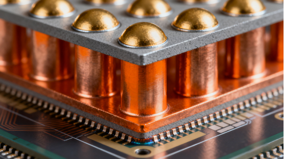
A copper pillar (Cu pillar) bump is a composite interconnect structure designed for high-density, high-performance semiconductor packages. It consists of three main components:
Copper Pillar: The central column provides both electrical conductivity and thermal dissipation, supporting the mechanical load of the bump. Copper’s high conductivity ensures minimal signal loss and efficient heat transfer.
Nickel Barrier Layer: Positioned between the copper pillar and the solder cap, the nickel layer serves as a diffusion barrier, preventing the formation of brittle intermetallic compounds (IMC) that can compromise reliability during high-temperature reflow.
Solder Cap: The top solder layer forms the final mechanical and electrical connection to the substrate or package during reflow. It enables a strong, stable bond while maintaining compatibility with standard assembly processes.
This layered structure allows Cu pillar bumps to achieve smaller pitch, higher I/O density, superior thermal performance, and longer lifespan compared with traditional solder bumps.
Step-by-Step Fabrication Process of Cu Pillar Bumps
The manufacturing of Cu pillar bumps is a precise, wafer-level process, typically including the following steps:
1. UBM Formation: Deposit the Under Bump Metallization (UBM) stack on the chip pads to provide adhesion, electrical contact, and diffusion protection.
2. Photoresist Application and Lithography: Apply photoresist and use photolithography to define the areas where copper pillars will be grown.
3. Electroplating the Copper Pillar: Plate copper onto the exposed UBM areas to form the pillar structure. Pillar height and diameter are carefully controlled to meet design specifications.
4. Electroplating Nickel Barrier Layer: Deposit a thin nickel layer on top of the copper pillar to serve as a diffusion barrier, enhancing long-term reliability.
5. Electroplating the Solder Cap: Plate a solder layer (often tin or tin–silver) onto the nickel to create the bonding surface for reflow assembly.
6. Photoresist Removal: Strip the photoresist to expose the finished Cu pillar bumps.
7. Reflow Formation: Heat the wafer to melt the solder cap, forming a spherical, reliable connection ready for subsequent packaging or substrate bonding.
This stepwise, wafer-level process allows Cu pillar bumps to achieve high uniformity, fine pitch capability (<50 µm), and excellent electrical and thermal performance, making them ideal for AI processors, GPUs, high-speed logic ICs, and automotive electronics.
Applications and Future Trends of Bumping Technology
Market Growth Trends in Advanced Packaging (Updated Data)
Bumping technology continues to drive the growth of advanced semiconductor packaging. According to Yole Développement data:
2.5D and 3D packaging is projected to grow at a 37% compound annual growth rate (CAGR), increasing from $4.3 billion in 2023 to over $28 billion by 2029. The growth is driven by high-performance computing, AI, networking, autonomous driving, personal computing, and gaming applications.
Fan-out (FO) packaging continues to expand, with telecom, mobile, and consumer electronics as major application segments.
Substrate-based packaging such as Flip Chip Ball Grid Array (FC-BGA) maintains steady growth, supporting mainstream high-performance ICs.
These trends highlight that bumping technology underpins the expansion of high-density, high-performance packages across multiple market segments, with 2.5D and 3D integration increasingly critical for enabling ultra-high bandwidth and dense I/O interconnects.
Key Application Areas
Bumping and Cu pillar technologies are essential in a variety of applications:
AI/HPC, GPUs, Data Centers: These devices require high I/O density and wide bandwidth, making Cu pillar bumps ideal for 2.5D/3D stacked architectures.
Smartphones & 5G SoCs: Cu pillar bumps are widely adopted to support high-speed signals and dense interconnects in compact form factors.
Automotive Electronics: Applications demand high-reliability bumps capable of withstanding extreme temperature and vibration conditions.
Image Sensors (CIS) & Power Management ICs (PMICs): Solder bumping, including ball placement methods, remains widely used for cost-effective, moderate-density interconnects.
These examples show how bumping technology is tailored to performance, density, and reliability requirements depending on the application.
Future Technology Directions
The evolution of bumping technology is closely tied to package miniaturization and performance enhancement:
Ultra-fine pitch (<20 µm): Enables higher I/O density for next-generation chips.
Micro-bumps and hybrid bonding: Support 3D integration and chip-to-chip interconnects, reducing electrical resistance and parasitics.
Thinner packages and 3D stacked structures: Facilitate compact device footprints while maintaining high functionality.
High-thermal-conductivity materials: Improve heat dissipation in high-power and high-speed applications.
In summary, bumping technology will continue to evolve toward finer pitches, denser integration, and higher thermal and electrical performance, enabling the next generation of AI, mobile, and automotive devices.

Conclusion
Bumping is a key semiconductor interconnect technology that forms tiny metal contacts between a chip and its substrate, enabling high-density connections for Flip Chip, fan-out, 2.5D/3D, and SiP packages. It shortens interconnect paths, reduces parasitic effects, and improves signal integrity, supporting higher I/O counts and bandwidth.
Solder bumps are cost-effective and mature, suitable for low- to mid-speed devices, while Cu pillar bumps offer higher reliability, better thermal performance, and finer pitch, making them ideal for high-speed and high-density applications. Solder bumps can be made by stencil printing, electroplating, or ball drop, each with trade-offs in cost, precision, and scalability.
The advanced packaging market is growing rapidly, with 2.5D and 3D solutions projected to reach over $28 B by 2029. Applications include AI/HPC, GPUs, 5G SoCs, automotive electronics, and sensors. Emerging trends include ultra-fine pitch, micro-bumps, hybrid bonding, and 3D integration. PCBMASTER supports this evolution by providing high-performance PCBs and interconnect solutions for cutting-edge packages.
In short, bumping is a crucial enabler of modern electronics, driving performance, density, and reliability in next-generation devices.
FAQs
What is the difference between Bumping and Hybrid Bonding?
Bumping creates discrete metal contacts—solder or Cu pillars—between a chip and substrate, relying on physical interconnects for electrical and mechanical connection. Hybrid bonding, on the other hand, combines direct metal-to-metal bonding and dielectric bonding at the wafer or chip level, enabling ultra-fine pitch (<10 µm), higher I/O density, and lower parasitic resistance. Essentially, bumping is a traditional point-to-point interconnect, while hybrid bonding allows more seamless, dense chip-to-chip integration.
When should Cu pillar bumps be chosen over solder bumps?
Cu pillar bumps are preferred when high I/O density, fine pitch, high reliability, or better thermal management are required. They are ideal for AI processors, GPUs, high-speed SoCs, and automotive electronics. Solder bumps are sufficient for low- to mid-speed devices or cost-sensitive applications, where ultra-fine pitch or extreme reliability is not critical.
Why can’t the UBM layer be omitted, and what failures may occur?
UBM (Under Bump Metallization) is essential because it provides adhesion, electrical contact, and diffusion protection between the chip pad and the bump. Without UBM, bumps may detach, experience metal diffusion, develop intermetallic brittleness, or fail under thermal stress. Skipping UBM would severely compromise both mechanical integrity and long-term reliability.
What are the main technical challenges with small-pitch bumps (e.g., 20 µm)?
At ultra-fine pitches, several issues arise:
Precise lithography and mask alignment are required to define bump locations.
Electroplating control must be extremely accurate to ensure uniform bump height and diameter.
Solder volume management is critical, as small deviations can cause bridging, voids, or misalignment.
These challenges make manufacturing more complex and demand advanced process control.
What is the role of bumping in Flip Chip versus Fan-out packaging?
In Flip Chip (FC), bumps directly connect the die to a substrate, providing short electrical paths for high-speed signals and high I/O density. In Fan-out (FO) packaging, bumps are part of a re-distribution layer (RDL) that extends I/O connections beyond the die footprint, allowing more interconnects in a thin, compact package. In both cases, bumping is essential, but in FO, it also enables package-level routing and increased integration beyond the chip itself.