


How Quick-Turn High-Precision PCB Prototypes Speed Up Product Development
In the race to bring innovative products to life, every hour counts. Quick-turn PCB prototypes make it possible to test ideas, refine designs, and solve problems almost as fast as they arise. For teams striving to stay ahead, they transform uncertainty into confidence and speed into a real advantage.
Introduction to Quick-Turn PCB Prototypes
Definition and Purpose
Quick-turn PCB prototypes are printed circuit boards designed and manufactured with speed as a top priority. Unlike traditional prototyping, which can take weeks, quick-turn PCBs are produced within days—or even hours—without sacrificing accuracy or reliability. Their purpose is to allow engineers and designers to test, validate, and refine circuit designs rapidly.
The key goals of quick-turn PCB prototyping are speed and efficiency. By shortening the production timeline, teams can move from concept to testing in a fraction of the time it would normally take. This approach reduces delays, accelerates design iterations, and enables faster decision-making during the development process.
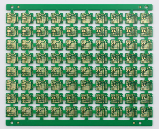
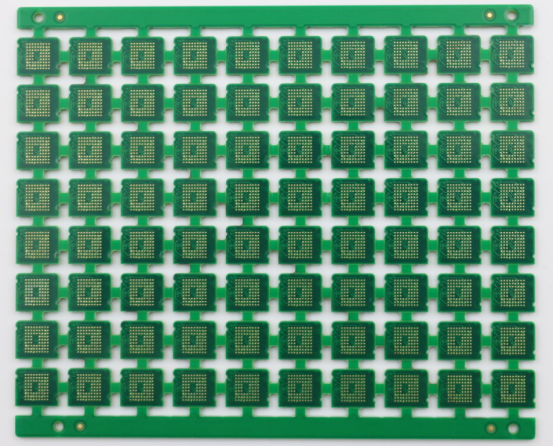
Several industries rely heavily on quick-turn PCB prototypes. Electronics manufacturers benefit from rapid testing of new consumer devices. Medical device companies use them to ensure compliance and safety while refining intricate circuits. Aerospace and defense projects leverage quick-turn PCBs to meet strict timelines without compromising high-precision requirements. In all these cases, the ability to produce a reliable prototype quickly is critical to innovation and competitiveness.
Importance in Modern Product Development
In today’s fast-paced market, product development cycles are shorter than ever. Rapid innovation requires prototyping methods that can keep up. Quick-turn PCBs allow companies to test ideas, evaluate functionality, and identify potential issues early in the design process.
One major advantage is the competitive edge gained through faster time-to-market. A prototype delivered in days rather than weeks can speed up validation, regulatory approval, and production planning. This means products reach customers sooner, giving companies a strategic advantage.
Early detection of design flaws is another critical benefit. By testing prototypes quickly, teams can identify and correct errors before moving to mass production. For example, a misrouted signal or insufficient trace width can be fixed immediately, avoiding costly revisions later. In essence, quick-turn PCB prototyping transforms uncertainty into actionable insights, helping teams make informed decisions while keeping schedules tight.
Key Benefits of Quick-Turn PCB Prototypes
Accelerated Development
Quick-turn PCB prototypes significantly shorten the design cycle, allowing engineers to explore concepts faster than traditional methods. Traditional prototyping can take weeks, often delaying testing and validation. In contrast, quick-turn PCBs can be produced in days or even hours, enabling teams to move from initial design to functional testing without long waits.
This accelerated development is especially valuable for projects with tight deadlines or fast-changing requirements. For example, a consumer electronics team can test a new device feature within a day, rather than waiting weeks for a conventional prototype. By reducing the gap between design and testing, teams can make informed decisions more quickly.
Faster Design Iterations
Quick-turn PCB prototyping allows multiple design versions to be tested and refined in rapid succession. Each iteration provides feedback that informs the next round of design improvements.
Step-by-step, the process typically works like this:
Initial Design: Engineers create the first PCB layout based on project requirements.
Prototype Fabrication: The PCB is manufactured using quick-turn methods.
Testing and Evaluation: The prototype undergoes electrical, functional, and environmental testing.
Refinement: Designers make adjustments based on test results, and a new prototype is produced quickly.
This cycle can repeat multiple times in a short period, accelerating optimization and ensuring the final design is robust and reliable.
Risk Mitigation
One of the key advantages of quick-turn PCBs is the early identification of design flaws. Detecting issues during the prototype stage prevents costly mistakes during mass production.
For example, if a signal trace is incorrectly routed or a component footprint is incompatible, these errors can be corrected immediately. Avoiding late-stage rework reduces both time and cost, ensuring projects stay on schedule and within budget. Quick-turn prototyping effectively transforms potential risks into manageable, actionable insights.
Reduced Turnaround Time
Quick-turn PCB processes streamline production and assembly, leading to significantly faster completion of prototypes. While traditional PCB prototyping might take several weeks, quick-turn methods can deliver fully assembled prototypes in as little as 24 hours.
For instance, a project requiring urgent validation can follow this timeline:
Day 1: Submit design files and confirm specifications.
Day 2: PCB is fabricated, assembled, and undergoes initial testing.
Day 3: Prototype is delivered, ready for functional evaluation.
This rapid turnaround enables faster decision-making, accelerates the overall development cycle, and keeps projects moving ahead without delays.
The Quick-Turn PCB Prototyping Process
Design Review and Optimization
The first step in quick-turn PCB prototyping is a thorough design review. Engineers evaluate the submitted design files to ensure manufacturability, checking for issues such as trace widths, component spacing, and layer stackups. Early detection of potential problems reduces errors during production and prevents costly delays.
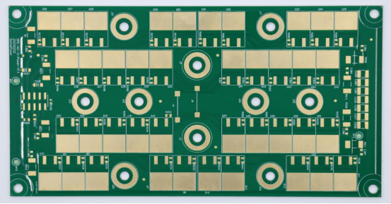
For complex PCBs, high-difficulty areas—like fine-pitch components, blind or buried vias, and high-speed signal routing—are identified during this stage. Addressing these challenges upfront ensures that even the most advanced designs can be fabricated quickly and reliably.
Material Sourcing and Preparation
After the design review, sourcing high-quality materials is essential for rapid prototyping. Quick-turn PCB manufacturers leverage established supply chains to acquire components and substrates quickly. This ensures that there are no bottlenecks in production, even for specialized or hard-to-find materials.
Material quality is closely monitored to prevent defects. By combining fast procurement with rigorous quality checks, manufacturers maintain reliability without slowing down the prototyping process. For example, components are tested for tolerances and PCB laminates are verified for thickness and dielectric properties before assembly begins.
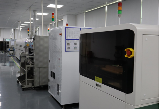
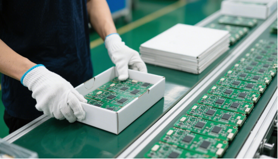
High-Precision Assembly and Testing
Once materials are ready, the prototype moves to assembly. Advanced techniques such as Surface Mount Technology (SMT) and automated pick-and-place systems enable precise component placement, even on high-density boards.
After assembly, automated inspection tools check solder joints, component alignment, and overall board quality. Functional testing ensures that the PCB performs as intended under real-world conditions. Each stage includes quality assurance checkpoints, minimizing the risk of errors and ensuring that the final prototype meets the design specifications.
Rapid Delivery and Feedback
Quick-turn PCB prototyping emphasizes speed without sacrificing collaboration. Once testing is complete, prototypes are delivered rapidly, often within 24–48 hours.
A collaborative feedback loop allows clients to review the prototype, provide input, and request adjustments. Any necessary modifications are incorporated into the next iteration, creating a continuous cycle of improvement. This approach ensures that prototypes evolve quickly and accurately, helping teams refine designs before moving to mass production.
Advantages of High-Precision Quick-Turn PCBs
Faster Design Changes
High-precision quick-turn PCBs allow engineers to respond immediately to testing results. If a component needs adjustment or a circuit trace requires rerouting, changes can be implemented quickly without waiting for lengthy production cycles.
This rapid adaptability supports continuous improvement of the design. Each iteration incorporates lessons learned from testing, enabling teams to refine performance, optimize layouts, and enhance reliability. Over time, this leads to a highly polished, fully functional PCB before moving to full-scale manufacturing.
Quicker Product Launch
Shortened development cycles directly accelerate product launch timelines. By reducing the time between design and testing, high-precision quick-turn PCBs help companies bring products to market faster, maintaining a competitive edge.
For example, a consumer electronics startup using quick-turn prototyping was able to reduce its time-to-market from eight weeks to just three weeks, enabling the product to launch ahead of competitors. Faster development cycles allow teams to meet market demands and capitalize on emerging opportunities without delay.
Early Problem Detection
Quick-turn PCB prototyping enables early detection and resolution of design issues before mass production begins. Errors such as signal interference, incorrect component placement, or insufficient trace widths can be identified and corrected immediately.
Compared with traditional prototyping, which may only reveal problems weeks later, quick-turn methods drastically reduce the risk of costly rework and project delays. Early problem detection protects project budgets, preserves timelines, and improves overall product quality.
Cost-Effective Small-Batch Production
High-precision quick-turn PCBs make small-batch production affordable and efficient. Since the prototyping process is optimized for speed and precision, manufacturing a limited quantity of boards incurs minimal additional cost.
This is particularly ideal for testing, validation, and pilot production phases. Engineers can produce multiple iterations in small quantities, evaluate performance, and make adjustments without committing to expensive full-scale runs. This approach balances quality, speed, and cost-effectiveness, especially for complex or high-value projects.
Overcoming Challenges in Quick-Turn Prototyping
Maintaining Quality Under Pressure
One of the main challenges in quick-turn PCB prototyping is maintaining high quality while working under tight deadlines. Advanced QA (Quality Assurance) processes ensure precision and reliability at every stage of production.
For complex boards with multiple layers, fine-pitch components, or high-speed circuits, rigorous testing protocols are essential. This can include automated optical inspection (AOI) to check solder joints, X-ray inspection for hidden defects, and functional testing to verify electrical performance. By implementing these checks systematically, manufacturers can deliver high-precision PCBs without compromising quality, even when turnaround times are extremely short.
Balancing Cost and Speed
Quick-turn prototyping requires a careful balance between speed and cost-efficiency. Optimizing production processes allows manufacturers to reduce lead times without significantly increasing expenses.
A step-by-step approach to cost-effective rapid production might include:
1. Design Optimization: Identify potential manufacturing challenges early to prevent costly delays.
2. Efficient Material Sourcing: Use established supply chains to secure components quickly while maintaining quality.
3. Streamlined Assembly: Implement automated processes like SMT placement and soldering to reduce manual labor.
4. Integrated Testing: Combine inspection and functional testing to catch defects early and avoid rework.
5. Iterative Feedback: Quickly incorporate client feedback to minimize additional production cycles.
By following this workflow, companies can produce high-quality prototypes quickly while keeping costs manageable, making quick-turn PCB prototyping a practical solution for both small and large-scale projects.
Choosing the Right Quick-Turn PCB Partner
Expertise in High-Complexity PCBs
A reliable quick-turn PCB partner must have extensive experience with high-complexity designs. This includes multi-layer boards, fine-pitch components, high-speed circuits, and advanced materials. Partners with this expertise can handle challenging layouts, ensuring manufacturability and consistent performance even for the most intricate designs.
Rapid Turnaround Times
Speed is critical in quick-turn prototyping. The right partner can deliver prototypes within 24 hours, allowing teams to test and iterate without delay. Real-world examples include companies receiving fully assembled multi-layer PCBs overnight to meet urgent product deadlines. Fast delivery keeps development cycles short and helps maintain a competitive advantage in fast-moving industries.
Competitive Pricing
Cost efficiency is another important consideration. High-quality quick-turn PCB services should offer small-batch production at competitive rates. This enables startups, R&D teams, and pilot projects to validate designs without incurring the high expenses of large-scale manufacturing.
Exceptional Customer Support
Effective collaboration is essential for smooth prototyping. A strong partner provides continuous communication and a feedback loop throughout the design, fabrication, and testing stages. This ensures prototypes meet specifications, allows quick adjustments, and creates a more efficient development process overall.
Recommendation: PCBMASTER
For companies seeking high-precision, rapid, and cost-effective quick-turn PCBs, PCBMASTER stands out as a trusted partner. With expertise in complex designs, the ability to deliver prototypes quickly, competitive pricing for small-batch runs, and exceptional customer support, PCBMASTER provides a comprehensive solution for all rapid prototyping needs. Choosing the right partner like PCBMASTER ensures that your PCB projects stay on schedule, on budget, and meet the highest quality standards.
Conclusion
Quick-turn PCB prototypes offer a strategic advantage for modern product development. By enabling faster design iterations, early problem detection, and rapid delivery, they help teams accelerate development while minimizing risk. Compared with traditional prototyping, quick-turn methods reduce delays, lower costs, and support continuous improvement, giving companies a clear competitive edge.
For businesses aiming to innovate efficiently and bring products to market faster, partnering with a high-precision PCB manufacturer is essential. With expert support, advanced capabilities, and rapid turnaround, the right partner ensures your prototypes are accurate, reliable, and ready for the next stage of production.
FAQs
What industries benefit the most from quick-turn PCB prototyping?
Quick-turn PCB prototyping is especially valuable in industries where innovation cycles are fast and precision is critical. Key sectors include:
Electronics: Consumer devices and gadgets that require rapid testing and iteration.
Medical devices: Circuits for diagnostic equipment, wearable devices, and safety-critical applications.
Aerospace and defense: High-complexity boards where reliability and strict timelines are essential.
These industries rely on quick-turn PCBs to reduce delays, improve product quality, and maintain competitiveness.
How do quick-turn PCBs reduce time-to-market?
Quick-turn PCBs accelerate the development process by enabling rapid testing, iterative design changes, and early problem detection. Shorter fabrication and assembly times allow engineers to validate designs in days instead of weeks. This speed ensures products can be launched faster, giving companies a competitive advantage and helping them respond quickly to market demands.
What is the difference between traditional PCB prototyping and quick-turn prototypes?
Traditional PCB prototyping: Often takes several weeks, with longer fabrication, assembly, and testing cycles. Design issues may only be detected late, leading to costly rework.
Quick-turn PCB prototyping: Focuses on rapid turnaround—sometimes within 24–48 hours—while maintaining high precision. Multiple design iterations can be tested quickly, and errors are identified early, reducing delays and costs.
Can small-batch PCB production be cost-effective with quick-turn methods?
Yes. Quick-turn prototyping optimizes processes to make small-batch production affordable. Engineers can produce multiple prototype versions in limited quantities for testing, validation, or pilot runs without incurring the high costs associated with full-scale manufacturing. This approach is ideal for R&D teams, startups, or projects with specialized components.
How do manufacturers maintain high quality under rapid prototyping timelines?
Manufacturers use rigorous quality assurance (QA) protocols at every stage of production, even under tight deadlines. Techniques include automated optical inspection (AOI), X-ray inspection for hidden defects, functional testing, and continuous monitoring of materials and assembly processes. These measures ensure that prototypes are precise, reliable, and perform as intended, despite the accelerated timeline.

