


PCB Plated Via Plugging A Small Process with Big Impact – A Key Technology for Enhancing PCB Reliability
Introduction
In high-end electronic devices, a circuit board the size of a fingernail might contain thousands of tiny holes. How these holes are processed directly determines the board’s performance and reliability. The manufacturing process for vias, including advanced plugging techniques, is critical for ensuring PCB reliability.
During PCB manufacturing, vias play the critical role of connecting different circuit layers. However, if not handled correctly, these very holes can become the “Achilles’ heel” of the board.
Plated Via Plugging is the key process that addresses this issue. This article delves into this seemingly minor but crucial PCB technology.
From Stairs to Bridges: Understanding PCB Vias
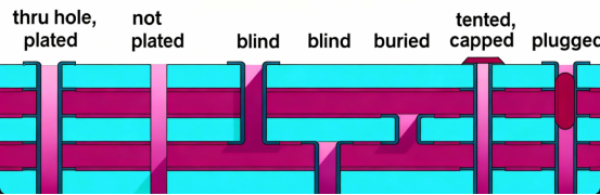
To appreciate the value of plated via plugging, we must first understand vias. Imagine a multi-story building: vias are like the staircases connecting different floors, allowing people to move between them freely.
In a PCB, a via is a small hole, typically drilled as a through hole, used to connect copper traces on different circuit layers. This connection is achieved by plating the hole walls, as well as the annular ring, with a conductive material, typically copper, to ensure electrical connectivity. Vias enable connections between the outer and inner layers, as well as to other layers of the PCB.
As electronic devices trend towards being “lighter, thinner, shorter, and smaller,” component density on PCBs has increased. With the widespread use of SMT (Surface Mount Technology) and BGA (Ball Grid Array) packages, the requirements for via processing have become more demanding.
Why Do We Need to "Plug" Vias?
In PCBA manufacturing, “via plugging” is a term often mentioned but not always fully understood by clients. In PCB assembly processes, proper via fill techniques are essential for ensuring reliable interconnections and high-quality assembly. Simply put, via fill involves filling or covering the via with solder mask ink, resin material, or metallic material to fill vias and create a filled via. Manufacturers may fill vias using resin material or solder resist, and the curing process is critical for achieving a flat surface. Solder mask covers, via tenting, and vias tented are alternative methods for protecting vias, each with their own advantages. Liquid photo imageable solder mask is commonly used for via plugging and tenting, and the surface tension of the solder resist ink affects the quality of the fill. But why go through the trouble of plugging these holes?
1. Preventing Solder Shorts
During wave soldering or reflow soldering, molten solder can easily “wick” through unplugged vias to component pins or under BGA pads, causing solder shorts. To prevent this, solder mask covers or solder resist are applied to vias, creating a protective barrier that stops solder from entering the holes during assembly.
This is particularly problematic when vias are placed near BGA pads, as solder can travel through the hole to the top side, leading to serious short circuits.
2. Avoiding Contaminant Entrapment
If vias are left unplugged, flux or post-solder residue can become trapped inside. However, using resin material to fill the vias and applying a controlled curing process helps prevent contamination and ensures a reliable seal. This can lead to white corrosion or solder ball formation, adversely affecting electrical performance and reliability. Residual flux in humid environments can accelerate copper trace corrosion, potentially causing open circuits or leakage.
3. Enhancing Signal Integrity
In high-frequency or high-speed digital circuits, hollow vias cause impedance discontinuities, leading to signal reflection and crosstalk.
Via tenting and vias tented are alternative methods used to cover vias and improve signal integrity in certain PCB designs.
For high-speed boards with strict signal requirements (e.g., USB 3.0/PCIe interface boards), conductive via filling significantly reduces signal return loss, ensuring stable transmission.
4. Improving Heat Dissipation and Current Capacity
For power components or high-current traces, vias filled with conductive material—especially those with the metallic nature of copper conductive fills—act like “micro heat pipes,” efficiently transferring heat or current to the other side, thereby improving thermal management and current-carrying capacity.
The choice between conductive or non-conductive via fill materials can significantly affect thermal expansion and long-term reliability, as differences in material properties may lead to mechanical stresses or fractures under high heat or current.
5. Increasing Mechanical Strength, Solder Mask Coverage, and Surface Planarity
If vias remain hollow, processes like Hot Air Leveling (HAL) or hot air reflow can cause outgassing, potentially leading to voids or cracks in the cured ink. Solid plugging results in a flatter board surface and reduces issues like solder bridging and solder balls, as a flat surface is achieved through a controlled curing process and the creation of a filled hole.
Design Considerations for Via Plugging
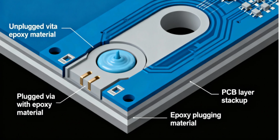
When designing a printed circuit board (PCB) that requires via plugging, careful planning is essential to achieve both reliability and optimal performance. The choice between using a non conductive material or a conductive material for via plugging depends largely on the board’s intended function. For example, in via in pad designs—common in high-density assemblies—non conductive epoxy fill is often selected to prevent solder wicking and ensure a perfectly flat, solderable surface for component mounting. This approach is especially important for BGA and fine-pitch components, where even minor solder leakage can compromise the electrical connection.
On the other hand, conductive filled vias are preferred in applications where higher thermal conductivity is needed, such as in power electronics or boards with components that generate significant heat. These filled vias help to efficiently transfer heat away from sensitive areas, improving the overall thermal management of the circuit board.
Designers must also consider the hole size, shape, and placement of each via. Smaller via holes are more challenging to fill completely, increasing the risk of voids or incomplete plugging, which can lead to solder leakage or weak electrical connections. The type of solder mask used—such as LPI solder mask—also plays a crucial role in covering the via and preventing solder from flowing into the hole during assembly. By carefully selecting the appropriate via plugging method, fill material, and solder mask, designers can prevent solder wicking, enhance the reliability of the electrical connection, and ensure the long-term performance of the printed circuit board.
Fill Material Options for Plated Via Plugging
Selecting the right fill material for plated via plugging is a critical step in ensuring the durability and functionality of printed circuit boards. Non conductive epoxy resin is widely used for via plugging because it provides excellent structural support and effectively prevents solder wicking during the assembly process. This type of fill material is especially suitable for applications where electrical isolation is required, such as in non conductive via plugging or via in pad designs.
For applications demanding higher thermal conductivity, conductive materials like copper or silver epoxy are often chosen. These materials allow filled vias to naturally wick heat away from components, which is vital for high-power or high-frequency circuit boards. Conductive filled vias not only improve heat dissipation but also help maintain a strong electrical connection across different layers of the PCB.
The choice of fill material should also take into account its compatibility with the surrounding laminate and copper features, as well as its ability to withstand the thermal and mechanical stresses of the assembly process. Using a fill material with low thermal conductivity may result in a weak electrical signal or inadequate heat management, while a well-chosen fill can enhance both the structural support and electrical performance of the board. Ultimately, the fill material—whether non conductive epoxy, silver epoxy, or another option—should be selected based on the specific via plugging or via filling method, the assembly requirements, and the desired reliability of the finished circuit board.
Various Plated Via Plugging Process Methods
In PCB fabrication, several plated via plugging process methods are available, each tailored to different design and assembly needs. The via filling process involves injecting a fill material—such as epoxy resin or a conductive material—into the via hole to provide robust structural support and prevent solder wicking during soldering. This method is particularly effective for applications where a solid plug is needed to support surface mount components or to enhance the board’s mechanical strength.
Alternatively, the via plugging process uses a non conductive material, such as solder mask, to seal the via hole. This approach is commonly used to prevent solder from entering the via during the assembly process, especially in high-density designs where vias are located close to component pads. The choice between via filling and via plugging depends on factors such as the type of components used, the assembly process, and the required level of reliability.
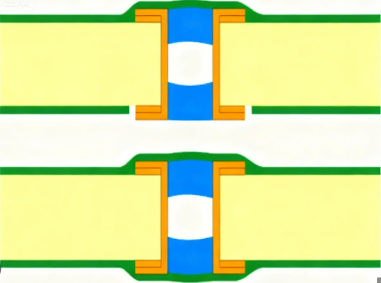
For designs that require a perfectly flat, solderable surface—such as via in pad configurations—the via hole may be plugged with a non conductive material and then plated over with copper, a process sometimes referred to as vias plated shut. This creates a smooth, continuous copper surface that is ideal for mounting BGAs and other fine-pitch components. Each of these process methods plays a vital role in preventing solder wicking, providing structural support, and ensuring the long-term reliability of the printed circuit board.
Various Plated Via Plugging and Via Filling Process Methods
Several technical approaches exist for plated via plugging, each with its own applications and characteristics. Via fill techniques are used to fill vias and create a filled via, ensuring reliable connections between the copper pad and the inner layers or other layers of the PCB.
During the manufacturing process, the hole barrel is plated using processes such as electroless copper deposition to ensure the entire surface is conductive and provides robust electrical connectivity. This step is critical for achieving a reliable filled via.
In high-density PCB designs, via-in-pad technology allows vias to be placed directly under a component pad, bga pad, or active pad, which is often preferred over traditional dog bone patterns for improved routing and space efficiency.
Liquid photo imageable solder mask is commonly used for via plugging, and the surface tension of the ink plays a significant role in the quality of the fill, affecting the completeness and reliability of the via fill.
Proper via fill and plugging techniques are essential for reliable PCB assembly and optimal solder paste application, ensuring strong solder joints and preventing defects.
An experienced engineering team is crucial for selecting the right process and materials to achieve high-quality, reliable results in advanced PCB manufacturing.
Conductive vs. Non-Conductive Plugging
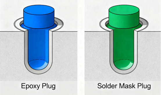
Based on the filling material, plugging processes fall into two main categories:
·Non-Conductive Plugging: Typically uses epoxy resin or LPI (Liquid Photoimageable) Ink to fill the via. In this case, a resin material is used as a non-conductive fill to prevent contamination, provide mechanical support, and ensure electrical insulation. After filling and leveling, the outer layers retain the copper plating to maintain conductivity. This is the most common method; even with non-conductive fill material, the via continues to conduct electricity normally.
·Conductive Plugging: Suitable for boards requiring high thermal conductivity or high current carry capacity, such as those with power devices or IC heat dissipation areas. Common materials include metallic fillers, with copper conductive fills being a primary example. The choice between conductive or non-conductive materials depends on the application requirements. Thermal conductivity typically ranges between 3.5–15 W/mK, lower than pure copper but superior to resin.
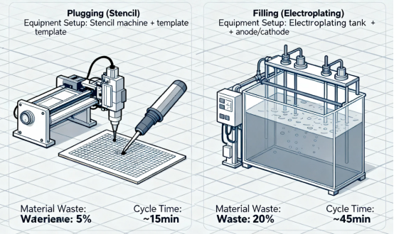
Pre-HAL vs. Post-HAL Plugging Processes
Plugging can also be categorized based on its sequence relative to the Hot Air Leveling process:
·Post-HAL Plugging Process: The sequence is “Solder Mask Application → HAL → Plugging → Curing”. In this workflow, the curing process is a critical step to ensure the integrity and reliability of the solder mask covers over the vias. Proper curing helps prevent defects such as dimples and maintains surface flatness, although issues like ink smearing on the board surface and an uneven finish can still occur.
·Pre-HAL Plugging Process: This includes various methods, such as plugging with aluminum foil, curing, then pattern transfer after polishing; or directly applying solder mask after aluminum foil plugging. In each case, the curing process is essential for achieving robust solder mask covers, ensuring a flat plugging surface, and preventing quality issues like blistering or material detachment around the via during HAL.
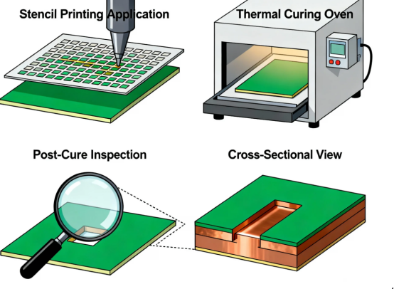
Quality Inspection for Plugging Processes1
Ensuring the quality of via plugging is essential for the reliability and performance of printed circuit boards. The inspection process begins with a thorough visual examination of the via holes to detect any obvious defects, such as air bubbles, incomplete fills, or signs of solder leakage. These issues can compromise the electrical connection and lead to failures during the assembly process or in the field.
Electrical testing is also a key part of the inspection process, verifying that each via maintains a solid electrical connection between layers. Advanced inspection techniques, such as X-ray imaging, are increasingly used to detect hidden defects within the via plugging, such as voids or irregularities that are not visible from the surface. These methods help ensure that the fill material is properly distributed and that the via plugging process has been executed correctly.
In addition to inspecting the via holes themselves, it is important to check the condition of the solder mask covering the plugged vias. Defects such as cracks, delamination, or poor adhesion can lead to solder leakage or environmental damage, ultimately affecting the reliability of the PCB. By combining visual, electrical, and advanced inspection methods, manufacturers can ensure that the via plugging process meets the highest standards for quality and reliability.
Quality Inspection for Plugging Processes2

The quality of the plugging process is paramount, and the industry employs several inspection methods. Inspection focuses on the quality of the filled hole, the flat surface of the board, and the integrity of the hole barrel plating.
1. Plated Copper Quality Check
An innovative method utilizes light transmission principles: Test holes are placed in non-product areas of the board substrate. Immediately after copper deposition, the quality is checked at these points.
Light is shone from the side with the copper layer towards the side without it, observing whether light passes through the copper layer on the side without the protective film. During this inspection, the entire surface of the via, including the copper conductive layer, is checked for uniformity and thickness to ensure reliable electrical performance.
Since resin is transparent or semi-transparent, while copper has very poor light transmission, a sufficiently thick copper layer on the resin surface should allow very little light through. If the copper layer is too thin or has cracks/voids, light transmission will be higher.
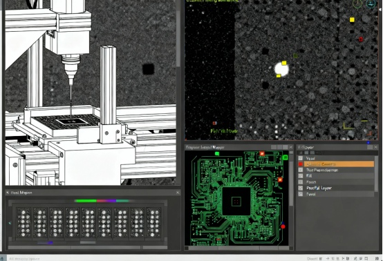
2. X-ray Non-Destructive Testing
Since the internal copper plating condition cannot be observed externally, defective samples were traditionally cross-sectioned (destroyed) to find flaws.
Now, 2D X-ray can be used for preliminary, non-destructive inspection of the overall copper plating and potential fractures. If more detailed observation of the entire hole wall plating is needed, 3D X-ray CT scanning can be employed. This method allows for detailed inspection of the hole walls and verifies connectivity to the inner layers.
3. Voiding Control
In HDI (High-Density Interconnect) PCB manufacturing, controlling the void ratio in copper-filled vias via X-ray is crucial. Voids in the via fill or resin material can compromise the reliability of the filled via by reducing electrical insulation, mechanical support, and increasing the risk of contamination.
According to IPC-A-610G standards, for Class 3 high-reliability electronic products, the void area in via fills should not exceed 25%. For Class 2 standard electronic products, a void rate of up to 40% might be acceptable.
Common Issues with Via Plugging
While via plugging offers significant benefits for PCB reliability, several common issues can arise if the process is not carefully controlled. One frequent problem is solder wicking, where solder flows into the via hole during the assembly process, potentially causing shorts or weak electrical connections. This can often be prevented by using a non conductive epoxy fill or by sealing the via with a high-quality solder mask.
Another issue is the formation of air bubbles within the fill material. Air bubbles can create voids that weaken the structural support of the via and disrupt the electrical connection between layers. To minimize this risk, it is important to use a fill material with the appropriate viscosity and to ensure that the via hole is thoroughly cleaned and prepared before filling.
Using a conductive material that is not compatible with the PCB’s laminate or copper features can also lead to problems, such as weak electrical connections or even short circuits. Careful selection of both the via plugging method and the fill material is essential to avoid these pitfalls. By addressing these common issues—through proper material selection, process control, and thorough inspection—manufacturers can ensure that via plugging enhances, rather than compromises, the performance and reliability of the printed circuit board.
Application Scenarios for Plugging Processes
Via plugging isn’t necessary for all PCBs but is particularly critical in the following scenarios:
PCB Assembly and High-Density Designs:
Proper via fill and filled via techniques are essential for reliable PCB assembly, especially in high-density designs. Via fill improves electrical reliability, mechanical strength, and thermal management. Filled vias and copper pad connections are often required to ensure robust interconnections between inner layers and other layers of the board.
BGA and Fine-Pitch Components:
When assembling BGAs and fine-pitch components, filled vias are often placed directly under a component pad, bga pad, or active pad. Via-in-pad designs are sometimes used instead of traditional dog bone patterns to save space and improve routing. These approaches help prevent solder wicking and ensure a flat surface for reliable solder joints.
High-Frequency and High-Speed PCBs:
A flat surface is required for reliable solder paste application and proper reflow. Liquid photo imageable solder mask is often used to cover or fill vias, providing planarity and environmental protection. Solder resist and solder mask covers are also applied to prevent contamination and improve reliability.
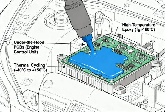
High-Power Electronic Equipment:
In high-power applications, the choice between conductive or non-conductive resin material for via fill affects thermal expansion and overall reliability. The right resin material can help manage mechanical stresses and prevent fractures due to differences in thermal expansion.
HDI and Microvia Designs:
For HDI and microvia designs, electroless copper deposition is sometimes used to ensure connectivity to inner layers and other layers. Conductive polymer filling can further enhance current flow and thermal management.
An experienced engineering team is essential for selecting the right materials and process steps, including managing surface tension during via fill, applying solder mask covers or solder resist, and ensuring high-quality, reliable PCB manufacturing.
BGA and Fine-Pitch Components
PCBs for SMT and BGA assembly, especially when filled vias are placed directly under a component pad, bga pad, or active pad, must undergo via plugging before final surface finish (like ENIG) to ensure soldering quality. This is absolutely essential when vias are placed directly on BGA pads, facilitating reliable BGA soldering. In high-density designs, via-in-pad or active pad approaches with filled via technology are often used instead of traditional dog bone patterns to save space and improve routing.
High-Frequency and High-Speed PCBs
In high-frequency and high-speed PCB design, unfilled vias cause impedance discontinuities, signal reflection, and EMI interference. Plugging the vias—especially using a liquid photo imageable solder mask to achieve a flat surface—is crucial for reliable signal transmission, as the surface tension of the ink directly affects the quality and completeness of the via fill. This approach helps mitigate these effects, improving signal integrity.
High-Power Electronic Equipment
For power components or high-current traces, vias filled with conductive material—whether using conductive or non-conductive resin material—require careful consideration of thermal expansion and the metallic nature of the fill, as these factors impact reliability, heat dissipation, and current-carrying capacity. Thermal vias for power or heat management often use thermally conductive plugging materials.
HDI and Microvia Designs
HDI and microvia technologies, such as via-in-pad and stacked microvias, require planarized structures, often achieved through processes like electroless copper deposition to ensure reliable connections to inner layers and other layers. Plugging is vital for achieving the necessary surface flatness.
Summary
Today, the rapid development of 5G, AI, and IoT is placing higher demands on PCBs. “Micro-processes” like plated via plugging are playing an increasingly important role. From smartphones to aerospace equipment, from medical electronics to autonomous driving, reliable plated via plugging is a cornerstone ensuring the long-term stable operation of electronic devices.
The next time you hold a slim smartphone or wear a smartwatch, consider the thousands of “filled holes” inside – it is these unseen, minute details that underpin the efficient operation of modern electronic devices.
FAQs
Q: What is PCB plated via plugging?
A: It's a PCB manufacturing process: First, the walls of the via are plated with a metal (usually copper) to enable electrical connectivity between layers. Then, the hole is filled with a material like resin and sealed.
Q: Why choose plated via plugging over non-plated plugging?
A: Plated vias ensure electrical conductivity between layers, while plugging prevents solder wicking, short circuits, and signal interference. This is particularly critical for high-density and high-speed PCBs.
Q: What materials are commonly used for via plugging?
A: Epoxy resins are most common (available in conductive and non-conductive types). Some applications use solder mask ink, but resin offers better stability in high-frequency scenarios.
Q: What problems does it solve?
A: It prevents solder balls from falling into the via and causing shorts, reduces signal reflection caused by via stubs, and blocks dust or liquids from entering the hole, thereby extending PCB lifespan.
Q: What are the key quality inspection points for plated via plugging?
A: Ensuring the filled vias are free of voids or air bubbles, verifying strong adhesion between the resin and plated copper, and checking for a flat surface after curing (no protrusions that could affect component mounting).
Q: Is plated via plugging suitable for all PCBs?
A: It's primarily used in high-density PCBs where signal integrity and reliability are critical (e.g., 5G equipment, servers). Simple, low-layer PCBs generally don’t require it.
Q: Does plated via plugging increase PCB cost?
A: Yes – the additional plating and plugging steps do increase cost. However, for high-performance products, it offers strong cost-effectiveness by preventing potential failures associated with non-plated or unplugged vias.
Author: Jack Wang

